
While Nikola Tesla is justifiably praised for many contributions to electrical engineering, his battle with Thomas Edison over alternating vs. direct current is entering a new stage decades after both were laid to rest.
Researchers, engineers and industrialists from across the world met recently in Leuven, Belgium as part of the 2017 Imec Technology Forum (ITF). The experts dove into many far-reaching topics, but one centered on a century-old debate: DC vs. AC grids.
As it turns out, there are new wrinkles, and DC ‘Nanogrids’ may shape our electrical future.
Today’s electricity infrastructure typically transports alternating current (AC), which in turn means most homes and businesses are AC wired. But as ITF speakers like Professor Johan Driesen (KU Leuven and EnergyVille) pointed out, up to two-thirds of electrical devices use DC. AC flows from sockets, but converters transform it into the DC voltage that entertains, conditions air, cleans clothes, cooks food and lights the night.
So why are grids transmitting AC when DC is what most appliances, tools and toys really need? It’s about distance and the battle between Thomas Edison and his ‘upstart’ engineer, Nikola Tesla.
Late in the 19th century when electrification was a new idea, two schools of thought battled for preeminence. Edison had his backers and bankers, as did Tesla. The decision ultimately turned on the fact that by using transformers, alternating current proved more practical since building DC electrical grids would have involved keeping generation much closer to loads, requiring more power plant infrastructure—a costly gamble in the minds of many. AC won that argument, but the choice created massive centralized power plants churning out juice by burning fossil fuels.
What about today? We now know that burning fuels at industrial scale leads to CO2, other greenhouse gases and carcinogens belching out smokestacks. Over the decades all that burning to generate power has led to global warming and the climate change corundum we face today.
Experts point to potential savings of wiring new homes and businesses for DC: up to 35 percent in capital expenses, plus a 10 percent reduction in electricity consumption. But no one should be deceived into thinking this will be easy. It is also difficult to calculate how long it would take for this change to have real impact. In this edition we explore the benefits of the DC Nanogrid concept through an imec article that makes its case. Get the facts, and then you can decide: Will the future favor Edison’s DC view, or will we hold to Tesla’s AC vision?

Infineon Technologies AG expands its 1200 V discrete IGBT product portfolio by offering up to 75 A. The devices are co-packed with a full rated diode in a TO-247PLUS package. The new TO-247PLUS 3pin and 4pin packages serve the growing demand for higher power density and highest efficiency in discrete packages. Typical applications with a blocking voltage of 1200 V requiring high power density are drives, photovoltaic, and uninterruptible power supplies (UPS). Additional applications comprise battery charging and energy storage systems.
Compared to a regular TO-247-3 package, the new TO-247PLUS package can provide double current rating. Due to the removal of the screw hole from the standard TO-247 package, the PLUS package has a larger lead frame area and thus can accommodate bigger IGBT chips. Now, up to 75 A 1200 V co-packed IGBTs with the same small footprint are available for the first time. The larger lead frame provides a lower thermal resistance of the TO-247PLUS package, leading to an improved heat dissipation capability.
For designers looking to improve the switching losses, the TO-247PLUS 4pin package features an extra Kelvin emitter source pin. This allows for an ultra-low inductance gate-emitter control loop and reduces the total switching losses E (ts) by more than 20 percent. The 1200 V IGBTs in TO-247PLUS 3pin and 4 pin packages can be used to increase the system power density. Additionally, they can reduce the number of power devices used in parallel, increase system efficiency or improve system thermal conditions.
Navitas announces GaN power reference design
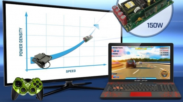
Navitas Semiconductor has launched an 150W AC-DC reference design using the company’s GaN power ICs. At over 21 W/in3 and at over 95 percent efficiency, the NVE021A is said to be more than two times smaller than typical commercial designs and 40 percent smaller than previous best-in-class today.
The design can be adapted over a power range of 85-500W to enable a new class of converters to address ultra-thin LED TVs, fast-charging laptop adapters, high-density gaming systems, all-in-one PCs and any other systems seeking high-density or high efficiency power solutions.
Navitas GaN Power ICs enable high-frequency switching to shrink passive components. Soft-switching critical-conduction mode (CrCM) PFC and LLC DC-DC stages operate at working frequencies up to 300 kHz (600 kHz during start-up, burst mode) - the fastest-possible speed provided by off-the-shelf controller ICs available today.
The NVE021A reference design (150W, AC to 12V DC) is available direct from Navitas at a price of $465 each, which includes a user guide / test report with all schematic and layout design files, plus bill of material.
“Navitas GaN Power ICs enable breakthrough adapter performance in small size and high efficiency with simple, practical and economical designs”, explained Stephen Oliver, the company’s VP of Sales & Marketing.
“Silicon-based designs are slow, bulky and heavy. This reference design is the first in a series that will demonstrate how new GaN power ICs can increase frequencies five times or more with efficiencies of 95 percent, enabling a three to five times increase in power densities for a broad range of AC-DC applications”.

ABB is bringing affordable, safe and reliable electricity to remote communities thanks to its new integrated microgrid solution, MGS100, that enables solar power and battery energy storage.
The MGS100 has been built to perform in extreme environments, and can transform lives and businesses for the better in places that struggle to access affordable and reliable electricity.
The scalable system can be connected to multiple power sources to provide electricity for remote places that are not connected to the main grid, or reliable back-up power for small commercial and industrial facilities using an inconsistent grid supply, enabling social and economic development.
MGS100 brings together all the components required for a sustainable microgrid in a single device, making it extremely versatile and flexible. It can tap into cost efficient, renewable energies such as solar photovoltaic [PV] and batteries.
By prioritizing abundant local solar power during the day, the MGS100 switches to battery mode after dark and only uses an AC generator for the rest of the night if the battery runs out. Any excess energy produced throughout the day is used to charge the batteries.
Seamless transition between the grid and the microgrid allow operations to continue while the grid is down, and battery energy storage minimizes the need to purchase electricity from local utilities.
Encased in a single container, the MGS100 has three power ratings – 20kW, 40kW, 60kW nominal load power. Installation is quick and easy, as it is factory tested and embedded DC and AC protections make it ready to connect. With the added benefit of remote monitoring, vital diagnostics are always available and maintenance is simple.
The modular scalable design means that capacity can be increased as and when required, and it can even be connected to the grid if this becomes available.
ABB’s President of Electrification Products, Tarak Mehta, said: “At ABB we are committed to using the latest technical advancements to support everyone in society and create a new world of opportunity for these often remote and hard to reach communities. The MGS100 is the first microgrid solution of its kind that makes access to affordable and reliable power a reality, creating life changing opportunities, improving basic living standards and unlocking economic development.”
The MGS100 will be widely available at the end of 2017. ABB is currently seeking partners to trial the microgrid solution. For further information about the product and trial opportunities contact Erika Velazquez, Global Product Marketing Manager Microgrid.
EPC launches 30V GaN half bridge
EPC has announced the EPC2111, 30 V enhancement-mode monolithic GaN transistor half bridge. By integrating two eGaN power FETs into a single device, interconnect inductances and the interstitial space needed on the PCB are eliminated, according to the company.
This increases both efficiency (especially at higher frequencies) and power density, while reducing assembly costs to the end user's power conversion system.
The EPC2111 is suitable for high frequency 12 V to point-of-load DC-DC conversion. Each device within the EPC2111 half-bridge component has a voltage rating of 30 V. The upper FET has a typical RDS(on) of 14 mΩ, and the lower FET has a typical RDS(on) of 6 mΩ.
The EPC2111 comes in a chipscale package for improved switching speed and thermal performance, and is 3.5 mm x 1.5 mm for increased power density.
A primary application is notebook and tablet computing because their power conversion circuitry typically occupies nearly half of the space and defines the height of the motherboard. The high frequency capability of GaN reduces the size required for power conversion and thus will drive significant size reductions of next generation mobile computing, says EPC.

StratEdge Packages to Include High-Power GaN Transistors and MMICs
StratEdge Corporation, a company that makes high performance semiconductor packages for microwave, millimeter-wave, and high speed digital devices, has expanded its LL family of high-power laminate copper-moly-copper (CMC) base packages to include both GaN transistor and MMIC device packages and package assembly services.
The packages can now accommodate large MMICs, with die attach areas as high as 5.92 x 12.14mm. They operate at frequencies from DC to as high as 63GHz for applications in communications, radar, automotive, aerospace, defense, and those requiring high power millimeter-wave signals.
In addition to the packages, which are manufactured in StratEdge’s San Diego, California facility, StratEdge offers complete automated assembly and test services for these packages, including gold-tin solder die attach.
These assembly processes are said to routinely generate >96 percent void-free attachment with bond line thicknesses of <6 microns when used with the new LL series of packages. This is particularly important for GaN power amplifiers where efficient thermal transfer is critical for improved operation and reliability of the device.
The LL family of CMC-base packages dissipate heat from high-power compound semiconductor devices, such as GaN, GaAs, and SiC. These laminate power packages are built with a base material ratio of 1:3:1 CMC, which provides a good thermal match for alumina-based materials and a GaN chip.
"StratEdge was one of the first to market with laminate power packages for GaN devices," said Tim Going, StratEdge president. "StratEdge has continued to develop packages to handle the requirements of new materials and devices. Our LL family additions can handle frequencies up to 63 GHz and large MMIC devices, and our precision automated assembly and test services enable the chips to operate with the efficiency and electrical integrity they were designed to achieve.”

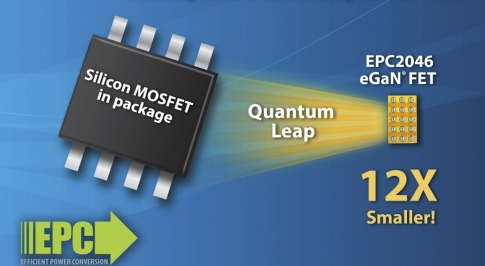
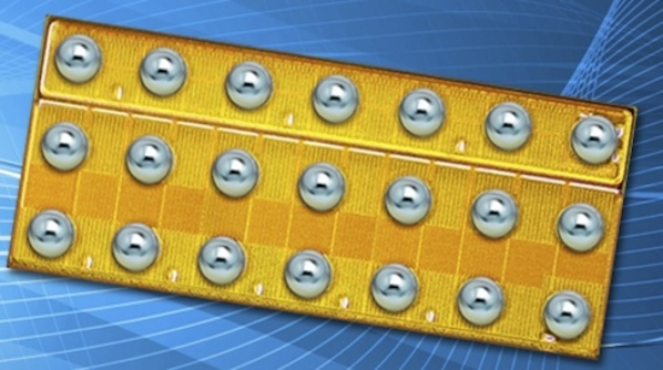
EPC Introduces 200V GaN Power Transistor
EPC has announced the EPC2046 power transistor for use in applications including wireless power, multi-level AC-DC power supplies, robotics, solar micro inverters, and low inductance motor drives.
The EPC2046 has a voltage rating of 200 V and maximum RDS(on) of 25 mΩ with a 55 A pulsed output current. The chip-scale packaging of the EPC2046 is said to handle thermal conditions far better than the plastic packaged MOSFETs since the heat is dissipated directly to the environment with chip-scale devices, whereas the heat from the MOSFET die is held within a plastic package. It measures 0.95 mm x 2.76 mm.
“Manufactured using our latest fifth-generation process, the EPC2046 demonstrates how EPC and GaN transistor technology is increasing the performance and reducing the cost of eGaN devices," said Alex Lidow, EPC’s co-founder and CEO.
“This opens up entirely new applications beyond the reach of the aging silicon MOSFET and offers a big incentive for users of MOSFETs in existing applications to switch. This latest product is further evidence that the performance and cost gap of eGaN technology with MOSFET technology continues to widen," he added.
The EPC9079 development board is a 200 V maximum device voltage, half bridge with onboard gate driver, featuring the EPC2046, onboard gate drive supply and bypass capacitors. This 2inch x 1.5inch board has been laid out for optimal switching performance and contains all critical components for easy evaluation of the EPC2046 eGaN FET.The EPC2046 eGaN FETs are priced for 1K units at $3.51 each.

To support its accelerating sales growth in Asia Pacific, Efficient Power Conversion Corporation (EPC) has announced that Roy Chang has joined the EPC as VP of sales for Greater China and Southeast Asia.
Chang joins EPC from Transphorm, where he was the VP of sales, Taiwan. Before joining EPC, Chang held R&D, technical sales, as well as sales and marketing leadership positions with Acer and Texas Instruments.
Chang has over 20 years of experience in R&D, technical sales, and marketing within the computer and semiconductor industry. His primary responsibilities at EPC are creating and implementing sales strategies to achieve the company’s sales objectives in Greater China and Southeast Asia. He is based in Taipei, Taiwan.
“As a customer-oriented engineer, Roy Chang has gained solid sales, customer and distribution management experience in multinational organizations including ramping new technology sales. He has a proven track record of managing sales, marketing, and FAE organization to increase values for customers and turn new business opportunities into results,” said Nick Cataldo, senior VP of Global sales and marketing, EPC.
“I look forward to Roy’s contribution to our sales growth; assisting me in expanding our customer base, maximizing new business acquisition, and capturing new markets throughout Asia Pacific,” commented Stephen Tsang, VP of sales, Asia Pacific, EPC.
“I am excited to have the opportunity to work with the team members at EPC. With my experience in ramping new technology sales, I look forward to contributing to EPC in creating design wins using our GaN FETs and integrated circuits to enhance our customers’ products,” said Chang.
Imec, a leading research and innovation hub in nano-electronics and digital technology, has announced that it has developed 200V and 650V normally-off/enhancement mode (e-mode) on 200mm/8-inch GaN-on-Silicon wafers, achieving a very low dynamic Ron dispersion (below 20 percent) and state-of-the-art performance and reproducibility. Stress tests have also shown a good device reliability. Imec’s technology is ready for prototyping, customized low-volume production as well as for technology transfer.
GaN technology offers faster switching power devices with higher breakdown voltage and lower on-resistance than silicon (Si), making it an ideal material for advanced power electronic components. Imec’s GaN-on-Si device technology is Au-free and compatible with the wafer handling and contamination requirements for processing in a Si fab. A key component of the GaN device structure is the buffer layer, which is required to accommodate the large difference in lattice parameters and thermal expansion coefficient between the AlGaN/GaN materials system and the Si substrate. Imec achieved a breakthrough development in the buffer design (patent pending), allowing to grow buffers qualified for 650 Volt on large diameter 200mm wafers. This, in combination with the choice of the Si substrate thickness and doping increased the GaN substrate yield on 200mm to competitive levels, enabling low-cost production of GaN power devices. Also, the cleaning and dielectric deposition conditions have been optimized, and the field plate design (a common technique for achieving performance improvement) has been extensively studied. As a result, the devices exhibit dynamic Ron dispersion below 20% up till 650 Volt over the full temperature range from 25°C to 150°C. This means that there is almost no change in the transistor on-state after switching from the off-state, a challenge typical for GaN technology.
“Having pioneered the development of GaN-on-Si power device technology on large diameter substrates (200mm/8-inch), imec now offers companies access to its normally-off/e-mode GaN power device technology through prototyping, low-volume manufacturing as well as via a full technology transfer” stated Stefaan Decoutere, program director for GaN technology at imec. “Next to enhancement mode power device switches, imec also provides lateral Schottky diodes for power switching applications. Based on imec’s proprietary device architecture, the diode combines low turn-on voltage with low leakage current, up to 650V – a combination that is very challenging to achieve.”
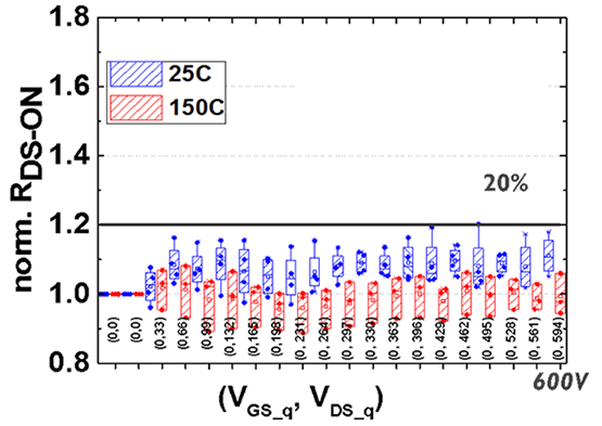
Dynamic RDS-ON dispersion (10µs on – 90µs off)of imec’s 650V GaN-on-Si e-mode device technology measured at 25C and 150C |
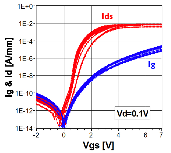
Transfer characteristic of 36mm gate width imec’s 650V GaN-on-Si e-mode transistors |
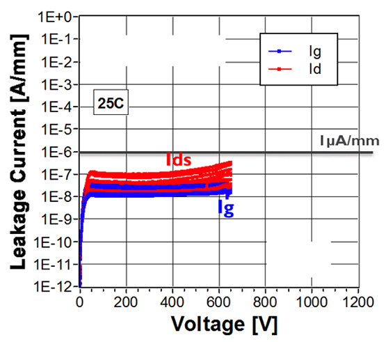
Leakage characteristic at VGS=0V of 36mm gate width imec’s 650V GaN-on-Si e-mode transistors |
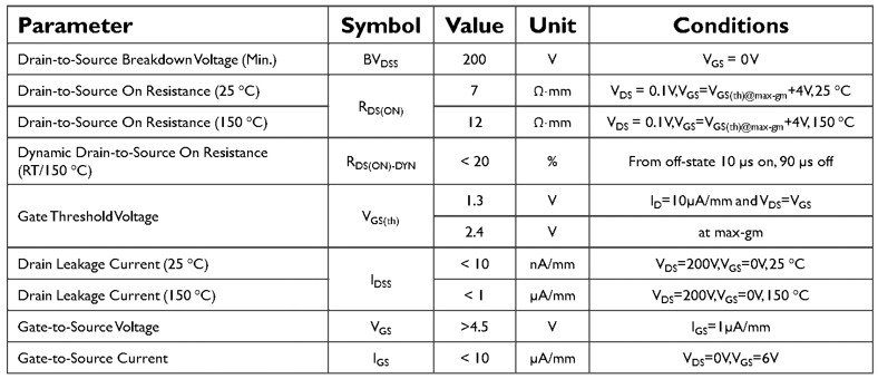
Normalized spec table of imec’s 200V GaN-on-Si e-mode device technology
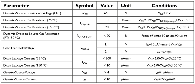
Normalized spec table of imec’s 650V GaN-on-Si e-mode device technology
Typical Output Characteristic and Transfer characteristic of 36mm gate width imec’s 650V GaN-on-Si e-mode device technology
About imec
As a trusted partner for companies, start-ups and universities we bring together close to 3,500 brilliant minds from over 75 nationalities. Imec is headquartered in Leuven, Belgium and also has distributed R&D groups at a number of Flemish universities, in the Netherlands, Taiwan, USA, China, and offices in India and Japan. In 2016, imec's revenue (P&L) totaled 496 million euro. Further information on imec can be found at www.imec-int.com
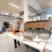
A thermal design specialist at Danfoss Silicon Power describes ways he used FloEFD, a 3D computational fluid dynamics (CFD) program, to dramatically improve efficiency and performance in power-module cooling systems. By: Klaus Olesen
I am a thermal specialist and researcher at Danfoss Silicon Power, a small division of Danfoss Drives that employs around 450 people working in Flensburg, northern Germany. Our group creates only customized products—everything we produce is according to customer specification—power modules and IGBT power modules, as well as MOSFET power modules for automotive and industrial motor drives. We also build power modules and power stacks for wind turbines and solar-power systems.
We use liquid cooling for many of these products because it has heat transfer coefficients that are several orders of magnitude higher than air cooling, enabling much higher power densities and more compact solutions. A product’s lifetime operation and reliability is directly related to temperature management, so we use thermal simulation and analysis software based on computational fluid dynamics (CFD) to optimize our products.
The liquid cooling system for power modules needs to be highly efficient. Typically, the power module is placed on a cold plate (a heatsink with water flowing inside, See Figure 1); a thermal interface material (TIM) is used to fill the gaps where surfaces meet because the surfaces are wavy and uneven. When we used CFD to analyze the materials, we found that 20–30% of the thermal resistance was in the TIM. So, to make our cooling system more efficient, we wanted to remove the TIM from our designs. We believed that if we could eliminate the TIM, we could reduce complexity and increase reliability. These considerations are especially important in applications that need long lifetimes such as wind turbines and electric/hybrid vehicles, where pump-out and dry-out effects of the TIM create problems.
Figure 1: Power module mounted on a cold plate.
When approaching a design like this, one of the most common methods is to have water in direct contact with the power module on the backside using pin fins (Figure 2). Pin-fin coolers are often used in the traction modules for electric car inverters; and although they are very efficient, pin fins have some drawbacks. For example, power modules with pin fins have temperature gradients inside them arising from operational heating. As water gets hotter, the power module’s temperature rises from one end to the other. Also, pin fins are expensive.
Figure 2: Pin-fin cooling system.
Figure 3: The ShowerPower liquid-cooling system.
To create a laminar flow, we designed small channels into the structure. But once we had laminar flow, we then had a buildup of the boundary layer which leads to poor thermal performance. To fix this issue, we applied the hydraulic swirl effect, which eliminated the boundary layer. We then had low pressure drop from the laminar flow and high performance from the swirl effect. An interlaced manifold structure on the backside of the new product also enables customizable, parallel cooling of multiple modules. Rather than creating 7,000 parts and taking three years to test the physical prototypes, we were able to use CFD to optimize the channel geometries (depth, height, length, etc.), for optimal thermal performance in a matter of weeks.
Let’s take a look at a couple of examples of how we used simulation and analysis to optimize the cooling solutions for the power modules provided to our customers. The first example is a wind turbine converter. The customer specification was for differential pressure drop, P3 half-bridge modules at 1,700 V (1,000–1,800 A), with six modules per cooler and one brake chopper (Figure 4).
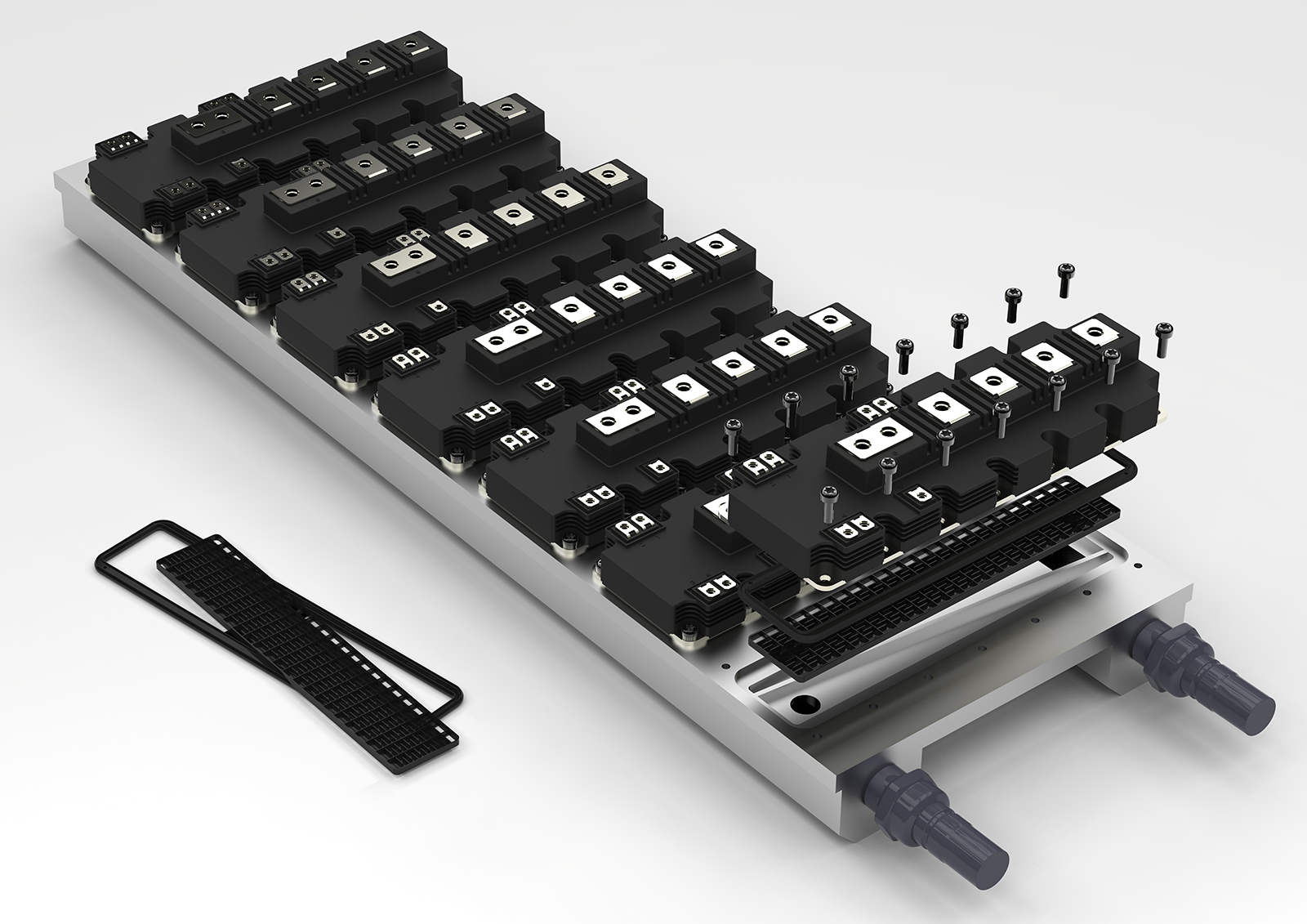
Figure 4: P3 power module for a wind turbine.
We needed to find the right configuration for an optimal design. Wind turbine generators are huge assemblies of large power modules running in parallel, and they need homogenous cooling to be able to operate at the same temperatures. In this case, we used simulation to analyze the hydraulic balancing for multi-bathtub assemblies (Figure 5). Our simulation system incorporates FloEFD, a full-featured 3D CFD analysis solution built into major MCAD systems such as Creo, CATIA V5, Siemens NX, and Solid Edge. FloEFD enables engineers to move CFD simulation into the design process early to examine trends and dismiss less desirable design options. It can help reduce the entire simulation time by up to 75% compared to traditional CFD solutions.
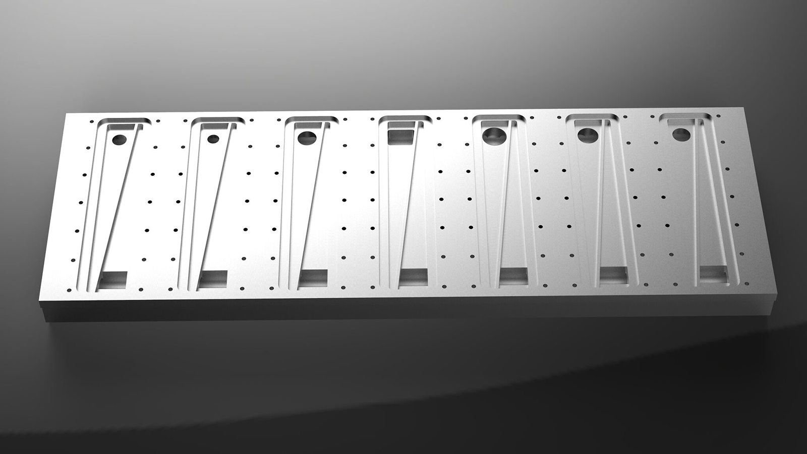
Figure 5: Looking at the optimal configuration for hydraulic balancing of multi-bathtub assemblies.
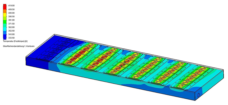
Figure 6: Simulation results for the first hole design configuration.
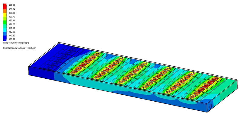
Figure 7: Simulation results for the second hole design configuration.
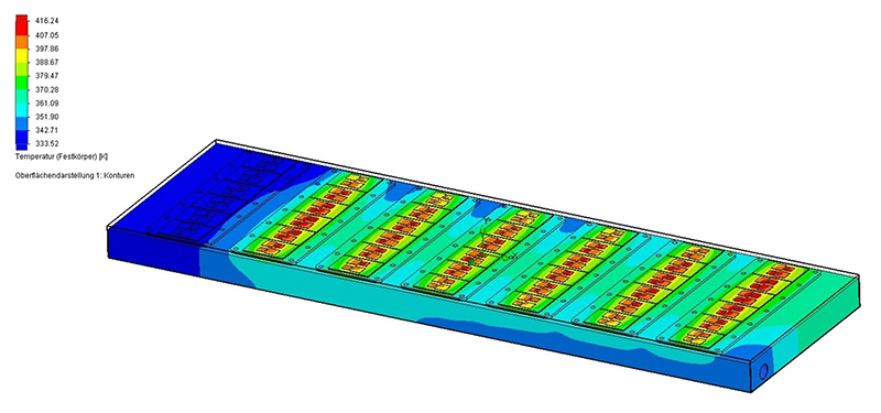
Figure 8: Simulation results for the third hole design configuration.
This example has seven power modules that receive cooling water in parallel. The small holes needed to be adjusted individually to get the same flow rate. We used simulation to analyze the results when varying seven inlet holes. For the first design, we wanted to optimize the cooling system so that the modules have the same temperature. But the result was inhomogeneous; the first module was much hotter than the one next to it (Figure 6).
These results led us to try another design. In this case, the last one was too hot, and the middle one was too cool (Figure 7). The third design was a little bit better (Figure 8). Using CFD, we could run 700 iterations to reach an optimum solution quickly. If we were doing physical prototypes, the cost of the aluminum parts would have been several thousand euros, and it would have taken several weeks to have just one supplied.
The second example is a transfer-moulded, half-bridge module (650 V/800 A, 6 x 6 cm). In this case the module could not be allowed to have more than 100 millibar differential pressure drop. This is a huge challenge; it meant that the cooling of each power module needed to be as good as possible, and the application’s three modules needed to be cooled equally well. The flow rate was lower per area with water temperatures higher. This was a difficult challenge; at times, working with dual heating and struggling to get the right boundary conditions for our simulations that would match the experimental conditions. The boundary conditions for volume flow rates typically were 5–7 L/min per inverter at 70–90 °C. The glycol-to-water ratio was 50/50. Environmental pressure was assigned to the outlet. For Joule heating, self-heating on bond wires and conductor tracks were also considered.
We also wanted to incorporate thermal radiation in our simulations. Because we only supply the one module, one component of a large system, radiation is difficult to take into account when we do not know the rest of the system. We could not have solved it without being able to use CFD combined with our customer’s CAD files.
When developing this new cooling technology, we had to address one of the known challenges of designing large power modules with ceramic substrates that are soldered to a copper base plate. When it is soldered at 250° C, the solder solidifies to 220° C at cool down, and then the ceramic substrate does not shrink because of the low coefficient of thermal expansion of the substrate compared to the copper. This process results in small indentations or depressions on the backside—a few hundred microns deep, which create small gaps through which water can take a shortcut, passing between the baseplate and the plastic cooling module. Because of this phenomena, our colleagues for years had been saying this type of design will never work. So to get around this seemingly impossible problem, we decided to simply include the bypass as part of the system (Figure 9).
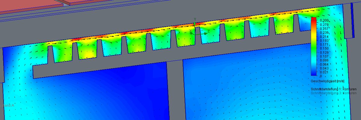
Figure 9: Simulation of using the bypass in the cooling system design.
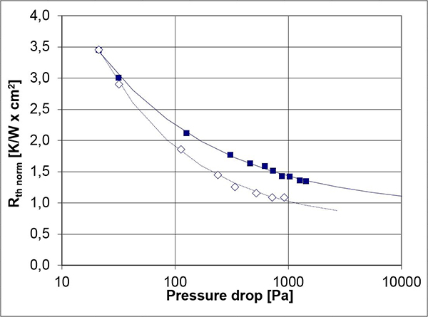
Figure 10: Thermal performance improves while differential pressure drop is reduced.
With this change in approach and some deep analysis, we found that we could actually use the bypass to reduce the differential pressure drop and thermal resistance (Figure 10) for overall improved performance.
Conclusion
One of the benefits of using FloEFD as part of our computational fluid dynamics thermal simulation and analysis is that we can get a deeper understanding of the physics of the systems we are working with. We often receive a STEP CAD file from the customer for each new project, and we cannot edit a STEP file, but this is not an issue for FloEFD, which can work with that file format. CFD programs often have a problem with round and small features, crashing while attempting to mesh them. So typically, I would have to spend two long days of work to remove all the round features before I could run the meshing process. But with FloEFD, I can skip that step; the software ‘eats everything raw’—in other words, as we receive it, and measures it accurately and quickly. My team can use the simulations to separate different physical effects, focus on one and then investigate what happens with that particular physical effect. This allows us to experiment and come up with novel designs that we could only do with a CFD tool that works well in our CAD system, enabling us to collaborate closely with our customers for their custom products.
References
1. Danfoss Silicon Power, siliconpower.danfoss.com/themes/showerpower/#/
2. Mentor-A Siemens Business, www.mentor.com/products/mechanical/floefd/
Author Bio
Klaus Olesen has worked at Danfoss as an R&D engineer since 1990 and has specialized in thermal design for the past 16 years in Danfoss Drives. He holds a number of patents for power modules and thermal cooling technologies. He has a Master’s degree in Physics from Aarhus University, Denmark.
Electric power grids transport energy as alternating current (AC) even though electrical devices typically operate using direct current (DC.) Imec researchers and industry have proposed a different paradigm: the DC Nanogrid, which they believe may reshape future homes and businesses.
For historical reasons, the electricity grid transports alternating current (AC) and so most of today’s buildings are wired to use AC. However, up to two- thirds of electricity consumption in homes and commercial buildings is direct current (DC). In addition, local energy generation with solar panels and battery storage also generates and stores DC. So wouldn’t it make sense to begin equipping buildings with local DC grids? Imec – Europe’s premier research and innovation hub in nano-electronics and digital technologies – dedicated a whole afternoon of its Imec Technology Forum 2017 Belgium conference to this question. Invited speakers from research and industry made a case for the bold move towards setting up commercial buildings and homes with DC nanogrids.
Why we have AC in our homes, and why DC would be better
In the late 19th century there was a dispute between Nicola Tesla and Thomas Edison and their respective backers and financiers. Now known as the ‘Current War’, this contention still largely determines how our energy grids function today. The main dividing question was in which form power would be distributed: AC or DC? Tesla supported high-voltage, longer-distance transport lines with AC and Edison promoted DC with local electricity generation nearby the loads.

More than 100 years ago, both AC and DC power systems were developed, but DC had its limitations, mainly for the efficient distribution of electricity over longer distances. Therefore, AC technology – with the electric current periodically reversing direction – was eventually chosen over DC. One of the main reasons was the ease to adapt voltages by means of transformers. Tesla’s view on electricity took the overhand and persists till today: AC power rings through the public grid, into the buildings, and eventually to the socket.
Johan Driesen, professor at KU Leuven and EnergyVille, pointed out that the electricity landscape is now seeing important changes, changes that are set to revolutionize the picture and turn the scales for DC. “Most important was the advent of LED lighting, which is DC-powered. Then there is the inevitable move towards local electricity generation mainly through rooftop PV panels, which generate DC. Local generation will be made more efficient by local battery storage, again DC. This adds up to a plethora of new household appliances which all run on DC, think of laptops, air conditioning, fridges and all battery-run equipment.”
That begs the question: why not set up local DC networks in residential homes, commercial buildings or even industrial sites?
Johan Driesen: “We have made a modelled cost comparison between buildings that run on either AC or DC, both equipped with PV generation and battery storage. In the AC building, all appliances but also the PV installation and the battery are separately connected through AC/DC convertors. In a DC building, there are only DC/DC convertors and a single AC/DC convertor to make the connection with the grid. This has learned taught us that a DC grid may be 35% percent cheaper in terms of capital cost and 10% percent (less) in terms of electricity consumption. So both financially and in terms of sustainability, local DC nanogrids make a lot of sense. DC nanogrids will be a good fit with future (nearly) zero-energy buildings equipped with integrated PV and battery storage, he added.
This view was backed by Marija Zima, group leader, power & energy systems at ABB Switzerland. “A large share of global energy consumption goes to residential homes and to cars. Technological advances in both these domains will ensure an ever-growing share of DC-native equipment. That is an engineering issue that we must start to tackle today.”

How can we make the world ready for DC nanogrids?
“The concept of equipping our buildings with DC nanogrids is a fairly new one,” says Jef Poortmans, scientific director, Photovoltaics at imec and R&D strategy director at EnergyVille. “We now need to underpin the case with more research and outcome-based experiments. That is why we have made DC nanogrids one of the spear points of EnergyVille, one of the most extensive collaborations in the energy domain in Europe.
“EnergyVille is an association of the Flemish research institutes: KU Leuven, VITO, imec and UHasselt in the field of sustainable energy and intelligent energy systems. Our researchers offer their expertise to the industry and public authorities. The overarching goal is to move towards energy-efficient buildings and intelligent networks for a sustainable urban environment. This includes, for example, smart grids and advanced district heating and cooling. One of the objectives of EnergyVille is to become one of the top five European institutes in innovative energy research. In this context, the center was embedded in major national and international networks right from the start.”
But there is more to organizing a sea change than getting the technology ready and optimized, says Paul Matthijs,. Matthijs is CEO of Niko, a market leader for innovative and smart electricity sockets, switches and home automation. He knows what it takes to get consumers to adapt to a new idea.
“At the end of the day, people like you and me have to foot the bill. And they will only do so if they see clear personal advantages. What we urgently need,” he asserted, “are transnational standards, so that early adopters are not locked into choices that later prove to be wrong. Also, the industry and research has to adopt a user-centric language. Talking about grid balancing and converter losses will not win over many people. Instead, we should prove to people that a DC grid will give them additional comfort, gain them money, and make their life simpler. The current introduction of smart electricity meters, with several standards and an unclear economic picture, could serve as an example and warning.”
What needs to be done on the side of technology?
ITF being is a technology forum, so there were also a number of speakers who presented and discussed technological options for future home grids.
Bart Onsia, innovation program manager for Flanders at imec, looked at how solar energy generation might be much more tightly integrated with buildings. “If we want to curb rising CO2 levels in an environment with a growing electricity demand, we’ll need a much higher deployment and efficacy of PV technology. And as 40% of electricity is consumed in buildings, that is also where that PV technology should be deployed.”
Onsia made a case for building-integrated PV, solar technology as part of the whole building and not only the rooftop, also e.g. on vertical or eEast- and wWest-oriented facades. He presented some technologies that could be mass produced, but that are highly customizable at the same time. Technologies such as woven fabrics as basis to interconnect cells into variable-sized modules, thin-film semitransparent technologies, or smartly wired PV modules that are shadow-resistant. All these technologies have been studied and developed at imec and are now ready to be taken up by the industry.
Moving inside the building, Matthias Strobbe (senior researcher imec – IDlab – UGent ) discussed the lacking lack of interoperability of smart home appliances. He showed how his lab has built a smart home lab in which researchers may test appliances, develop interoperability middleware and model user behavior.
Peter Coenen, senior expert at VITO and EnergyVille, talked about battery storage and the need to develop and incorporate smart battery management systems. “Today the economic case for battery storage is still not always clear,” he said. “We need management systems that do a better job at e.g. monitoring charge levels and times, tracking the state of health of individual batteries, or balancing batteries in an array.” And then there was Joff Derluyn, CTO of Epigan, a spinoff of imec developing gallium nitride (GaN) substrates for high-power switching. “All predictions and trade-offs for future grids depend on how efficient solid-state based power electronics for conversion will be, an efficiency that also depends on the materials used. “GaN is much more up to the task than silicon, but it is also much more expensive. That is why Epigan is developing a compromise: GaN deposited on cheaper silicon substrates. Converters made from these wafers promise not only a higher efficiency, but they will also operate at higher temperatures, allow much higher power density, and have a higher switching speed. These will allow making much smaller converters than is possible today.”

Edison@Home – soon in a theatre near you?
“There is now a better case than ever to go back to Edison’s original proposal for local DC networks,” says Johan Driesen. “But there is still much to consider and organize. Will we use unipolar or bipolar wiring, and what will be the voltages? To test options and see how they work out, we’re setting up a DC nanogrid in one of our Energyville buildings. The building will be powered with solar panels, have battery storage, a bipolar 4-wire grid, and a scalable voltage.”
And for those who can’t wait to revisit the Current Wars, says Driesen, “there is now a movie replaying the Edison-Tesla discussion, with Benedict Cumberbatch as Thomas Edison and Nicholas Hoult as Nikola Tesla. Soon in a theatre near you!”
ITF Belgium is the flagship edition of the worldwide series of Imec Technology Forums. Each year, it rallies experts and visionaries from around the world at a two-day event to discuss the future of technology and how tech innovation can be brought to market.
NXP has released a new line of processors and microcontroller solutions for the IoT, low power requirement designs and high performance multimedia applications. PEW’s Mark Andrews spoke with NXP’s Ron Martino, VP and GM of the company’s i.MX product line, about their new solutions and the company’s nod towards FD-SOI technology.
NXP Semiconductors (Eindhoven, Netherlands) announced in March that it was bringing new processors and microcontroller solutions to market based upon FD-SOI (fully depleted silicon on insulator) technology, supplanting CMOS in wide-ranging applications. The company also announced new development frameworks and SoCs.
NXP subsequently announced that Amazon was utilizing i.MX products in next-generation ‘Alexa’ devices. In a separate announcement the company said that its Android Things platform, utilizing i.MX applications processors, supports the new Google Cloud IoT Core, which is a managed service for securely connecting and managing devices at a global scale.
NXP previously announced that its i.MX 7ULP design would deliver ‘deep-sleep’ suspended power consumption of 15 uW or less: about 17 times better than its previous low-power i.MX 7 devices. Dynamic power efficiency for the new device family is 50 percent better in real-time domains, said the company.
Although NXP’s new product line offers superior performance compared to earlier generations, some industry watchers found the news of NXP’s commitment to a long-range plan broadly migrating design of general purpose processors and microcontrollers from CMOS nodes over to FD-SOI as most significant. What proved to be deciding factors for the company are the capabilities they find in FD-SOI to deliver designs that can provide low power consumption, high efficiency and scalability. NXP indicated that it sees prospects for developing a variety of processor families all from one FS-SOI process node.
NXP’s embrace of FD-SOI began two years ago after Samsung announced ‘dramatic improvements’ in power, performance and efficiency in their process recipe. Earnest development began shortly thereafter; qualification came early in 2016, with the first devices arriving at NXP offices late last year.
For NXP, FD-SOI technology represents what some might characterize as an easy transition from SOI—technology with which their design engineers were already well experienced. Key advantages include the flexibility brought by its back-biasing and forward-biasing techniques. In a nutshell, ‘forward back-bias’ is an ideal way to increase performance, while ‘reverse back-bias’ is an excellent way to reduce leakage.
Power Electronics World’s Mark Andrews spoke to Ron Martino, VP and GM of NXP’s i.MX product line about the new solutions and his company’s commitment to FD-SOI technology.
PEW: Does the switch to FD-SOI for i.MX devices indeed signal a shift to that technology for low-power solutions overall, or primarily for IoT-related applications?
Ron Martino: The choice of 28nm FD-SOI for next-generation i.MX offerings signals a new paradigm (for the) applications processor -- optimization of power, performance and integration for a diverse set of applications. Our low power solutions (i.MX 7ULP), delivering power efficiency for battery operated devices, will concentrate the transistor design and mix to minimize the leakage through Reverse Body Bias (RBB), as well as lowering dynamic power through Forward Body Biasing (FBB). The performance solutions (i.MX 8 and i.MX 8X), targeting optimized power-performance for wired operated devices, will leverage Forward Body Bias for high performance modes, as well as having the ability to achieve extremely low power wait states for efficient system design and operation. In addition, multiple applications will leverage the process’ inherently high immunity to soft errors and latch-up to dramatically improve system reliability.
PEW: Are there other applications for which NXP believes FD-SOI is the ideal tech?

Ron Martino
PEW: Are there other applications for which NXP believes FD-SOI is the ideal tech?
Ron Martino: FD-SOI will benefit many markets targeted by NXP: consumer, industrial and automotive. All three markets require the power-performance benefits. The industrial market will benefit from the significantly improved Soft Error Rates (SER), which can go up to 100x versus bulk, as well as the immunity to latch-up.
PEW: Does NXP favor FD-SOI due to its forward back-bias for a performance increase, while its reverse back-bias is a superior choice to reduce leakage?
Ron Martino: FD-SOI enables a significantly wider range of RBB and FBB compared to bulk technology alternatives. Lower Vmin operation is achievable without the need of additional devices, which add cost and complexity to the technology and integrated circuit development. The basic technology integration has fewer masking steps compared to alternative bulk options, so short cycle times can be achieved in development and manufacturing of product. Lower failure rates can be achieved based on superior immunity to latch-up and SER. Device oxide is thicker than some alternatives in the industry allowing for more reliable solutions for automotive and industrial applications. Analog and RF integration significantly benefits from superior characteristics in gain, noise, and switching. In addition to the above which link to product attributes, there are benefits to internal development efficiency. The wide dynamic range of FD-SOI enables the broadest range of scalable solutions on a single technology platform.
PEW: Does NXP see other benefits that FD-SOI technology offers?
Ron Martino: FD-SOI offers the ability to deliver a full range of new leadership products across the continuum of microcontroller, microprocessor and connectivity offerings. The future integration of disparate technologies such as novel NVM, innovative analog leveraging benefits of FD-SOI and RF capability with leadership low power capability enables NXP to apply its innovative culture to create impactful safe, secure and connected solutions for its customers.
PEW: Does NXP see FD-SOI as a replacement for CMOS in applications outside IoT?
Ron Martino: We do in key areas: Automotive: Cluster, display audio, telematics and V2X applications processor benefits. Also in Industrial: Industrial control, Point of Sale (POS), robotics, industrial transportation application benefits. And in consumer products: Multiple IoT and wearable/portable application benefits.
PEW: The new NXP IoT Framework is said to drastically reduce the ‘time, effort and expertise’ needed to build production-ready IoT systems compared to a system integrator approach. Could NXP please elaborate?
Ron Martino: In addition to the leadership embedded processing and connectivity products that NXP has introduced to the market, it also delivers leadership enablement and solutions around these offerings to improve time-to-market and reduce development efforts for its customers. In particular, NXP is delivering an Integrated Development Environment (IDE) that simplifies system development requiring connectivity (Thread, ZigBee, Wi-Fi Ethernet, NFC), security (secure element, integrated hardware security), embedded processing reference design, and smart device/cloud computing enablement and interoperability.

What does the future hold for SiC device manufacture at Infineon?
With volume production of SiC devices underway, what next for Infineon?
It's no secret that higher efficiency, increased power density and a smaller footprint are just a few advantages that SiC MOSFETs offer over the silicon IGBTs. So as photovoltaic inverter, uninterruptible power supply and electric vehicle charging markets finally look set to adopt the technology, industry players have a raft of products ready.
Rohm recently unveiled an all-SiC, 1200V, 600A power module optimised for inverters and converters in solar power conditioners, UPS, and industrial power applications, just as Wolfspeed claimed its all-SiC 1200V power model had met harsh environment qualification tests.
In the last two years, STMicroelectronics has delivered a series of 650 and 1200 V SiC MOSFETs. And last month, Infineon revealed it had started volume production of its full-SiC module while delivering new module platforms and topologies for its 1200 V CoolSiC MOSFET family.
For Peter Friedrichs, Senior Director of silicon carbide at Infineon, the time is right to ramp up production. As he puts it: "We are seeing a tipping point for certain applications - solar power conversion, UPS and electric vehicle charging - thanks, in part, to a very attractive total system cost."
According to Friedrichs, inductive components make up a relatively large part of the bill of materials in many applications, including solar power conversion.
However, silicon carbide enables higher switching frequencies, allowing the use of smaller external components including inductors and capacitors, saving board space and overall component cost.
"This reduction in the bill of materials was the tipping point for the use of SiC Schottky diodes more than fifteen years ago," highlights Friedrichs. "And these SiC devices were extremely highly priced at the time."
But looking beyond system costs, the time is also right to ramp up production as the industry transition from 100 mm to 150 mm SiC wafers is well and truly underway.

Peter Friedrichs, Senior Director of silicon carbide at
Infineon: "We believe that the playground for GaN HEMTs
600 V while SiC can compete with silicon IGBTs at 1000 V
and above."
However, silicon carbide enables higher switching frequencies, allowing the use of smaller external components including inductors and capacitors, saving board space and overall component cost.
"This reduction in the bill of materials was the tipping point for the use of SiC Schottky diodes more than fifteen years ago," highlights Friedrichs. "And these SiC devices were extremely highly priced at the time."
But looking beyond system costs, the time is also right to ramp up production as the industry transition from 100 mm to 150 mm SiC wafers is well and truly underway.
In May, last year, STMicroelectronics announced it was scaling up its production of SiC MOSFETs and diodes on 150 mm wafers, predominantly to drive down manufacturing costs and deliver volume to automotive industry.
Now, Friedrichs confirms that Infineon has made the transition from 100 mm to 150 mm wafers for SiC diode production.
From word go, the company has also developed its SiC MOSFETs on 150 mm wafers, forging a strong connection between technology development and wafer availability.
And right now, the company is sourcing its 150 mm wafers from a handful of vendors worldwide - 'the known companies' says Friedrichs - that can offer volume capability.
"The move from 100 mm to 150 mm is a major change and as always, some customers are more reluctant than others to change their products, but we are nearly there," he says.
"For 150 mm, we still see slight quality differences from supplier to supplier, whereas with 100 mm wafers quality is comparable," he adds. "But we believe we will move beyond this very soon and it isn't a sticking point at all."
Chasing markets
Infineon now intends to ease its first full-SiC module based on 1200 V MOSFETs - Easy 1B - into volume production this year. This module will target solar, UPS and charging applications.
Meanwhile, a larger module - Easy 2B - will follow, and this version is designed for higher power ratings in target applications. Friedrichs reckons the latest module configurations will also soon be used in industrial drives, medical applications and auxiliary power supplies for the railway sector.
"We have already seen our hybrid modules - which combine silicon IGBTs with silicon carbide diodes - being used in solar power conversion applications, and these will now be partially replaced with the silicon carbide switch," explains Friedrichs. "Silicon carbide is also going to be highly appreciated in the emerging electric vehicle fast-charging infrastructure market, but we do not expect to see modules in actual electric vehicles until at least 2020."
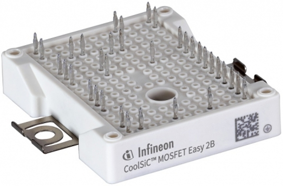
Easy2B in half-bridge topology targets solar inverters, quick-charging systems
and uninterruptible power supply applications.
For now, customer acceptance is not a huge issue. According to Friedrichs, some customers are more conservative than others and wish to see field data first, which can be difficult with a new technology. And while faster switching devices bring EMC issues, the Senior Director is confident the necessary support can be offered here.
Crucially, Friedrichs reckons the company can keep pace with future leaps in demand.
"We expect market growth to be around 20% [year-on-year], which is a lot greater than total power semiconductor growth," he says. "But we have good flexibility regarding volume manufacturing. We already have three and a half million SiC modules in the field - hybrid modules dominate so far - but we expect similar figures for the full-SiC modules as well."
Manufacturing aside, Friedrichs is also certain that SiC very much has its place amongst the rise of silicon semiconductor alternatives.
"We believe, for example, that the playground for GaN HEMTs is very much 600 V while SiC can compete with silicon IGBTs at 1000 V and above," he says.
And looking to the future, Infineon has a roadmap in place for higher voltage systems; Friedrichs expects demand for 1700 V full SiC MOSFET modules to be driven by solar power conversion and traction applications, and eventually 3.3 kV modules will follow.
"We have frequent discussions about 10 kV and 15 kV parts but are still in 'observation mode' for such devices," he says. "We want to understand that there is a real market here, and that this [development] wouldn't be an academic exercise to simply achieve a world record."
The benefits of wireless battery recharging over a distance appeared about as likely as jet packs and flying cars until Dialog Semiconductor and Energous Corporation began their quest to cut the cords.
While consumers clearly love their smartphones, laptops and tablets, they equally detest the tangle of power converters and charger cables cluttering backpacks and briefcases from Bristol to Burbank. This love/hate relationship could be about to change if power technology companies Dialog Semiconductor and Energous Corporation successfully deploy their new WattUp® family of wireless charging solutions.
Wirelessly recharging mobile device batteries is hardly new. Existing wireless solutions typically employ coils to carry power to receiving devices; however, these have their limitations. According to Dialog Semiconductor’s Senior Director of Corporate Strategy, Mark Hopgood, it is precisely those limits that make the solutions developed by Energous Corporation with support from Dialog so compelling. Without charger mats, precise alignment or other persnickety requirements, the WattUp solution offers benefits that Hopgood says consumers expect: no clutter, and more importantly, no wires.
“I think wireless charging has not lived up to a lot of consumers’ expectations. In some cases it can be downright frustrating to find that your device has not charged because it wasn’t placed quite right on the charging mat. We believe this new solution is much closer to consumer expectations – it will be a difference they appreciate when it comes time to buy,” Hopgood said.
Dialog traces its roots back to 1981 and included times as a Daimler Benz AG subsidiary infused with CMOS and semiconductor technology from Silicon Valley’s International Microelectronic Products company; its expertise in power management electronics later extended into smartphones incorporating ARM processors. Work with LED power technology and sensors were later added as the company grew to multiple locations in the UK, Europe, Asia and the US. Dialog’s broad power-focused market appeal eventually led to a relationship with Energous Corporation that began in 2014 and was formalized with a partnership and cash infusion of (USD) $10 million in 2016 to support Energous’ development of its WattUp wireless technology.
Energous developed its WattUp technology that provides over-the-air power at a distance as an alternative to existing wireless recharging techniques including those of other AirFuel Alliance members. Although Energous and Dialog stress the wireless aspect of their technology enabling recharging at a distance, WattUp could be employed to create near field charging mats, but without the precise placement requirements some consumers find challenging.
Both companies believe most consumers will realize additional benefits as longer-distance charging applications become available, such as deciding when a device is ‘refueled.’ Consumers can choose priority devices for recharging, or let anything properly equipped sip power as needed. WattUp receiver technology can be incorporated in a very wide range of consumer products that can ultimately be charged from various types of WattUp transmitters. Even if WattUp devices are positioned in a wireless recharging mat in a near field application similar in appearance to existing systems, Hopgood said Energous’ core technology has important advantages.
“One of the things we looked at comparing coil based tech vs. Energous (WattUp) was the fact that the receiver coils tend to require a large diameter and an added physical dimension—a ‘z’ height thickness. Because of this, (coils) are often too big to be integrated into many products that could benefit from wireless charging. But if we reduce the footprint at the device level—which WattUp technology does, this translates into the antenna becoming nothing more than the tracking on a PCB; we can even use the same antenna for charging that you would use for Bluetooth,” Hopgood said.
Besides eliminating the coil that other wireless charging technologies depend upon, Hopgood said Dialog and Energous have worked to move from discrete components to integrated semiconductors that further reduce space and increase efficiency. At the same time, WattUp software is designed to ensure that charging waveforms are dynamically directed, focused and controlled via proprietary algorithms; for mid field and far field charging applications consumers can choose various control options including recharging when electricity rates are lowest.
Dialog and Energous have moved forward with their plans to further miniaturize key component technology with the announcement in January of their first jointly produced integrated WattUp wireless power transmit (Tx) IC, the DA4100. This new System-on-Chip (SoC) integrates an ARM Cortex-M0 along with RF power generator, power management and secure element functionality into a single 7x7mm device. It also features on-chip DC-DC conversion and embedded software, providing seamless integration to Dialog’s SmartBond™ family of highly integrated, low power BLE SoCs. The new DA4100 minimizes board space needed to implement, enabling smaller charging transmitters and simplifying overall design-in requirements.
Gordon Bell, VP of Marketing at Energous, said that the DA4100 is the backbone of all WattUp transmission designs including the near field transmitter that the US Federal Communications Commission (FCC) recently approved.
“We are engaged with a large number of product companies currently looking to incorporate the WattUp receiver technology into their devices. These companies would typically bundle a WattUp near field transmitter along with their product to offer devices that are charged wirelessly,” said Bell.
Bell elaborated that while many end use designs are possible using WattUp receiver technology, Energous and Dialog expect that WattUp-enabled transmitters will most likely appear in future consumer markets focused on two primary applications: standalone and embedded transmitters.
“Standalone transmitters have a single function to allow for wireless charging to WattUp-enabled receivers. A standalone near field transmitter would likely be a small charging pad included inside the box of many small electronics (replacing the USB cord and power brick typically bundled inside today). A standalone mid field transmitter may be incorporated into the dashboard of a car or may be a small device that sits on your desktop, allowing for charging in the 2-3 foot range. A standalone far field transmitter may look similar to a Wi-Fi access point installed on the wall or ceiling, allowing for wireless charging at up to 15 feet,” Bell explained.
“Embedded transmitters would be part of another product. For instance, the near field transmitter technology may be embedded into the top of a Bluetooth speaker, allowing you to charge small electronics simply by placing them on top of the speaker…. A desktop assistant type of product may offer mid field WattUp charging to other devices nearby. And the bezel of your TV may one day offer far field WattUp (utility), charging its own remote control, game controllers and other devices within 15 feet of your TV. All of these implementations would use the DA4100 as the backbone of the wireless charging function,” he concluded.
As the WattUp technology moves from development stages to design-in with lead customers, Dialog’s Mark Hopgood said that the change from coil-based wireless charging approaches and other technologies to antennas working with directed RF signals will affect consumer purchasing. The degree to which a consumer has adopted mobile devices and uses them away from mains power supplies could be decisive.
“There are so many gadgets that are a slave to a socket; WattUp technology has the potential to change the way we use our battery powered devices…let’s look at near field; at face value one might think that our technology doesn’t really add much advantage, but actually when you go from a coil to an antenna based system, you dramatically reduce the footprint and the cost, so just doing that opens up a whole new category of devices. Also, RF is less precious about positioning the device on the charge mat.
“The paradigm shift may occur that when you are using a device, you are sending just enough energy over the distance (using WattUp technology) to keep the devices topped-up. This could be done constantly…so you can reduce the size of the battery, or you can simply not worry about charging them again by keeping them under a managed constant charge. That is where the paradigm shift will occur that the consumer will appreciate,” he concluded.
While both Dialog and Energous could not share details regarding the original equipment manufacturers that are currently working to incorporate WattUp technology into future end user devices, they did indicate that product sampling and qualification tests were underway. The companies expect consumer devices incorporating WattUp wireless charging may begin appearing in some global markets later in 2017.
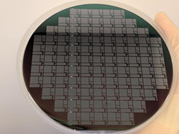
First patterned SiC wafer from the New York Power
Electronics Manufacturing Consortium. [NY-PEMC]
In a breakthrough for power MOSFET qualification, the New York Power Electronics Manufacturing Consortium (NY-PEMC), led by the State University of New York Polytechnic Institute (SUNY Poly), recently produced patterned wafers in its SiC process line at SUNY Poly’s Albany, NY, campus.
Dr. Jeffrey C. Hedrick, Vice President of SUNY Poly, "This means we are up and running, our tools are up and running, and our engineers and scientists are now working hard to fabricate these advanced devices."
It all started in 2014, when the General Electric Company (GE) partnered with SUNY Poly to build a state-of-the-art 150 mm process line for silicon carbide MOSFETs and diodes.
Forming the New York Power Electronics Manufacturing Consortium - NY-PEMC - with SUNY Poly, GE provided more than $100 million in intellectual property, while overall investment in the consortium, including support from New York State, reached $500 million.
Then, come 2015 and another $100 million in New York State funds, GE and SUNY Poly revealed plans to establish a power electronics packaging facility at the Computer Chip Commercialization Center (Quad-C) located on SUNY Poly’s Utica campus.
And with Danish power module manufacturer, Danfoss Silicon Power, recently joining GE and SUNY Poly to set up SiC power module packaging operations here, NY-PEMC looks set to become the 'silicon carbide corridor' of North America.
Hedrick certainly thinks so. Heading up both the wafer fabrication and packaging arms of NY-PEMC, he highlights how the manufacturing consortium will help provide much needed jobs and revitalise the economy of Upstate New York.
GE will fabricate cutting-edge SiC chips that will then be assembled and packaged by Danfoss for integration into systems. Fabrication capabilities will top 15,000 wafers a year, and with Danfoss earmarked to operate the only domestic high-volume packaging centre in a burgeoning US market, the future for NY-PEMC looks bright.
"GE and Danfoss are our core members, and we expect to add other key partnerships in the near future," says Dr. Hedrick. "We're equipped to easily run 15,000 wafers a year, which is more than sufficient for the next three years, and we have the expansion capabilities to increase this figure to 50,000 when the market ramps up to higher volumes."

Latest developments
In recent months, activities at NY-PEMC's wafer fabrication arm have focused on scaling up its baseline process flow to manufacturing readiness. The process flow includes technology developed at the GE Global Research Center in Niskayuna, New York. And as Hedrick points out: "GE has been continually working with us to transfer technology from its research centre to our line in Albany."
Right now, the wafer fabrication facility is in its final stages of ISO 9001 certification in a SiC-dedicated Class-1 capable cleanroom. All tools, including photolithography, reactive ion etching, metallization, metrology, measurement, in-line electrical test and more, are nearing full installation. And the consortium's team of engineers intends to have the process flow verified and qualified - to automotive AEC-Q101 reliability specifications - by the end of this year.
"We're focusing on process setup and verification right now," explains Hedrick. "But very soon we will be able to fabricate qualified MOSFET devices with unmatched reliability."
Indeed, come 2018, 1.2 kV MOSFET fabrication will be well underway, and this is just the beginning. Hedrick and colleagues intend to offer 1.7 kV MOSFETS shortly thereafter, and then higher voltage devices and integrated circuits by 2020.
What's more, the tools installed in the SiC process line are 200 mm-capable equipment from top-tier manufacturers, and as Hedrick points out, have been 'chucked down' to support 150 mm wafers.
"The industry is currently transitioning to 150 mm substrates and will eventually transition to 200 mm substrates," highlights Dr. Hedrick. "In a few years from now when the 200 mm substrates are technically and economically viable, we will be able to chuck our tools up at a low cost."
"As the market ramps up, we're going to be ready,” he adds.
Meanwhile, activities are also well underway at the packaging center at Quad-C in Utica. The site will house manufacturing lines for industrial, transportation, and automotive applications, while additional lines will be devoted to research and development, and prototyping of new modules and power blocks.
"We have a very aggressive schedule to get the packaging facility set up for Danfoss and we are ordering many of the custom tools right now," says Hedrick. "These have a lead time of up to eight months and we'll get many of them by the end of this year."
"We'll start installing these tools as soon as we can, and have the first three lines qualified in 2018," he adds.
So with all systems go for the next few years, what does the longer-term hold for NY-PEMC? Hedrick, for one, hopes to continue extending what he describes as the power electronics ecosystem within NY-PEMC.
Gallium-nitride-on-silicon (GaN-on-Si) technology is maturing at a rapid pace and is expected to be adopted soon in different markets. Applications mainly include high-voltage power switching and power conversion, RF power amplifying and sensing. But for certain applications, the technology has a considerable disadvantage: multiple GaN devices (such as high electron mobility transistors) have limited capability for monolithic integration on the same GaN-on-Si wafer. Imec researchers therefore take a different approach and combine, for the first time ever, GaN-on-SOI (silicon on insulator) technology with trench isolation to achieve monolithic integration. They presented their results at the 2017 Workshop on Compound Semiconductor Devices and Integrated Circuits (WOCSDICE) and the work has been published in IEEE Electron Device Letters.
[p-GaN HEMTs monolithically integrated on a GaN-on-SOI wafer.]
GaN-based power devices
GaN is anticipated to be the next generation power semiconductor. With a higher breakdown strength, faster switching speed, higher thermal conductivity and lower on-resistance, power devices based on this wide-bandgap semiconductor material can significantly outperform the traditional Si-based power chips. Initially, the development of GaN-based technology focused on high-voltage (600V) power-switching applications and lower-voltage DC-DC converters. As such, the first-generation GaN-based power devices will play a key role in the power conversion within battery chargers, smartphones, computers, servers, automotive, lighting systems and photovoltaics. Meanwhile, new opportunities in other application areas are emerging, including RF power amplifiers for future 5G wireless communication and GaN-based gas- and biosensors.
In absence of viable low-cost GaN bulk substrates, GaN is grown on a variety of substrates, the most popular being sapphire, silicon carbide (SiC) and Si. Si substrates have become attractive for GaN growth because of their larger wafer diameter (200mm and higher) and lower cost perspective, and the ability to use standard semiconductor processing lines.
The benefits and challenges of monolithic integration
Today, fabrication of most GaN power systems is based on a multi-chip solution. This means that different GaN-based components (or devices, such as high-electron mobility transistors (HEMTs)) are assembled as discrete components on a common PCB. This solution is however complex and expensive. An interesting alternative is to monolithically integrate GaN power devices on one single chip, resulting in a smaller and less complex overall system. Also, monolithic integration promises a better control of parasitic capacitances and inductances, and a better power conversion efficiency.
A half bridge, one of the most common switch circuit topologies used in power electronics today, is a typical example of a convertor topology that would benefit from monolithic integration. It consists of a low-side switch (with the source at a low potential) and a high-side switch (with the source at a high potential), connected in an electrical circuit. During operation of the device, the two switches are turned on and off complementary to each other. The switches therefore need to be biased differently, and this requires isolating the substrates of the high-side and low-side devices.
Achieving monolithic integration of different components on GaN-on-Si is however very challenging. In GaN-on-Si devices, lateral isolation of the different components is provided by an isolation implant or a mesa etching process. Vertical isolation is however only partially realized by a high-resistive buffer. In this topology, the devices still share a common conductive Si substrate that can only be referenced to a single potential at a time.
Top view of the fabricated device. A box-like isolation
structure is created around each HEMT device.
Exploring GaN-on-SOI for monolithic integration
To achieve monolithic integration of GaN-based power devices, imec is exploring alternative integration and isolation approaches. One of the roads towards device isolation is to grow GaN on SOI wafers and use trench isolation to isolate the devices.
In a SOI wafer, a layer of silicon dioxide (SiO2) is sandwiched between two Si layers. The general objective of this technology is to improve the insulating characteristics of the wafer. SOI technology is also being explored as a substrate for growing GaN, mainly to investigate the potential benefits in terms of GaN crystal quality. Growing GaN on SOI is different from growing GaN on Si, with more layer parameters to tune. Also, dedicated strain engineering is required to control stress during the epitaxy.
Imec researchers have for the first time combined GaN-on-SOI technology with trench isolation for the monolithic integration of GaN-based devices. The aim is to isolate the devices by trench etching through GaN and Si into the SiO2 buried layer, and as such demonstrate the monolithic integration capabilities of GaN-on-SOI technology for e.g. half bridge applications. The devices used in this study are enhancement-mode (e-mode) p-GaN HEMTs. These transistors use a p-type gate and operate in normally off (or e-mode) mode, an operation mode that is preferred over ‘normally on’ for power efficiency and fail safety.
Device fabrication and trench etching
Imec researchers grew a GaN epi-stack epitaxially on a 200mm SOI wafer (Si(100)/SiO2/Si(111)) using metal-organic chemical vapor deposition (MOCVD). The stack consists of an AlN nucleation layer, an (Al)GaN buffer layer, a GaN channel layer, an AlGaN barrier layer and a Mg-doped p-GaN layer. Delicate strain engineering was performed to control the stress built up in the wafer during growth, resulting in a GaN-on-SOI wafer with a controlled warpage and good mechanical strength. In a next step, e-mode p-GaN HEMTs were processed and a TiN/p-GaN stack was used for the gate.
The HEMTs were then isolated horizontally as well as vertically by the combination of nitrogen implantation isolation and by trench etching through the (Al)GaN/Si(111) to the SiO2 buried layer. This way, a box-like isolation structure is created, surrounding each HEMT with an insulating dielectric.
(a) Horizontal breakdown of the trench isolation and (b)
vertical breakdown of the SiO2 buried layer on the 200mm
GaN-on-SOI at 25°C and 150°C.
Transfer characteristics of a HEMT at
150°C (a) with common Si substrate
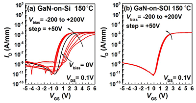
biased from -200 to 200V (GaN-on-Si) and (b) while
simultaneously biasing the neighboring
Si(111) HEMT layer at different voltages (GaN-on-SOI).
The effectiveness of GaN-on-SOI device isolation
The p-GaN HEMTs on GaN-on-SOI have been fully qualified for 200V switching applications. Both the horizontal breakdown voltage of the trench isolation and the vertical breakdown of the SiO2 buried layer reach ~500V at 150°C.
The effectiveness of the device isolation becomes clear from the transfer characteristics of a HEMT device on GaN-on-SOI. These characteristics show the ID vs. VGS behavior of one device while the neighboring HEMT device is biased differently. The HEMTs are shown to be very robust when the substrate of the neighboring device is biased between -200V and 200V. This is in clear contrast to the performance degradation of devices on GaN-on-Si observed in similar experiments.
With these results, imec researchers have demonstrated for the first time that using GaN-on-SOI in combination with trench isolation is a promising approach to monolithically integrate GaN power systems on the same wafer.
The research on GaN-on-SOI is part of imec’s Industrial Affiliation Program on GaN power devices. Within this program, imec takes today’s GaN-on-Si technology to a higher level of maturity and reliability, and explores new concepts for next-generation GaN technology. In this explorative track, imec focuses on new integration and device technologies, including novel substrates (such as GaN-on-SOI) and alternative isolation techniques (such as junction isolation and trench isolation).
The research is also carried out in the frame of the European ECSEL PowerBase project. PowerBase aims at developing the next-generation energy-saving chips based on materials such as GaN. Under the coordination of Infineon, the 39 project partners prepare these semiconductors for mass industrial use in smartphones, laptops, servers and many other applications. Within this project, imec looks beyond traditional substrate technologies for GaN-based devices, and explores novel isolation technologies. The PowerBase project receives funding from the Electronic Component Systems for European Leadership Joint Undertaking under grant agreement No 662133.
Want to know more?
| Publisher/Editor | Jackie Cannon jackie.cannon@angelbc.com +44 (0)1923 690205 |
 |
|---|---|---|
Web Developer & Campaign Assistant |
Owein Mason |
|
Technical Contributor |
Mark Andrews |
|
| Sales & Marketing Manager | Shehzad Munshi shehzad.munshi@angelbc.com +44 (0)1923 690215 |
|
| Sales Executive | Jessica Harrison Jessica.Harrison@angelbc.com +44 (0)2476 718979 |
|
| Circulation Director | Jan Smoothy jan.smoothy@angelbc.com |
|
| Chief Executive Officer | Stephen Whitehurst stephen.whitehurst@angelbc.com +44 (0)2476 718970 |
USA Representatives
Tom Brun, Brun Media E: tbrun@brunmedia.com +001 724 539-2404
Janice Jenkins E: jjenkins@brunmedia.com +001 724-929-3550
Director of Logistics - Sharon Cowley sharon.cowley@angelbc.com +44 (0)1923 690200
Design & Production Manager - Mitch Gaynor mitch.gaynor@angelbc.com +44 (0)1923 690214
Directors - Bill Dunlop Uprichard - Chairman, Stephen Whitehurst - CEO, Jan Smoothy - CFO,
Jackie Cannon, Scott Adams, Sharon Cowley, Sukhi Bhadal, Jason Holloway.
Published By
Angel Business Communications Ltd, Hannay House, 39 Clarendon Road,
Watford, Herts WD17 1JA, UK. T: +44 (0)1923 690200 F: +44 (0)1923 690201 E: ask@angelbc.com
Angel Business Communications Ltd, Unit 6, Bow Court, Fletchworth Gate, Burnsall Road,
Coventry CV5 6SP, UK. T: +44 (0)2476 718 970 F: +44 (0)2476 718 971 E: info@angelbc.com
PEW Magazine is published four times a year on a controlled circulation basis. Non-qualifying individuals can subscribe at: £105.00/€158 pa (UK & Europe), £138.00 pa , $198 pa (USA). Cover price £4.50. All information herein is believed to be correct at time of going to press. The publisher does not accept responsibility for any errors and omissions. The views expressed in this publication are not necessarily those of the publisher. Every effort has been made to obtain copyright permission for the material contained in this publication. Angel Business Communications Ltd will be happy to acknowledge any copyright oversights in a subsequent issue of the publication. Angel Business Communications Ltd © Copyright 2016. All rights reserved. Contents may not be reproduced in whole or part without the written consent of the publishers. Power Electronics World - ISSN 2398-9815
