
Building on the success of its predecessors, the fourth Photonic Integrated Circuits (PIC) International Conference (26-27 March) pinpointed the most promising opportunities accross industry. More than 700 attended the co-located conferences that focused on advances in PICs, compound semiconductors and the future of advanced sensor solutions.
As conference Co-Chairs Dr. Michael Lebby and Dr. Bill Ring note in their wrap-up article, the PIC International Conference continues to exceed expectations. Hundreds of attendees filled meeting spaces. As photonic integration and silicon photonics (SiP) technologies continue to mature, interest in the technology also grows. PICs are seeing wider adoption while more research efforts into hybridization and new materials are expanding what PICs can do in wider markets.
If you were unable to join us in Brussels, be sure to read the event summary article from our conference chairpersons. Some of the best in our industry were honored with 2019 PIC Awards – see their profiles in a separate article. Two notable PIC honorees are Dr. Graham Reed, a professor at the University of Southampton and leading pioneer in silicon photonics (SiP). We have an in-depth look at Reed’s CORNERSTONE programme and its growing MPW and training programs. Also honored was Dr. Martin Schell, the Executive Director of Fraunhofer HHI (Berlin) and Chair of Optic and Optoelectronic Integration at the Technical University of Berlin. He is a regular contributor to PIC magazine; we have included one of his articles that details some of the Institute’s latest advances.
Also in this PIC Magazine is a look at work being done at the Hong Kong University of Science and Technology to grow InP-based lasers on precisely oriented silicon. If this research proves manufacturable it could help remove one of the barriers to more seamless monolithic integration. In a different look at lasers for silicon photonics we have an article from the Samsung Advanced Institute of Technology describing new SiP lasers that do not require insulating intermediary layers.
We also have an article from imec (Belgium) discussing a unique approach using SiP micro mirrors to miniaturize the high-caliber performance of Raman spectroscopy desktop-size instruments for the development of new handheld Raman spectroscopes. While we can’t say whether a Raman spectroscope might be an option for future smartphones, imec’s researchers are proving that integrated photonics and silicon photonics are just beginning to show their capabilities across wider swaths of photonics applications.
We hope you enjoy this edition of PIC Magazine and look forward to seeing you at PIC International 2020 in Brussels.
ficonTEC Service GmbH and Coherent Solutions, New Zealand, have entered into a collaborative partnership to advance electro-optical measurement capability for use in volume testing within the manufacturing cycle of integrated photonic devices (PICs).
As optical and electrical technologies become more miniaturized, complex, and increasingly integrated with one another’s underlying architecture, the more inefficient and frustrating it is for process engineers to implement separate electrical and optical test and qualification procedures. To avoid this, engineers require fully-automated systems that can perform complex precision alignment and assembly, as well as combined electro-optical I/O measurements for complex integrated photonic devices – from singulated dies, through to wafer-level and even up to fully-packaged devices.
According to Ignazio Piacentini, Business Development Director at ficonTEC, “Wafer-level testing of PICs differs substantially from that of conventional semiconductor wafers and requires the integration of three major ingredients: Firstly, high-accuracy, sub–µm optical positioning with fast-active alignment capabilities. Secondly, some form of combined electro-optical probe head, and thirdly, modular high-channel-count instrumentation. ficonTEC and Coherent Solutions already provide the necessary capabilities for the first and last ingredients, and together we are actively researching electrical/optical probe head concepts.”
Coherent Solutions’ broad portfolio of photonic test and measurement instruments includes a line-up of modules for the popular PXI platform that leverage National Instruments’ established LabVIEW graphical programming environment. As ficonTEC’s PCM (ProcessControlMaster) software is also based around LabVIEW, integration of the two is seamless and enables the creation of sophisticated and fully-automated test solutions to match individual requirements.
Alternatively, to achieve the same goal within non-LabVIEW and alternative instrumentation environments, Coherent Solutions additionally offers the same optical measurement capability in a range of compact, modular benchtop and IOT-focused test equipment that can be equally well interfaced to ficonTEC’s process control software. Either approach can be flexibly used by manufacturers to speed up development and production of the latest photonic integrated circuits and devices.
Andy Stevens, CEO of Coherent Solutions says, “The last 20 years of investment into technology for optical communications is now spawning new capabilities and products in new applications and markets, which in turn encourages further development and innovation. We are fortunate to support this innovation and are incredibly excited to work with ficonTEC on new automated test and measurement solutions for manufacturers. Our complementary product platforms and design philosophies enable rapid customization and deployment and provide a clear upgrade path as technology advances and products evolve. For customers, this increases ROI and helps them bring new products to market faster and cheaper. Together, we will provide customers with unique products and unrivalled value and support.”
Torsten Vahrenkamp, CEO of ficonTEC Service added, “The collaboration with Coherent Solutions could not come at a better time, as a number of our current activities are geared to further improving performance and capability for our new, next-generation assembly and test systems. By integrating Coherent Solutions’ innovative optical instrumentation and software into our modular machine architecture and process control software, respectively, we take a significant step forward in our continued and growing support for integrated photonics developments worldwide.”
The two companies are initially focusing their sights on manufacturers of modules and components for telecom and datacom, and on systems for testing high-density VCSEL systems as used in 3D optical sensing/imaging applications, such as for automotive LIDAR and for face recognition modules found in smartphones.
ficonTEC and Coherent Solutions will display the initial results of this collaboration with a live demonstration of a fully-automated photonics test system at NIWeek in Austin, TX/USA, from May 20-23, and again at Laser World of Photonics in Munich, Germany, from June 24-27, 2019.

Researchers at Cardiff University have shown tiny light-emitting nanolasers less than a tenth of the size of the width of a human hair can be integrated into silicon chip design.
The photonic band-edge lasers can operate at superfast speeds and have the potential to help the global electronics industry deliver a range of new applications – from optical computing to remote sensing and heat seeking,
“This is the first demonstration that shows how photonic band-edge lasers can be integrated directly on patterned silicon-on-insulator platforms,” said Diana Huffaker scientific director of Cardiff University’s Institute for Compound Semiconductors (ICS). Huffake specialises in nanoscale epitaxy, fabrication and optoelectronic devices.

“Silicon is the most widely used material in semiconductor industries. However, it has been difficult to integrate compact light sources on this material. Our research breaks through this barrier by developing extremely small lasers integrated on silicon platforms, applicable to various silicon-based electronic, optoelectronic, and photonic platforms.”
The paper, 'Room‐Temperature InGaAs Nanowire Array Band‐Edge Lasers on Patterned Silicon‐on‐Insulator Platforms', has been published in Physica Status Solidi - RRL.
Wyn Meredith, director of the Compound Semiconductor Centre, a Joint Venture between IQE Plc and Cardiff University, said: “This research will have long-term implications in the rapidly expanding field of photonics, with a particular emphasis on driving commoditisation of high volume, high specification optical components for mass market communications and sensing applications.“
Cardiff University, IQE and the Compound Semiconductor Centre are members of CS Connected – the world’s first hub for compound Semiconductor technologies based in South Wales.
The ICS is due to move to a new state-of-the-art Translational Research Facility on Cardiff Innovation Campus in 2021.
The Ferdinand-Braun-Institut, Leibniz-Institut für Höchstfrequenztechnik (FBH) is showing its range of services at Laser World of Photonics in Munich from June 24-27, 2019. At the joint Berlin-Brandenburg stand, the institute will present current developments, from chips and modules with and without fibre coupling to live demonstrators. At the accompanying CLEO conference, FBH will be represented with 16 scientific contributions.
LiDAR demonstrator: stand-alone, PC-controlled pulsed laser source
As part of 'Research Fab Microelectronics Germany', FBH is presenting a live demonstrator for pulsed laser sources, which allows flexible adjustment of pulse duration and intensity. Visitors can use a tablet to change the desired parameters and monitor the results in real time on screen.
With its PLS flex, FBH offers laser sources that deliver pulses in the range from 200 ps to 20 ns. The systems can be equipped with diode lasers of various wavelengths (630 - 1180 nm) and power ranges. Laser diodes, which are wavelength stabilised at 905 nm, achieve output powers of up to 100 W at ambient temperatures of up to 85degC. This makes them suited for use in LiDAR systems. FBH offers the chips in a complete development environment with driver electronics and control software.
The compact turnkey laser system for Raman measurements is equipped with a monolithic Y-dual-wavelength diode laser, which alternately emits light at two slightly different wavelengths. The system allows very fast measurements using Shifted Excitation Raman Difference Spectroscopy (SERDS). The spectral distance of both wavelengths can be adjusted via micro heaters above the DBR gratings, which define the wavelength. If the systems are complemented with a suitable power supply, spectrometer, data acquisition and software interface, they can be used for on-site measurements. In-house developed, portable systems have already been successfully used for measurements on food, soil, plants and human skin.

In a recent paper in Phys. Status Solidi A, Chinese researchers have demonstrated light emission from a silicon p‐channel MOSFET with a 6μm effective gate length that is operated as a three‐terminal gate‐controlled LED.
Using a photon‐emission microscope with a detector responsive to the range of 200–1000 nm, they measured emission spectra in the range of 400 to 900 nm which includes visible light radiation.

The team, led by Kaikai Xu at the State Key Laboratory of Electronic Thin Films and Integrated Devices in the University of Electronic Science and Technology of China, say the fabrication of the device is fully compatible with CMOS processing procedures.
Since the MOS‐like diode uses the field effect induced by the gate for modulation of the diode's space charge electric field (and hence the optical output from the LED), the modulation speed for visible and infrared bands can attain high frequencies in the GHz range.
Such high frequencies represent a significant leap in silicon electro-optic modulator performance for future optoelectronic interconnects using standard CMOS processes.
The lifetime of the MOS-capacitor LED should be controllable via the capacitor discharge time. In other words, the Si gate-controlled diode LED operates on the principle of the MOS-capacitor and not on standard p-n junctions. In contrast to the lifetime of carriers in the depletion region, the MOS-capacitor discharge time also determines the modulation in the reverse-bias silicon p-n junction with gate control.
Light generation from a Si‐LED provides a way to manufacture all‐silicon monolithically integrated optoelectronic systems composed of CMOS transistors and Si‐LEDs fabricated on the same chip.
'Silicon MOS Optoelectronic Micro‐Nano Structure Based on Reverse‐Biased PN Junction' by Kaikai Xu; Phys. Status Solidi A March 2019 https://doi.org/10.1002/pssa.201800868
Lumerical, a developer of photonic design and simulation tools and Luceda Photonics, developer of IPKISS, a reference platform for Integrated Photonic design and photonic PDKs have announced the immediate availability of a new photonic flow that integrates Lumerical’s FDTD Solutions photonic simulator and Luceda’s IPKISS. These products, familiar to photonic component designers, create a complete flow linking Lumerical and Luceda’s powerful PIC design frameworks, providing designers with the choice to use their favored tools at each stage in their design flow.
Responding to multiple customer requests, Luceda Photonics and Lumerical are committed to integrated photonics designers and developed a link between IPKISS and Lumerical FDTD solutions. The link enables component designers to combine IPKISS PCells with simulation recipes to ensure that components are simulated in Lumerical FDTD Solutions using validated methods on 3D structures that match the fabricated device. Both IPKISS PCells and the simulation recipes are written in Python enabling designer control of the PCell and the associated simulation methodology. The designer can ensure consistency between layout, fabrication process and the generated simulation results that can be further used in the IPKISS and Lumerical design solutions.
Prof. Wim Bogaerts said “At Ghent University we have been interfacing IPKISS and Lumerical for several years now and we are enthusiastically using it for both research and teaching. We are very happy to learn that there will be an official link between IPKISS and Lumerical, and we’re looking forward to enjoy the benefits of this collaboration”.
Erwin De Baetselier, Luceda CEO said “We are really excited about our new collaboration with Lumerical. We are particularly thrilled about using Lumerical’s Python API. IPKISS fully embraces the Python ecosystem and through this new link Lumerical and Luceda Photonics provide the first complete design platform that is completely scriptable from Python.”
James Pond, Lumerical Founder & CTO remarked, “Integration with Luceda is a consistent request from many photonic component design customers. This integration with Luceda, a leader in Python-based mask layout of photonic designs, expands the ecosystem for designers using familiar tools, and further demonstrates our commitment to the Python community.”
Infinera and Fastweb, a major Italian telecoms operator, have announced the successful demonstration of 500 gigabits per second (500G) single-wavelength service connectivity in a production network using Infinera’s configurable technology on the Groove platform. The high-speed optical transmission demonstration, the first in Italy, spanned over 180km on Fastweb’s low-latency long-haul backbone network, between Milan and Turin.
Conducted over Fastweb’s live fibre route between Milan and Turin, the 500G single-wavelength trial demonstrated Fastweb’s capability to easily and efficiently scale its infrastructure network to meet the increasing bandwidth demands of its end-user customers. The trial was implemented over Fastweb’s existing optical infrastructure without special amplifiers, tuning, or changes.
“Providing our customers with resilient, high-quality, and innovative solutions is in Fastweb’s DNA,” said Andrea Lasagna, CTO, Fastweb. “As the market for high-performance long-haul transport continues to grow at an accelerated pace, a scalable and simple network approach is required to satisfy the growing demand for bandwidth. This trial confirms the outstanding performance provided by Infinera’s innovative solution, which enables us to deliver a best-in-class customer experience at the highest transmission speeds.”
Infinera’s 7300 Multi-Haul Transport Platform, mTera Universal Switching Platform and Groove 600G technology are part of Fastweb’s backbone network spanning over 650 nodes and providing the flexibility and future development and delivery of a range of programmable high-speed end-user services at 400G, 500G, and up to 600G. Infinera’s solution enables Fastweb to scale internet exchange point capacity up to 24 terabits per second, while offering ease of deployment and network investment efficiency.
“We are pleased to extend our technology partnership with Fastweb to bring the benefits of cutting-edge coherent optical transmission to their customers,” said Glenn Laxdal, senior VP, product line management, Infinera. “Our ability to introduce higher-speed transmission over existing infrastructures is a key part of our mission to help our customers to effectively meet their increasing bandwidth needs.”
Infinera has announced that Cyxtera Technologies, a secure infrastructure company, has deployed the Infinera Groove Network Disaggregation Platform to support delivery of secure and reliable high-speed data centre interconnect services.
The Infinera Groove solution enables Cyxtera to cost-efficiently scale optical interconnect capacity between its data centre facilities within major markets while meeting the business-critical, low-latency and secure performance demands of its enterprise and service provider customers.
Cyxtera Technologies operates over 50 data centres in major cities around the world, providing more than 3,500 customers with a secure global platform for mission-critical applications and systems.
“We continue to invest in best-in-class technology that supports the performance and security requirements of enterprise-grade connectivity,” said Damion Lackamp, senior director, Interconnection Products at Cyxtera Technologies. “As we expand our data centre facilities, the Infinera Groove solution provides the capacity, efficiency and security to boost the performance of our network infrastructure in a highly compact form factor.”
“With a highly compact and plug-and-play architecture, the Infinera Groove provides Cyxtera a proven foundation for programmable high-speed transmission, including a path to 600G,” said Pete Dale, VP, Cloud and Content Sales, Infinera.
Ayar Labs has announced that it has secured additional funding to fuel its growth as it drives to productize its TeraPHY optical I/O chiplets and SuperNova multi-wavelength lasers in 2019. The funding comes on the heels of the Optical Fiber Conference (OFC), where there was significant industry focus on the need for integrating silicon photonics based optical interconnect into semiconductor packages – a technique that promises to dramatically improve application performance, significantly reduce power consumption, and reduce overall datacenter platform costs for the Artificial Intelligence, High Performance Computing, Cloud, and Telecom markets.
“Silicon Valley Bank (SVB) has a long history of supporting promising technology companies,” said Lafe Vittitoe, Managing Director at Silicon Valley Bank. “Ayar Labs has everything we look for in an investment -- differentiated technology that addresses a large market opportunity, strong management and technology teams, and committed investors. We look forward to a long and fruitful relationship with Ayar Labs.”
The funding, which totals $3 million, comes in the form of a flexible draw down term loan and will be used on specific capital and manufacturing related expenditures as Ayar Labs ramps sampling and production. “SVB is a strategic long-term partner on our journey to bring our revolutionary technology to market,” said Charles Wuischpard, CEO of Ayar Labs. “Our customers and partners are excited at the progress we’re making; SVB’s investment will fuel our growth and accelerate our volume product introduction.”
Ayar Labs is also pleased to announce that it has been awarded a DARPA grant as part of the “Photonics in the Package for Extreme Scalability” (PIPES) program, a research initiative that seeks to develop high-bandwidth optical signaling technologies for digital microelectronics. Through the grant, Ayar Labs will work to accelerate the adoption and integration of the Advanced Interface Bus (AIB), a royalty-free high-bandwidth electrical interconnect standard, which will be used to link third-party chips to TeraPHY.
Additionally, to support its growing design win activities, Vladimir Stojanovic, a co-founder of Ayar Labs and Associate Professor of Electrical Engineering and Computer Science at the University of California at Berkeley, will be joining Ayar Labs in a full-time capacity to lead system architecture.
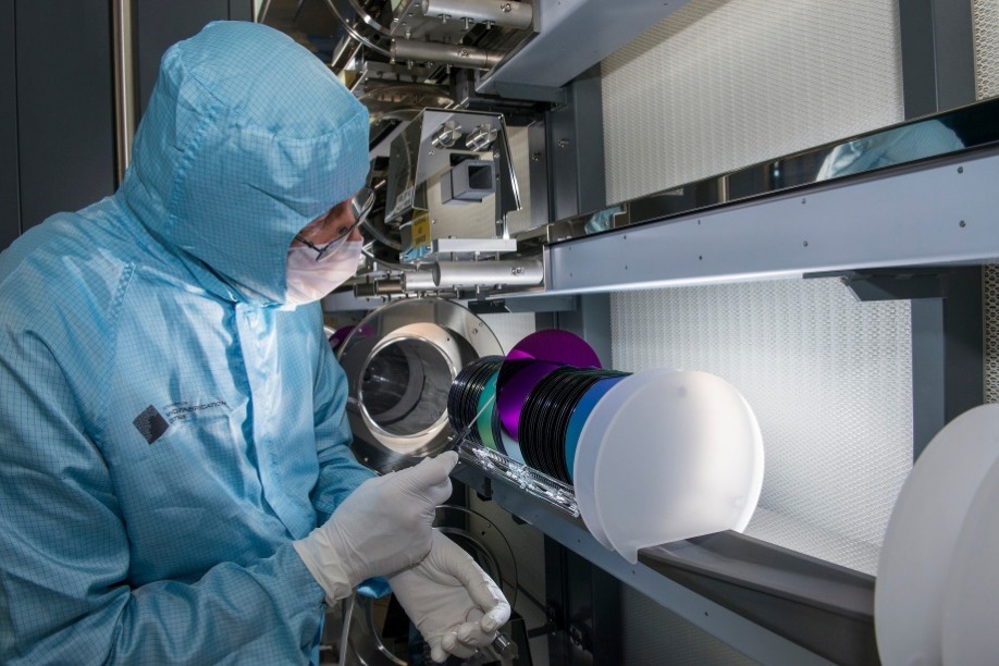
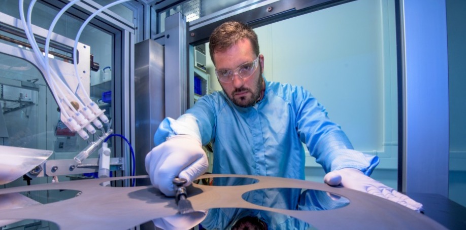
IQE has announced that its recently constructed Newport Mega Foundry has received its first mass production order from its leading existing VCSEL customer.
The achievement of full product qualification status is the result of extensive quality and process audits by the customer and their end OEM, as well as exhaustive product qualification trials including full reliability testing. Qualification of further tools is in progress and is expected to complete over the coming months.
In addition to the qualification with this customer, further VCSEL product qualifications are at advanced stages with more than ten other customers, two of which are expected to reach a successful conclusion over the next few weeks.
Customer feedback from the additional qualifications confirms the superior quality and performance from the new facility.
The Newport Mega Foundry is the largest outsource epi facility for advanced compound semiconductors globally and has been under construction for the last 18 months. It currently has ten large-scale production MOCVD tools installed, with space for up to an additional 90 tools. The manufacturing facility also houses an extensive suite of highly advanced wafer characterisation tools to ensure outstanding, world-class wafer quality.
The first ten tools are dedicated to 6 inch VCSEL production for end applications that include 3D sensing, high-speed datacoms, Advanced Driver Assistance Systems (ADAS), LiDAR, proximity sensing and Time of Flight (ToF) systems.
The market for VCSELs is expected to grow rapidly over the coming years as 3D sensing is installed across multiple user platforms, including facial recognition, world facing cameras for Augmented Reality (AR) and 3D photography, security cameras, industrial sensing and heating, ADAS, LiDAR, high speed datacomms and proximity sensing.
Drew Nelson, CEO and president of IQE commented: "I am very pleased to announce IQE receipt of full product qualification status from our leading VCSEL customer, and the first order for mass production from our new Mega Epi foundry in Newport.
"IQE has invested heavily, along with help from the Cardiff City Region Deal (CCR), to build the worlds largest outsource epi facility, demonstrating our commitment to providing the capacity required for large scale deployment of VCSELs and other Compound Semiconductor (CS) products, as the CS industry moves through a real inflection point in volume manufacture.
"IQE is committed to leadership of this mass CS scaling, offering a unique range of wafer products and complementary technologies, enabling our customers to introduce disruptive products to the end marketplace. We have a powerful and extensive roadmap for VCSEL technology, which we believe will help the acceleration of the deployment of VCSELs across many end applications".
The Laboratory for Nanoscale Optics at the Harvard John A. Paulson School of Engineering and Applied Sciences is rapidly running down the checklist to develop ultra-efficient integrated photonic circuits. First, they developed a technique to fabricate high-performance optical microstructures using lithium niobate. Then, they designed an integrated frequency converter, an integrated modulator and a platform to store light and electrically control its frequency in an integrated circuit. Most recently, they designed on-chip, electronically driven frequency comb.
Now, the team of researchers — led by Marko Loncar, the Tiantsai Lin Professor of Electrical Engineering and Applied Physics at SEAS — has developed a chip-scale frequency comb system that can not only generate a comb, but also manipulate it on the same chip.
“Before this research, once we generated a frequency comb on a chip, we had to transfer the signals out of the chip and use off-chip components for further manipulation of the signals, which are usually bulky and expensive,” said Cheng Wang, co-first author of the paper, former postdoctoral fellow at SEAS, and now Assistant Professor at City University of Hong Kong. “Now, we can integrate all these additional functionalities onto the same chip as the comb generator, potentially realizing many different comb applications all in one chip.”
Optical frequency combs are lasers that emit multiple frequencies (colors) of light simultaneously, each precisely separated like the tooth on a comb. The researchers were focused on generating a specific type, known as a Kerr frequency comb, which has a range of applications in everything from optical clocks and spectroscopy to telecommunications and quantum information processing. While these frequency combs have been generated on-chip before, researchers have struggled to also integrate the components needed to manipulate the comb.
That’s where lithium niobate come in.
Loncar’s lab is pioneering the use of thin-film lithium niobate as a platform for integrated photonics. Its unique electro-optical properties make it possible to both generate the frequency comb on chip and manipulate it.
“This is the first time a Kerr frequency comb has been generated on a lithium niobate platform, and the first time that Kerr comb generation, filtering and modulation were all realized on the same chip,” said Cheng.

“We’ve shown that it is possible to integrate distinct photonic functionalities on a monolithic integrated lithium niobite chip, which could lead to a new generation of microcomb applications in spectroscopy, data communication, ranging and quantum photonics,” said Loncar, senior author of the study.
The Harvard Office of Technology Development has protected the intellectual property relating to this project. The research was also supported by OTD’s Physical Sciences & Engineering Accelerator, which provides translational funding for research projects that show potential for significant commercial impact.
This research was co-authored by Mian Zhang, Mengjie Yu, Rongrong Zhu and Han Hu.It was supported in part by the National Science Foundation, the DARPA SCOUT program, and the Harvard University Office of Technology Development Physical Sciences and Engineering Accelerator. The research was published in Nature Communications.
Synopsys has announced that PLASMOfab, a research project funded by the EU innovation program Horizon 2020, has been successfully completed to enable mass manufacturing of high-performance plasmo-photonic components. Launched in 2016, the project has brought together leading industrial partners and top-ranked academic and research institutes in the photonic integrated circuit (PIC) and opto-electronics value chain, including PhoeniX Software, now part of Synopsys' Photonic Solutions.
The three-year research project has significantly advanced the state of the art in PICs and CMOS-compatible plasmonics for optical data communications and biosensing for point-of-care applications. PLASMOfab has developed CMOS-compatible plasmonics to consolidate advanced PICs with electronic ICs in volume manufacturing. The project focused on CMOS-compatible metals and photonic structures that are harmonically co-integrated with electronics using standardized CMOS processes. As part of project validation, the PIC platform was used along with advanced peripherals to develop predominant functional modules with unprecedented performance.
A key project achievement was the development of a groundbreaking ultra-compact plasmonic transmitter, which has a footprint of 90 x 5.5 µm² to transmit 0.8 TBit/s (800Gbit/s) through 4 individual 0.2 TBit/s transmitters. The project also demonstrated CMOS-compatible plasmonic waveguides with the lowest possible losses, as described in Nature's Scientific Reports in September 2018.
"PLASMOfab's main goal has been to address the ever increasing needs for low energy, small size, high complexity and high performance mass manufactured PICs," said Nikos Pleros, assistant professor at the Aristotle University of Thessaloniki, Greece. "We have achieved this by developing a revolutionary yet CMOS-compatible fabrication platform for seamless co-integration of active plasmonics with photonic and electronic components."
As a result of the PLASMOfab research, two new companies have been launched to commercialize the new technologies:
bialoom Ltd will further explore plasmo-photonic biosensors in multichannel and high-sensitivity point-of-care diagnostics by combining plasmonic sensors with integrated Si3N4 photonic functionalities, electrical controls, biofunctionalization techniques, and microfluidics.
Polariton Technologies Ltd. specializes in new photonic and electronic technologies for the testing, sensing, and telecommunications market. Their energy efficient and low-footprint plasmonic modulator will convert microwave signals to optical signals.
"We expect that further development of CMOS-compatible plasmonic components with CMOS fabrication processes and photonics technologies will demonstrate plasmonics' clear advantages in PICs," said Dr. Dimitris Tsiokos, principal researcher at the Aristotle University of Thessaloniki. "When the best of all three worlds of plasmonics, photonics, and electronics converge in a single integration platform, PICs with unprecedented performance and functionality will be realized, targeting a diverse set of applications and industrial needs while meeting mass production requirements."
"We are pleased to have been working closely with the partners in this project and especially with AMO and ams to develop R&D PDKs for the new PLASMOfab integration technology," said Twan Korthorst, director of Synopsys' Photonic Solutions. "The PDKs are supported by our PIC design platform, which provides the industry's only full design flow from photonic device level to PIC to system levels."
The 2019 PIC International Conference honored outstanding innovators and excellence across the photonic integrated circuits ecosystem with its third annual PIC Awards presented recently in Brussels, Belgium. Honorees received awards based upon thousands of votes cast by persons working at institutes, universities and the global photonics industry to honor the best in PIC research, product and manufacturing equipment development, materials science and leadership.

Accepting the award on behalf of Prof. Reed was Dr. Callum Littlejohns from the University of Southampton’s silicon photonics programmes.
Professor Graham Reed, University of Southampton, was recognized for his foundational contributions to silicon photonics (SiP) and continuing leadership across the industry. He is presently the Deputy Director of the Optoelectronics Research Centre (ORC) and Director of CORNERSTONE—a rapid prototyping, multi-project wafer (MPW) programme also housed at the university that benefits companies and researchers developing new photonic integrated circuits (PICs). The group’s fabrication capability is funded by the Engineering and Physical Sciences Research Council (EPSRC), and collaboratively supports photonics research and manufacturing development programmes in the UK.
Upon winning the award Reed said, “I’m delighted and honoured to receive this award, especially because it was voted for by the silicon photonics industry. Given the buoyant field in which we all work, with so much talent around, it’s a testament to the great job the CORNERSTONE team have done at Southampton.” He added that while the PIC Award is tied to his pioneering SiP work, and in particular the CORNERSTONE project, the field itself and core photonic integration technologies grew as collaborative efforts utilizing II-VI / III-V materials and fabrication technologies.
Reed has dedicated much of his professional career to developing devices that today play a pivotal role in the growing photonics integration industry. He established the first Silicon Photonics Research Group in 1989 at Surrey, later moving programme components to Southampton. A noteworthy outgrowth of his early work was the establishment of the first silicon photonics company, Bookham Technology, which was led by former student, Dr. Andrew Rickman, now CEO of Rockley Photonics. Bookham is now part of Lumentum Holdings, a leading supplier of integrated photonics products to telecom and datacom networks. Amongst many accomplishments in silicon photonics, Reed’s team pioneered the pre-emphasis technique; the first 1 GHz modulator design and the first depletion modulator design that evolved into an industry standard. The team also pioneered industry-leading efforts that include creating the first 40GB/s modulator with high extinction ratio; the first 40Gb/s polarisation independent modulator; the first slow wave modulator, and the first 50Gb/s modulator.
CORNERSTONE has scheduled MPW runs throughout the year, with the next being on their SOI 500 nm platform with a June announcement of the design rules. This MPW run will be followed by a 220 nm SOI platform opportunity that has an August announcement. Check the organization’s website for further details at www.cornerstone.sotonfab.co.uk, or send an email to this address: cornerstone@soton.ac.uk.

Martin Schell was recognized for a professional career dedicated to the advancement of optical science, photonic integrated circuits (PICs), and related technologies essential to present and future high speed data, telecom and video applications. He is chairperson for Optic and Optoelectronic Integration at the Technical University of Berlin and Executive Director of the Fraunhofer Heinrich Hertz Institute, also in Berlin. He is a board member of the European Photonics Industry Consortium (EPIC), as well as OptecBB (Competence Network for Optical Technologies in Berlin/Brandenburg, Germany), and a member of the Photonics21 Board of Stakeholders. Under his direction, the Photonic Component Department (PC) researches optical chip designs and photonic integrated circuits (PICs) for 100Gbps (and beyond) data transmission, detection and sensor applications.
Schell has successfully lead several photonic integrated circuit programs from idea to installation in the field. According to colleagues, he always attempts to be a voice of reason when it comes to evaluating various photonic integration approaches and their economic potential.
Together with international partners from research and industry, Fraunhofer HHI works across the whole spectrum of digital infrastructure – from fundamental research to the development of prototypes and solutions. The institute participates in the standardization of information and communication technologies and creates new applications together with industrial partners.
The Fraunhofer HHI focuses on 10 to 100Gbps transmission in the field of high-performance telecom components. In the area of mobile broadband systems, the organization concentrates its development activities in the areas of signal processing, wireless links and system optimization. Fraunhofer HHI also focuses on optical wireless communications to enable high-speed, short-range links within network systems, especially in environments where electromagnetic compatibility and security are of special concern.
Other primary Fraunhofer HHI research topics are in the area of video- and audio-coding and transmission. The Fraunhofer HHI makes a significant contribution in the fields of greater efficiency in compression methods, autostereoscopic 3D displays and in the integration of real and virtual worlds for immersive multimedia applications.
Best New PIC-Enabled Product or Achievement in Non-Optical-Fibered Modules
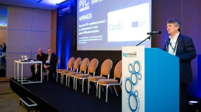
CARDIS, a €3.6 million EU-funded project that is part of the Horizon 2020 program, was recognized for its use of silicon photonics (SiP) as a means to support the early detection of cardiovascular disease (CVD). Partners within the consortium developed a new photonics-based, non-invasive test to screen for CVD that is showing promise in early clinical trials. The CARDIS effort was coordinated by SiP specialists at imec in Belgium. The team has developed a handheld laser Doppler vibrometry (LDV) prototype that has been used successfully in initial clinical trials. Other key partners include the medical device developer and manufacturer Medtronic; researchers at Ghent University in Belgium; the Tyndall National Institute in Ireland; Queen Mary University of London, and the University of Maastricht in the Netherlands.
Identification of individuals at risk of CVD at its earliest stages allows for intervention to halt or reverse the pathological process, according to researchers. Assessment of arterial stiffness by measurement of aortic pulse wave velocity (aPWV) is included in the latest guidelines for CVD risk prediction. Prior to the development of the CARDIS prototype, no medical instrument has been available to screen large populations based on the measurement of aPWV due to the high cost and difficult operational procedures needed with legacy instruments. The goal of CARDIS is to change this situation by providing a cheaper, PIC-based device to measure patients’ aPWV by operators needing only modest levels of training; this is expected to help reduce overall medical costs and risks to patients’ long-term health.
The prototype device has proven to be easy to use in a clinical feasibility study involving 100 patients. The quality of the device readings was found to be very good. In carotid-femoral PWV measurements (the so-called ‘gold standard’ to estimate arterial stiffness,) the performance of the PIC-based device was found to be as good as that of commercial PWV-measurement devices, according to initial tests. The CARDIS device is now undergoing further evaluations to help simplify testing and operational procedures; another clinical study is planned at the Academic Hospital of Maastricht.
To make a PWV measurements, a very low-power laser is directed towards the skin above an artery. A patient’s heartbeat pattern is then determined based upon the Doppler shift of the beam reflected by the skin. At the heart of the multi-beam LDV system is a silicon photonics chip designed by the Photonics Research Group team at Ghent University that was prototyped using imec’s in-house silicon photonics pilot facility.
Best New PIC-Enabled Product or Achievement in Optical-Fibered Modules
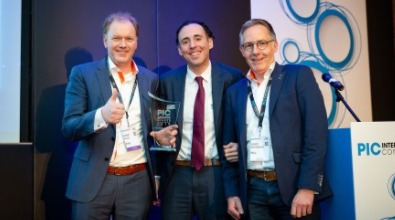
PHIX Photonics Assembly was honored for its continuing efforts to automate and simplify test, assembly and packaging (TAP) systems for photonic chip manufacturing. PHIX was founded in 2017 by LioniX International. PHIX offers a cost-effective manufacturing service for photonic integrated circuit (PIC)-based modules in large volumes. PHIX is located at the High Tech Factory in Enschede, the Netherlands. PHIX offers assembly services for all three major PIC technology platforms (InP, Si and TriPleX) and is specialized in hybrid integration of multiple PICs in one module, both with optical fiber interfaces as well as free space optical interfaces through micro optical components.
At the time of its founding, PHIX said it would work in close cooperation with the Fraunhofer Project Center on packaging standards for high-volume manufacturing of integrated photonics modules, and with PhoeniX Software (now a division of Synopsys) in developing the appropriate photonic design kits dedicated to assembly and packaging.
Hans van den Vlekkert, the CEO of LioniX International who helped to established PHIX, emphasised the need for a strong regional ecosystem for integrated photonics, where education, development, production and volume production go hand in hand.
“We have seen accelerated growth of integrated photonics market over the past year, especially for the demand of devices that are based on our low-loss TriPleX platform. We have delivered many prototypes to international customers and anticipate volume demand for the PIC modules … which requires an efficient organisation, such as PHIX B.V., where the infrastructure and production flow are tailored to achieve cost-effective assembly and packaging of PIC modules.”
Best Achievement in PIC Platform
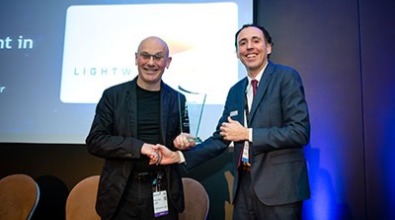
Lightwave Logic was honored at the third PIC Awards for development of its 100GHz photonic integrated circuits (PICs) platform based on the company’s high-performance Perkinamine™ polymer materials which target the insatiable demand for fast data communications in the multi-billion-dollar telecom and data markets supporting media streaming, AI (artificial intelligence) and IoT (Internet of Things).
With photonics continuing to penetrate deeper into networking applications, polymers are seeing increased applications due to their unique material properties, compatibility with existing fabrication methods, equipment and devices. Polymers also have the potential to impact non-communication markets such as sensing, LIDAR/automotive, and medical/healthcare.
Unlike most polymers used in passive photonics today, Lightwave Logic’s Faster by Design™ technology is a very high-speed active integrated optics technology that has similar capabilities to semiconductor platforms but is capable of extension to higher speeds and lower electrical power consumption.
The PIC International Conference created its PIC Awards to put the spotlight on innovation and key industry advances in photonic integration through platform development, manufacturing, design, packaging and device characterization. Lightwave Logic participates on all these fronts including engineering and synthesis of its polymer materials. The company recently announced a new material with double the electro-optic activity as its prior material. Increased electro-optic activity is important as it directly affects modulator drive voltages and consequently enables lower power consumption. Results achieved to date point to the great remaining untapped potential of engineered polymer materials.
Dr. Michael Lebby, CEO of Lightwave Logic, accepted the award at the ceremony in Brussels. He noted, “I am truly proud and privileged to be able to accept an internationally recognized award for our polymer technology platform on behalf of all of Lightwave Logic. The team has worked very hard in developing innovative, high performance, power-efficient materials and devices for the internet, and this award is a testament to the quality of their work.”
Lightwave Logic, Inc. is a development stage company moving toward commercialization of next generation photonic devices using its high-activity and high-stability organic polymers for applications in data communications and telecommunications markets. Photonic electro-optical devices convert data from electric signals into optical signals. For more information about Lightwave Logic, please visit the corporate website at lightwavelogic.com.
Best Achievement in PIC Development
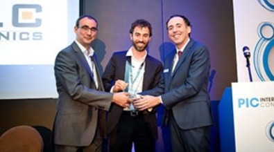
VLC Photonics was honored for its outstanding contribution to the creation and support of the ecosystem for fabless PIC development. The company has been serving the industry for the last eight years by providing photonic integration services to many customers in different markets. In this period, VLC Photonics has pioneered the design house business model for photonics, building a brand that is well recognized as a symbol of expertise, professionalism and independence. Its technical works (when publication is possible while adhering to confidentiality agreements with its customers,) have been published in more than 50 scientific conferences, industrial magazines and peer-reviewed journals, including the prestigious Nature and Optica.
The company has designed and taped-out photonic integrated circuits at 20 different foundries on all the main material platforms, including silicon photonics, silicon nitride, indium phosphide and PLC. Many photonic building blocks have been developed and validated into proprietary libraries and Process Design Kits (PDKs), including arrayed waveguide gratings, multi-mode interference couplers, Echelle gratings, ring filters, tunable lasers, etc. Its designs are now enabling commercial optical transceivers and interconnects, fiber sensor interrogators, quantum cryptography devices and many more.
Recently, VLC Photonics trained a team and invested more than 600,000 euros in equipment to better serve its customers at the chip characterization and testing stages. Such tests are still one of the main bottlenecks when moving from prototyping to production, and VLC Photonics has successfully achieved becoming a photonic test house that supports the full design-to-test cycle in a flexible and semi-automated way. Moreover, VLC Photonics’ characterization capabilities span from the infrared range, typical of telecom and datacom applications, down to the near infrared and visible wavelengths, which are more frequently used in biophotonic, LiDAR or quantum applications.
VLC Photonics has also been reported upon in more than eight market reports from different sources as one of the key players of the ecosystem. The company and its founders have received many awards and recognitions in the last years. It has partnered with the main photonic EDA companies, the largest foundries and pioneering photonic packaging houses as well. These partnerships enable offering turn-key solutions to customers in a seamless and efficient way. Its customer base ranges from small technology start-ups to large Fortune 500 corporations, and has been steadily growing and consolidating along the years.
Building on the success of its predecessors, the fourth Photonic Integrated Circuits (PIC) International Conference pinpointed the most promising opportunities for this industry. More than 700 attended the co-located conferences that focused on advances in PICs, compound semiconductors and the future of advanced sensor solutions.
Conference Co-Chairs, Dr. Michael Lebby and Dr. Bill Ring, praised the leadership and organization of the fourth photonic integrated circuits (PIC) International Conference that took place 26-27 March in Brussels. 2019 marked the fourth consecutive year of growth, with more than 700 attendees and 70 sponsors joining to hear from industry leaders focused on advanced technologies driving the future of global business.
"We have just finished the fourth annual PIC International Conference, and again like in 2018, it surpassed everybody's expectations. But what's more, folks are now recognizing throughout the value chain, from wafers to epitaxial growth, devices, packaging, modules and systems, to social media that PIC International is the conference to attend if your interest is photonic integrated circuits (PICs). We again filled all of our seats, and like last year folks from CS International and SSI attended the PIC sessions. Our annual PIC awards generated nearly 10,000 online votes and the winners in six categories were announced at the end of Day One by the European trade association, EPIC. In (our) humble opinion, this was the best PIC International event to date, and achieved not only world class speakers, world class presentations, but also world class networking during the exhibit hours, breaks, and meal events,” remarked co-chairmen, Dr. Michael Lebby and Dr. Bill Ring following the event.
The prestigious PIC industry awards entered their third year. Winners were voted for by the PIC industry and include the following honorees:
Individual Awards:
1) PIC Lifetime Achievement award - Professor Martin Schell
2) PIC Individual Contributor award - Professor Graham Reed
Company Awards:
1) Best Achievement in PIC development - VLC Photonics
2) Best Achievement in PIC platform - Lightwave Logic
3) Best new PIC-enabled product or achievement in optical-fibered modules - PHIX
4) Best new PIC-enabled product or achievement in non-optical-fibered modules: H2020-Project CARDIS http://www.cardis-h2020.eu/
In 2019 more than 700 delegates attended two days of jam-packed (and at times, standing room only) sessions on photonic integrated circuits (PICs) that focused not only on innovative technology, but how PICs could alleviate major headaches that optical networks, datacenters, telecommunications systems and related applications see today. Many talks focused on how PICs could be implemented into novel and innovative applications to move the industry forward while at the same time providing the long-term scalability needed to grow an industry for decades to come. As in 2018, one of the biggest drivers for PICs are fiber optic communications for datacentre interconnects. Facebook spoke about the huge opportunities for innovative solutions within their datacentres that addressed high speed, low power consumption, innovative packaging (via co-packaged solutions), reliability, and cost effectiveness. Companies like Facebook are looking for PIC leadership, quality and reliability in their bid to replace slower, lower bandwidth legacy systems that are already creating data bottlenecks.
There were also talks that explored PIC based technologies outside of fiber optics including biologic and health monitoring/diagnoses, medical, sensing, and LiDAR for automotive applications. One of the most promising segments for PICs is 3D sensing, especially face recognition for mobile phones.
This year's conference brought together luminaries of the PIC industry who participated in two panel sessions: the first on Day One addressed high volume, high performance PICs for fiber communications; the second on Day Two explored the merits of manufacturing PICs using shared foundries and pilot lines from all over the world. Panel members represented PIC design and manufacturers from Japan, the USA and Europe. The panel sessions generated interesting themes such as: PICs for datacentres are already entering service; PICs for telecom are a quickly growing opportunity; PICs for non-communications markets also rapidly expanding.
In a sense, the Day One panel emulated what was being said in the PIC talks: New and innovative solutions to PIC packaging are urgently needed. One solution advocated by panelists is generally referred to as co-packaging - a way to package PICs along with electronics as a means to bring the photonics closer to the electronics and thereby achieve higher switch capacities on a line card in a datacentre. Today, the popular solution is to use pluggable transceivers mounted into a faceplate. Speakers said that for tomorrow, they supported solutions to use not only on-board optics, but co-packaged optics driven by PIC technological platforms.
The Day Two panel session focused on PIC foundries and their eco-system. Panelists were questioned on the business aspects of running a PIC foundry, the volume needed for sustainability, and the impact on MPW (multi-project wafers) or sharing costs so that SMEs (Small and Medium-sized Enterprises) can participate. Comparisons were made with the silicon industry that has developed a strong foundry model over the past 30 years. In photonics, and in particular PICs, the photonics foundry model is just developing and still in its infancy. Panelists discussed the merits of what photonic PIC foundries need to assist in success. One area that was frequently raised during both panel session discussions and in foundry-based presentations was volume. While GaAs VCSEL-based PICs are experiencing consumer success and volume activity with the application of structured light for optical sensing, other PIC-based applications are not consumer based and as such similar high volumes have yet not materialized. Silicon photonics has the potential to drive costs very low with 200mm and 300mm wafers and is still looking for a high-volume vehicle. Indium phosphide PICs are on smaller wafers (75mm and 100mm) and also would like to see high volumes and even larger format wafers at 150mm.
The conference discussed in detail incumbent PIC technologies such as InP and GaAs, as well as Silicon Photonics (SiP), Polymer Photonics (PP), and Dielectric Photonics (DP). Silicon photonics continues to grow in use and popularity with companies such as Intel, Hewlett Packard Enterprise, AIM Photonics, and Rockley Photonics showing the impact of silicon economics. Infinera and Ciena showed very high-performance PIC results on indium phosphide, while companies such as Broadex and LioniX showed significant progress with dielectric photonics. Lightwave Logic also reported their results with very low voltage, very high bandwidth polymer device designs.
The conference also discussed both datacentre and telecommunications opportunities for PICs with forecasts for new architectures, standards, technologies and cost expectations. The latest results in the PIC field were also presented and showed a significant performance upgrade towards transceivers at 400Gbps while some speakers spoke about a future aiming towards 800Gbps, 1600Gbps and beyond.
There were a number of exciting sessions, including those that emphasized the role of software tools for modelling, simulation, and production. One session discussed improvements in PIC infrastructure for designing and manufacturing robust and reliable PICs using the latest in advanced software design tools. This was supported by many PIC talks that addressed PDKs and other metrics needed to quickly grow PIC markets.
This year, new and innovative talks discussed how PIC-based technologies can enable new products that have smaller form factors, low power, and high performance, which is becoming especially important for hand-held battery powered diagnosis and health monitoring products. CARDIS, an EU-funded program and 2019 PIC Award winner, is one example of using SiP PICs for medical diagnosis.
Conference speakers also addressed new opportunities that can arise as the result of designing PICs for telecommunications and datacom applications and the ways in which these telecom/datacom PIC designs could easily be applied to medical, measurement, automotive, and other industrial applications. Perhaps by next year's PIC International Conference we will see the first products emerge in these new market segments.
Conference speakers also shared the good news that a number of emerging opportunities for PICs will be high volume, such as GaAs VCSEL arrays for sensing (as used by mobile phones). They emphasized that opportunities in consumer markets for PIC-based technologies are only just beginning to be realized, and we will have to wait to see how the extreme high-volume ramps will play out over the next year and beyond.
All presentations showed a number of improvements in the technology over the past 12 months. PIC markets are growing strongly to tens of billions of euros over the next decade, while the scalability of PIC technological platforms is also expected to significantly increase. The rise of the hybrid PIC, the co-packaged platform, and shared foundries as noted by conference panelists showed that customers are now more open than ever to find the right PIC solution for their particular portfolio and market requirement.
“A focused and well attended conference, with a high level of technical content, PIC International surpassed itself again in 2019. PIC International is the conference to attend for the latest and greatest in photonic integrated circuits; it has become a truly global event. 2020 in Brussels, Belgium should be even better than 2019 and truly world-class – We look forward to next year with anticipation."
Michael Lebby and Bill Ring
Co-Conference Chairs
We are delighted to announce that the dates for PIC International 2020 are confirmed for Tuesday 31st March and Wednesday 1st April.
With many sponsorship and exhibition opportunities already secured for next year's show, make sure you don't miss out! Email: info@picinternational.net or call +44 (0)24 7671 8970.
Silicon photonics pioneer Graham Reed was honored with a 2019 PIC Award for individual contributions to the industry he helped create. While Reed accepts the accolades, he is quick to point out that his accomplishments, and the CORNERSTONE programme at the University of Southampton, have been and always will be a team effort.
New applications and markets regularly emerge for silicon photonics (SiP) and related technologies that have been foundational to the development and evolution of photonic integrated circuits (PICs). Pioneering individuals and companies they founded recognized the potential of utilizing low-cost silicon fabrication techniques and processes for optical and digital data applications. Their work revolutionized ‘business as usual’ and along the way they created an industry.
What was not too long ago seen as an emerging technology is now at work in datacenters and telecom networks as part of transceiver modules and switches or playing key roles in other digital data components. The performance gains, size reductions and power savings of using photons in place of electrons to transmit and receive data continues to grow.
Professor Graham Reed, University of Southampton, was honoured with a 2019 PIC Award for individual contributor accomplishments. Speaking with Reed after the awards were presented at the PIC International Conference in Brussels, he noted that although the PIC Award is tied to his pioneering silicon photonics (SiP) work, and in particular the CORNERSTONE project, the field itself and core photonic integration technologies grew as collaborative efforts utilizing II-VI / III-V materials and fabrication technologies.
“When I started in this area, it wasn’t even called silicon photonics…we called it integrated optics in silicon, but what the name meant was actually that silicon was primary, and not much else was present besides some germanium used in the detector. We were thinking of sensor networks for the first application, and those are now coming about. But almost from the start the field involved integration, like the light source, which brought in III-V materials. And today we are looking at all sorts of materials, modulation schemes and ways you can combine polymers into different sorts of waveguides. So when you consider how the field has grown and changed today, a better name might be silicon compatible photonics,” he said.
Reed has dedicated much of his professional career to developing devices that today play a pivotal role in the growing photonics integration industry. He established the first Silicon Photonics Research Group in 1989 at Surrey, later moving programme components to Southampton. A noteworthy outgrowth of his early work was the establishment of the first silicon photonics company, Bookham Technology, which was led by former student, Dr. Andrew Rickman, now CEO of Rockley Photonics. Bookham is now part of Lumentum Holdings, a leading supplier of integrated photonics products to telecom and datacom networks. Amongst many accomplishments in silicon photonics, Reed’s team pioneered the pre-emphasis technique; the first 1 GHz modulator design and the first depletion modulator design that evolved into an industry standard. The team also pioneered industry-leading efforts that include creating the first 40GB/s modulator with high extinction ratio; the first 40Gb/s polarisation independent modulator; the first slow wave modulator, and the first 50Gb/s modulator.
Reed is presently the Deputy Director of the Optoelectronics Research Centre (ORC) at Southampton and Director of CORNERSTONE—a rapid prototyping, multi-project wafer (MPW) programme also housed at Southampton that benefits companies and researchers developing new photonic integrated circuits (PICs). The CORNERSTONE project is funded by the Engineering and Physical Sciences Research Council (EPSRC) and is part of collaborative photonics research and manufacturing development programmes in the UK involving universities at Glasgow, Southampton and Surrey. Device fabrication at wafer scale is conducted primarily in Southampton’s ORC cleanrooms, and at chip scale in Glasgow.

Research into photonic integration, design and fabrication are central to the ORC’s on-going programmes, while device fabrication (for research and for prototyping devices destined for manufacturing,) is central to CORNERSTONE’s mission. A third area that is seeing rapid development is bespoke training courses offered primarily through facilities based in Southampton that focus on the needs of companies and their workforces for advanced photonic design and fabrication. The Higher Education Funding Council for England provided the economic resources to establish the training course development that Reed notes is growing rapidly.
Bespoke training can be tailored to support needs in any aspect of PIC design, and is offered in parallel with the CORNERSTONE MPW capabilities. Members of the training team work with companies to build a curriculum around precise requirements, offering the flexibility to specify which topics should be covered along with the training schedule, duration and related factors. Potential topics include:
Participants have the chance to visit Southampton’s cleanroom complex and experience live device fabrication using advanced, industry-compatible, deep-UV projection lithography and related tools.
Training can be integrated into any of the CORNERSTONE MPW fabrication batches on various silicon-on-insulator (SOI) platforms, including state-of-the-art modulator design, fabrication and characterisation, or offered as a stand-alone course.
“At a higher level we are looking at options to continue enhancing what we offer at CORNERSTONE. Part of this applies to devices we fabricate and how that can apply to the courses and training that we provide… For example, we design our own electronic modulator drivers, and then we flip chip them onto the SiP, and this would allow us to offer electronic / photonic integration through CORNERSTONE. We also want to offer pick and place, and then more platforms that could be incorporated into SiP…We are developing a silicon nitride platform, an undercut silicon platform for mid infrared (MIR) applications, and a germanium on silicon platform that supports longer MIR wavelengths up to 14 µm. We would like users at CORNERSTONE to access as much of this technology as possible, so flexibility is a key to offer more, but without undercutting our partners or customers,” Reed remarked.
As he explained, the CORNERSTONE programme has grown rapidly; it is now onto its thirteenth call. “It’s a user driven process,” noted Reed. “It has taken off quite quickly – we have only been offering CORNERSTONE fabricated devices just over two years, and one thing that the users have said is that it’s a great program, but can you offer more platforms and functionality? We are looking for ways to offer things through CORNERSTONE which have been developed as part of our other research projects, and ways that we can expand the programme…But as complexities increase we have to be sure everything fits together.”
One recent participant that plans a return engagement in Southampton and the CORNERSTONE programme is Dr. Iain Crowe, Associate Professor in Electrical and Electronic Engineering at the University of Manchester (UK). Crowe utilized CORNERSTONE’s MPW programme after previously working with SiP foundries elsewhere in Europe and Asia.
“The facilities in Southampton are world class and the personnel highly professional and expert in silicon photonics. The CORNERSTONE programme has helped establish this facility as the UK leader in silicon photonics MPW fabrication, contributing to the successful delivery of a number of other (UK and internationally) funded research programs,” Crowe said.
An important aspect of Crowe’s work that was facilitated through CORNERSTONE was the design verification process that aided the efforts of students and faculty by ‘de-risking’ a number of their designs.
“We have used the facility now more than once and although these are prototyping runs for research purposes, as our understanding of certain designs matures we certainly will be considering how these can be scaled up for future manufacturing and will seek the support at the ORC to help us streamline this,” Crowe explained. “In fact, we have just submitted another set of designs as part of MPW number 12, which will be a crucial step in helping us to deliver our own EPSRC-GCRF funded contract.”
Accessing world-class facilities for research, product development and making the move to volume manufacturing requires high-quality materials as well as skilled expertise and the latest process tools. Stuart Edwards, Business Development Director at IQE, said he continues to be impressed with the range of services and expertise offered through CORNERSTONE. IQE manufactures advanced epitaxial wafers for a wide range of applications for wireless, optoelectronic, electronic and solar devices; the company is headquartered in Cardiff, Wales. IQE, with fabrication locations in the UK, the United States and Asia, said it sees the combination of services and training offered through CORNERSTONE as a key resource for building a UK/European integrated photonics industry.

“IQE has been involved in the development and supply of advanced epitaxy material for many years for use in the fabrication of silicon photonic devices, both for low TRL activities with universities and product level processes for commercial customers. As the field develops and continues to grow we are committed to remain a key supplier in the market and as part of this we were keen to leverage the benefits of the knowledge of Graham and his team in Southampton. After becoming aware of the CORNERSTONE programme and the options available for bespoke training, we are exploiting this across our development, operations and commercial teams to improve our focus in this area and better serve our customers.”
Looking ahead to the future of both photonic integration research and device design, Reed said that one of the most rewarding aspects of working through CORNERSTONE, and their many partners and customers, is the way that one product or device idea leads to another. Constant feedback and new ideas generated by MPW runs, as well as interaction with training course participants, drives the potential to expand what CORNERSTONE offers.
“We always look for ways to incorporate what we are doing in our own research into what we can offer through CORNERSTONE and MPW runs, but you have to get down to a much deeper level of detail. There are many ideas about what we might be able to offer and integrate, yet we need to make certain that we can fully develop these offerings and truly make them available, and this takes time…In principle some new things we try will work for our own applications or in the lab, but we want to make certain the process works for the majority of what our customers’ purposes might be and that all we offer is compatible,” he explained.
After more than 30 years in a field he helped pioneer, Reed looks forward to the continuing challenges, even though he finds that with the growth and expansion of the organization’s programmes, he’s more of an administrator than he might like to be on a given day. “In some fields one does his part, but seldom gets to see it from the start. I am fortunate in that I could help start a field and then get to watch it evolve; it’s all interesting stuff. I like to see something that we develop and then see how others take it in different directions or see different possibilities, like going to a conference where you hear a presentation and you realize it was something that started with our research…It’s quite amazing.”
“As you know, one of my former students, Dr. Andrew Rickman, went on to found Bookham Technology that’s now part of Lumentum. We worked with Bookham for more than a decade, but eventually they got out of SiP and I was wondering if ‘that was it’ around 2000. About two weeks later, Intel rang and said that they had a programme for silicon photonics, and that was the beginning of my work in their programme as a consultant. I saw what they were putting into it back then. After a while you realize that this thing—SiP—has legs to it after all.”

Indeed it has. CORNERSTONE has scheduled MPW runs throughout the year, with the next being on their SOI 500 nm platform with a June announcement of the design rules. This MPW run will be followed by a 220 nm SOI platform opportunity that has an August announcement. Check the organization’s website for further details at www.cornerstone.sotonfab.co.uk, or send an email to this address: cornerstone@soton.ac.uk.
The silicon photonics revolution is gathering pace, thanks to the introduction of powerful lasers that don’t require an insulating intermediary layer
BY DONGJAE SHIN AND KYOUNGHO HA FROM SAMSUNG ADVANCED INSTITUTE OF TECHNOLOGY, SAMSUNG ELECTRONICS
Back in the middle of the twentieth century, a revolution took place in the electronics industry. Out went the vacuum tube and in its place came the integrated circuit.
Now this industry is starting to embark upon another major change. There is a shift to the optical domain, driven by scalability limitations associated with some electric ICs, along with the promise of newly emerging applications. To usher in this new era, money is pouring into silicon photonics technology, enabling the integration of photonic devices.
Part of the motivation behind this investment is that there are several applications where the addition of photonic ICs could aid ‘mother’ electric ICs. They include CPU-memory interconnects, an opportunity that has been discussed for several decades.
Introducing inter-chip optical interconnects could obliterate bandwidth and capacity limitations coming from today’s copper interconnects, which are hampered by impedance mismatches between the CPU and the dual-inline memory modules. This could create a form of DRAM with an optical interface, formed by integrating silicon-photonics-based optical transceivers in the DRAM on the bulk-silicon platform (see Figure 1).
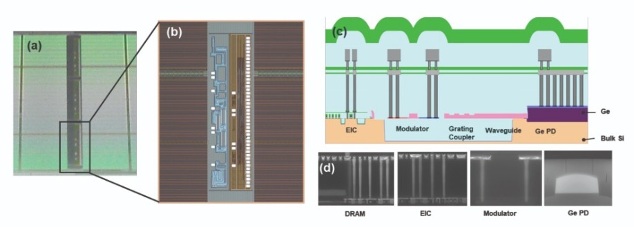
Figure 1. (a) Optical microscope image of a DRAM periphery section. (b) Optical microscope image of the electric-photonic IC. (c) Schematic of the electric-photonic IC vertical structure. (d) Scanning electron microscopy images of the DRAM, electric IC, modulator, and germanium photodiode. Note that this approach, outlined by Samsung in 2013, did not include the integration of lasers.
For this reason, at Samsung Advanced Institute of Technology, we are pursuing photonic IC technology on bulk silicon. Our breakthrough is the development of integrated lasers, implemented with a direct bonding process on the bulk-silicon platform. Our success provides a small but significant step towards the integration of photonic functions into legacy high-volume products, and it could contribute to mainstream semiconductor product evolution.
It makes sense for some smaller companies to develop their photonic technology on SOI, because the size of the emerging market for their technology is large enough for them. But for those of us that are players in the major semiconductor industry, which is already mass-producing electric IC products, the focus tends to be on the electric-photonic ICs. It is this technology that could support the electrical IC market of the future (see Figure 2).
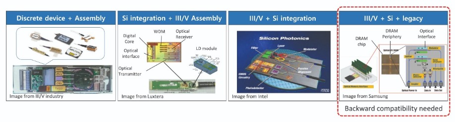
Figure 2. The photonics industry is pursuing several different approaches to unite III-V and silicon technologies. For the last stage of the integration with legacy technologies, photonics integration needs backward compatibility with the legacy platform.
On the bulk silicon platform, developing the integrated laser is the biggest challenge. This building block, like all photonic devices on bulk silicon, suffers from a relatively high optical loss compared with the SOI platform. However, bulk silicon also has its upsides, including a lower cost and a superior heat dissipation that improves laser performance. It is these merits that give the implementation of electric-photonic ICs so much promise.
SOI versus bulk silicon
Despite a cost that is an order of magnitude higher than that of bulk silicon, SOI substrates are firmly established as the mainstream platform for silicon photonics, due to their ease of fabrication, and the low optical loss of the optical waveguides. At the heart of this technology is a global intermediary layer called a buried oxide. It sits beneath the thin crystalline silicon layer, where it creates a low-loss optical waveguide, by surrounding the high-index crystalline silicon core with a low-index oxide cladding. The downside of this architecture, as mentioned before, is its heat dissipation – the thermal conductivity is two orders of magnitude lower than that of silicon.
As this bulk-silicon platform is far lower in cost, and is currently used in most high-volume IC products, it is likely to be used in future electric-photonic ICs. With this platform, it is possible to add a buried oxide locally, under just the optical waveguide. This can impede light leakage, as well as increasing heat dissipation to the substrate, a move that prevents a plummet in the performance of temperature-sensitive devices.
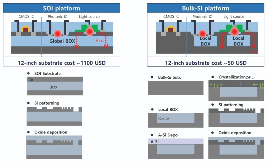
Figure 3. Despite its high-cost substrate, the SOI platform has been dominant in the photonics industry. Merits of the bulk-silicon platform include its low-cost substrate, and its attractiveness for forming electric-photonic ICs. A noteworthy difference between the two architectures is that the SOI platform features a global buried oxide (BOX), while the bulk-silicon platform employs a local BOX.
Integrating III-Vs with silicon
As silicon lasers are still in their infancy, the lasers that are deployed in silicon photonics have to be made from III-Vs. The goal is to ensure low-cost coupling between the III-V laser and the silicon chip. Many solutions have been proposed, ranging from packaging-level assembly to process-level integration. With the assembly approach, the challenge is to realise high-precision optical alignment at low cost, while integration is held back by the substantial investment required to set up integrated processes for handling heterogeneous materials.
Once again, the approach that is adopted is dictated by the size of the industry. If it is small, the preference is on assembly, which provides a swift response to the emerging market; but if a company is operating in the major semiconductor industry, its interest lies in integration, with greater focus on high-volume manufacturing. Turning to integration avoids unacceptable increases in packaging costs, which are forbidden in the major semiconductor industry.
The bonding process is a popular short-term approach to integrating III-Vs and silicon. It overcomes the difference in the lattice constants of heterogeneous materials. Epitaxial layers of III-Vs are grown on a native substrate, before this epiwafer is flip-chip bonded to a silicon substrate that features pre-patterned silicon photonics structures. After the bond has been strengthened with a heat and pressure process, integrated lasers are formed using photolithography and III-V processing. The accuracy provided by lithography eliminates additional alignment.
Unfortunately, the scale and the maturity of silicon and III-V processes are very different. Consequently, integrating them is hampered by various technical and business issues, which may only be addressed with engagement of the overall semiconductor industry.
When pursuing this approach to integration, the first hurdle is to develop a good enough bonding process. Options include buffered bonding and direct bonding (see Figure 4). The former has fewer challenges, but the later delivers a simple silicon-to-III-V connection with diminished wavelength dependency.
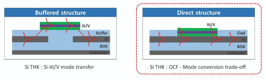
Figure 4. The two main options for bonding are buffered bonding and direct bonding. The buffered structure takes full advantage of the traditional III-V active design and focuses on the smooth laser-waveguide mode transfer. The direct structure relies on an active design that depends on the III-Vs and silicon, and is capable of realising smooth laser-waveguide mode conversion. The thickness of the silicon plays an important role in mode transfer or mode conversion.
Building lasers on bulk silicon
With the bulk-silicon platform, a crystallized silicon layer must be formed on top of the local buried oxide. We do this with our proprietary solid phase epitaxy process. Essentially, this is a form of mild thermal annealing that turns amorphous silicon to crystalized silicon that mirrors the crystalline seed of the substrate. The crystallinity of the substrate propagates upwards in the regions directly contacting the amorphous layer, and propagates sideways over the local buried oxide.
Note that for the silicon at the centre of the local buried oxide, crystallization propagates from both sides – and when they collide, the result is poor crystallinity, known as coalescence. To prevent this poor crystal quality from impairing the performance of the optical waveguide, its location deliberately avoids the coalescence regions.
Putting aside for one moment the use of a local buried oxide and the offset location of the optical waveguide, we employ a process and structure that are similar to the SOI platform. However, our approach offers some advantages over this in terms of flexibility, as we can use arbitrary thicknesses for the silicon layers, the buried oxide, and the polysilicon reflective layers.
The most common method for getting the output of a discrete laser into a waveguide is butt-coupling. This is accomplished by aligning the laser and the waveguide on the same optical axis. In this configuration, the optical mode is positioned at the centre of the laser active region to maximise efficiency.
In this regard integrated lasers are very different, due to the evanescent coupling. The III-V active region is attached to the top of the silicon waveguide, allowing the evanescent tail of this device’s emission to couple with this waveguide. Due to this unique feature, the optical mode is not at the centre of the integrated laser, but distributed over both the III-V and the silicon structures.
With this design, the silicon waveguide provides a resonating cavity structures to the optical mode, and the III-V active region provides optical gain to the optical mode. It is this interplay of the gain and cavity, and how the optical mode is distributed over the silicon and III-V regions, that governs the performance of the integrated laser. For example, if the optical mode is primarily in silicon, this trims the internal loss, cavity loss, and laser-waveguide coupling loss, but at the expense of a reduction in optical gain from the III-V active region. Since the ratio of the optical mode in the III-Vs to that in silicon is determined by the waveguide dimensions, as well as the structure and the thickness of the III-V region, laser development cannot ignore the interplay of the silicon and III-V structures.
Like III-V discrete lasers, if integrated lasers are to work well, the electrical currents must be concentrated in the optical mode. To do this, we use a proton implant process to make the III-V mesa edges non-conductive (see Figure 5). The proton-implanted regions actually serve two purposes: they act as a funnel for current concentration, and they aid the transfer of heat from the active region to the silicon layer. Current is vertically injected into the optical mode from the p-type electrode that sits on top of the III-V mesa, and then it flows in the horizontal direction to drain into the n-type electrode.
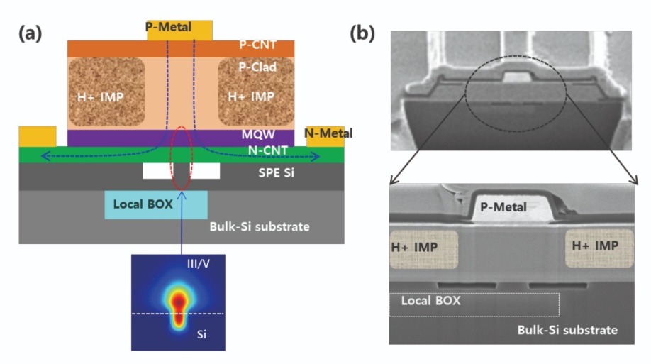
Figure 5. The integrated laser on the bulk-silicon platform includes: a III-V epitaxial layer directly bonded to the pre-patterned silicon wafer; current confinement, realised with the proton-implanted III-V mesa structure; and optical confinement, resulting from the III-V mesa on top of the silicon rib waveguide. Note that to minimise optical loss, there is the lateral offset between the local buried oxide (BOX) structure and the rib waveguide.
Tuning the wavelength?
Depending on the application, the photonic IC may require a laser that emits a single-wavelength or one with a tuneable output. This difference lies in the cavity structure in the silicon side of the integrated laser.
For single-wavelength lasers, the most popular design is the distributed feedback laser (see Figure 6 (a)). By forming a cavity at a single wavelength through a specific grating structure, emission is restricted to a single mode, regardless of driving conditions.
The key metrics for the single-wavelength laser are the wall plug efficiency and the side-mode suppression ratio, which is a measure of the dominance of the lasing mode. In a typical III-V laser, the wall plug efficiency falls as the temperature of the device increases, due to reductions in the gain and the bandgap of the III-V material. In the integrated laser, the situation is more complicated. The thermal behaviour of the silicon must also be considered, and whether its pairing with the III-Vs can apply the brakes to the reduction in wall-plug efficiency with temperature. We have strived to improve the performance of our integrated lasers. This has led us to realise a single-port wall-plug efficiency of 8 percent up to 70 °C and a side-mode suppression ratio of 45 dB (see Figures 6 (c) and (d)).
Several designs are capable of producing a wavelength-tuneable laser. Our device is based on a popular design that features two ring-based mirrors (see Figure 6 (e)). The range of tuning can be broadened with laser mode hopping through the Vernier effect.
With this class of laser, the range of tuning is paramount. Using a proper ring design, we have produced a tuning range of 42.2 nm on the bulk-silicon platform (see Figure 6 (g) and (h)).
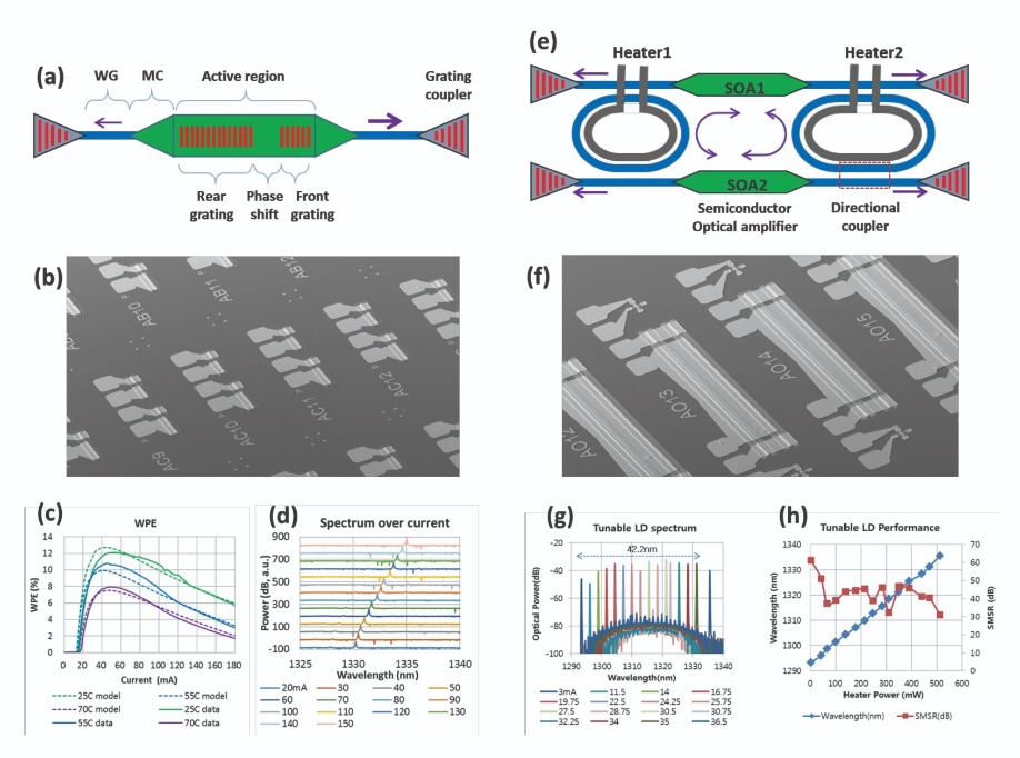
Figure 6. Engineers at Samsung Advanced Institute of Technology have used a bulk-silicon platform to produce and evaluate single-wavelength integrated lasers (see (a) to (d)), and wavelength-tuneable integrated lasers (see (e) to (h)). The single-wavelength laser is a distributed feedback design that realises a high side-mode suppression ratio, and features a quarter-wavelength phase-shift section in the distributed feedback grating (a). Note that this short phase-shift hampers a high wall-plug efficiency, but guarantees single-mode stability. In the integrated lasers, thanks to fine tuning of the design and high precision of the silicon process, it is possible to suppress the deterioration of the mode stability in a longer phase-shift design. To enhance the main-port optical output, the design incorporates an asymmetric cavity structure with different grating lengths on both sides of the phase shift. The wavelength-tuneable laser features a ring-based mirror, with the ring resonator inserted between the two straight waveguides (e). With an optical input to one waveguide, the other waveguide outputs the so-called wavelength comb according to the input wavelength. The result is a mirror-like operation at the selected resonant wavelengths. Note that the ring size determines the wavelength comb periodicity. So, with two rings of different sizes, each ring mirror reflects only at the wavelength comb of a different periodicity. This means that the laser cavity is formed only at the wavelength where the two wavelength combs overlap. If one wavelength comb is then spectrally shifted by the embedded heater of the ring, this action will shift lasing to the adjacent mode in the wavelength comb. (b) and (f) are scanning electron microscopy images of the single-wavelength and tuneable integrated lasers, respectively. (c) Wall-plug efficiency of the single-wavelength laser at 25°C, 55°C, and 75°C. The continuous lines are measurements, and the dotted lines are from a laser model. (d) Optical spectra of the single-wavelength laser, driven at operating currents from 20 mA to 150 mA. (g) Optical spectra of the wavelength-tuneable laser, for a range of heater currents. (h) Lasing wavelength and side-mode suppression ratio extracted from the optical spectra.
We have evaluated the thermal advantage of our bulk-silicon platform by measuring the thermal impedance of our single-wavelength integrated laser. The thermal impedance is defined by the ratio of the temperature change of the laser’s active region, relative to its input electrical power. The greater the heat dissipation, the smaller the impedance. We have found that moving from an SOI integrated laser to one that is on bulk silicon cuts thermal impedance by about 40 percent, assuming no change in the length of the device.
To evaluate the impact of this improvement in thermal impedance on laser performance, we have turned to a measurement-calibrated theoretical model. Based on this insight, at 70 °C we predict that compared to the SOI platform, the use of bulk-silicon enables a 52 percent hike in the maximum optical output power and a 13 percent increase in the wall plug efficiency (see Figure 7). And if we were to thin the substrate, the resulting reduction in thermal impedance could increase the maximum optical output power at 70 °C by more than 140 percent. Based on this modelling, the bulk-silicon platform is particularly promising for electric-photonic ICs that require either many temperature-sensitive devices or high-power lasers.
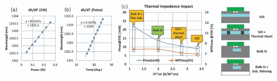
Figure 7. Thermal analyses of the single-wavelength laser on the bulk-silicon platform. It is challenging to undertake direct measurements of local temperature change in the active region, so this characteristic is indirectly measured through lasing wavelength change. Rates of lasing wavelength change are measured in terms of temperature and input power, with the ratio of these two revealing the thermal impedance. (a) Lasing wavelength shift over increasing power in continuous operation. (b) Lasing wavelength shift over increasing temperature, using pulsed excitation with a 0.1 percent duty cycle. (c) The maximum output power and the maximum wall-plug efficiency at 70 °C, calculated using the laser model for the four platforms of interest. The calculation is calibrated with the measured data of the bulk-silicon platform.
Figure 8. (a) A high-temperature operating lifetime test, conducted at 70°C, run over 1900 hours with 24 single-wavelength lasers. The output power was set to 6 mW. (b) The cumulative failure plot provides an estimate for device lifetime.
Dongjae Shin et al. “Heterogeneously integrated light sources for bulk-silicon platform,” IEDM2018, 23.6 2018
Dongjae Shin et al. “Integration of silicon photonics into DRAM process,” OFC 2013, OTu2C 2013
Spurring the development of silicon photonics is the world’s first InP-based laser grown on exactly orientated silicon
BY KEI MAY LAU AND YU HAN FROM HONG KONG UNIVERSITY OF SCIENCE AND TECHNOLOGY
We are living in a zettabyte era, where digital data is generated, processed, stored, and transmitted at unprecedented rates. Demand for data is only going to increase, and satisfying this will not be easy. However, it can be fulfilled by silicon photonics, drawing on cost-effective microelectronics technologies to realize ultra-high-bandwidth, power-efficient photonics on the traditional silicon platform.
An essential but elusive component for silicon photonics is a compact, efficient, on-chip semiconductor light source. For the past decade, the development of this source has focused on heterogeneous integration – that is, the bonding of conventional III-V semiconductor laser dies onto silicon photonic wafers. This hybrid integration technique is not as attractive as monolithic integration, involving the direct growth of III-V lasers on silicon. But realising the latter is more challenging, partly because in order to ensure compatibility with present IC technology, lasers must be integrated on CMOS-standard (001)-oriented silicon substrates without an offcut. The offcut (mis-orientation) was deemed necessary to overcome the anti-phase boundary defects formed when growing polar semiconductors (III-V) on non-polar silicon. What’s more, as the ICs will be used in data communications, these lasers must operate at telecommunication wavelengths – the 1.3 µm and 1.5 µm band. And if this approach is to be commercially successful, the lasers that are produced must deliver a high performance, and be coupled with other silicon photonics components in a scalable, cost-effective manner.
At Hong Kong University of Science and Technology, we can address most of these concerns with a technology that enables direct hetero-epitaxy of III-V coherent lasers on silicon substrates. This approach, involving MOCVD, offers the potential for lower cost, higher yield, and scalability than chip-scale bonding.
One of the challenges of direct growth is how to address the polarity and lattice mismatch between the III-Vs and silicon. Crystalline defects emerge from the III-V/silicon interface, including various kinds of dislocations, and they can jeopardize laser performance and reliability. Special techniques are required to suppress the generation and propagation of these dislocations, and enable efficient light emission on silicon substrates. We are pioneering one promising solution, based on low dimensional In(Ga)As quantum structures. By embedding quantum dots inside optimized InP buffer layers that are grown on silicon substrates, we are able to use MOCVD to produce 1.5 µm-band InP-based lasers on industry-standard silicon wafers.
Quantum dot lasers on silicon
Fabrication of our lasers begins with the growth of III-V alloys on 300 mm nano-patterned silicon wafers. This involves a unique patterned growth process on exact (001)-oriented silicon substrates, rather than 2-6° offcut silicon, the platform adopted by many other groups (see Figure 1(a)). Our efforts begin by creating [110]-aligned oxide trenches atop the silicon wafer. Anisotropic wet etching follows, to obtain densely packed V-shaped pockets with two concave, atomic-sharp {111} surfaces. By nucleating GaAs inside these nano-pockets, we eliminate the formation of anti-phase boundaries – a crystalline defects that is detrimental to devices. We find that GaAs nanowires first nucleate inside the nano-pockets that coat the {111} surfaces. Continued growth leads to the coalescence, creating thin films. Thanks to the unique tiara-shape of the nano-pockets, we find that the planar defects generated at the interface of GaAs and silicon are unable to propagate into the above heterostructures (see Figure 1(c)).
Our next step is to grow an InP layer on the coalesced thin film of GaAs. Due to the 4 percent lattice mismatch between InP and GaAs, dislocations appear at the interface between these two materials. To prevent them from propagating into device regions, we insert ten periods of In0.6Ga0.4As/ InP strain layer superlattices inside the InP buffer. The strain inside these superlattices changes the propagation direction of the dislocations, causing them to either annihilate or propagate to the edge of the sample (see Figure 1(b)).
We have scrutinised the quality of our material with transmission electron microscopy. This reveals a defect density of 1.5×108 cm-2, which is one of the lowest values reported for an InP thin film grown on silicon (see Figure 1(d)). We believe this is not the limit, and are currently exploring new methods to further reduce the defect density.
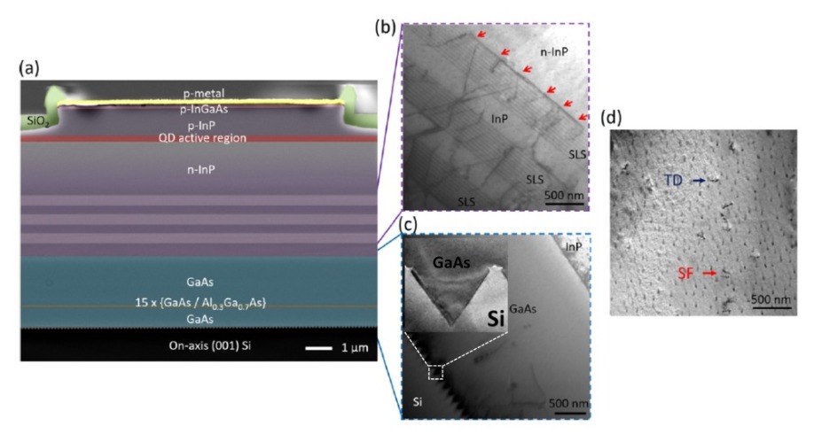
Figure 1. (a) Colour-enhanced cross-sectional scanning electron microscopy image of the whole epitaxial structure after laser fabrication. (b) Cross-sectional transmission electron microscopy images of three stacks of a 10-period InGaAs/InP strain-layer superlattices with dislocation filtering effects identified by red arrows, (c) 2.2 µm-thick GaAs intermediate buffer on a nano-patterned V-grooved on-axis (001) silicon substrate; inset shows the defect trapping effect of the tiara-shaped pocket enclosed by {111} facets. (d) Plan-view transmission electron microscopy characterization of defect density of the InP buffer on silicon.
To see if they can fulfil their promise, we have embedded five layers of InAs quantum dots inside a laser structure on the InP buffer. Each of the layers of dots, formed using the Stanski-Krastanow growth mode, is capped with two layers of optimised InAlGaAs spacers. They have a thickness that has been carefully tuned to ensure a strong, narrow photoluminescence spectra.
Atomic force microscopy reveals that our samples have a quantum dot density of 4.5 × 1010 cm-2 (see Figure 2 (a)). This technique has also evaluated the flatness of the surface of the full laser structure. It has a surface roughness of just 1.4 nm (Fig. 2(b)). Meanwhile, photoluminescence measurements produce a strong peak centred at the 1.5 µm band (see Figure 2(a)).
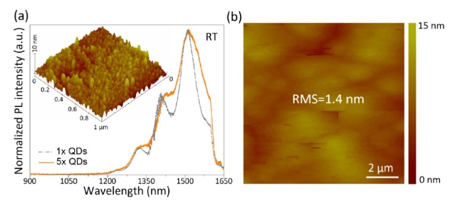
Figure 2. (a) Normalized room-temperature photoluminescence spectra of 1 and 5 layers of quantum dot active regions grown on silicon. Inset shows an atomic force microscopy image of the top layer quantum dots with a dot density of 4.5 × 1010 cm-2. (b) Atomic force microscopy image of the as-grown quantum dot laser on silicon, showing a smooth surface with a root-mean-square value of 1.4 nm.
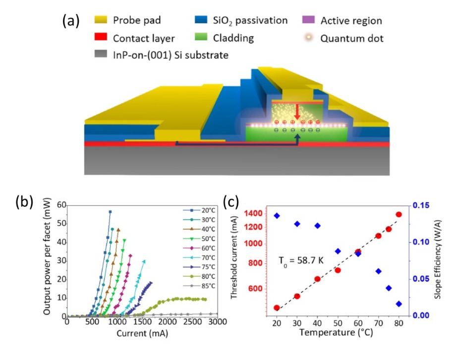
Figure 3. (a) Schematic of an InAs/InAlGaAs/InP quantum dot laser on silicon substrates. (b) Light output power versus current for a 20 µm × 1000 µm device at various temperatures. (c) Threshold current and slope efficiency change as a function of temperature. The characteristic temperature is extracted to be 58.7 K.
This result is an important step towards our goal of equipping silicon photonic chips with efficient light emitters, in the form of high-performance 1.5 µm quantum dot lasers directly grown on silicon. Right now, we are targeting continuous-wave operation, a goal that we hope to accomplish by reducing the dislocation density of the InP-on-silicon template, improving the quantum efficiency of InAs quantum dots, and optimising the overall laser structure.
Lasers at the nano-scale
Our efforts have also focused on the direct epitaxy of 1.5 µm InP-based nano-lasers on silicon substrates. Like the scaling of silicon transistors, as governed by Moore’s Law, the shrinking of the laser footprint to nanometre scale delivers several benefits. In this case it cuts energy consumption, while increasing the integration density of silicon photonic integrated circuits.
The starting point for the creation of our nano-lasers, featuring InP nano-ridges, is nano-patterned, (001)-oriented, silicon-on-insulator (SOI) substrates. Using the aspect ratio trapping technique, we begin by depositing an ultra-thin GaAs wetting layer – it is around 10 nm-thick – at the {111} silicon surface, to facilitate subsequent InP nucleation. With this approach we can confine most of the crystalline defects within the III-V/silicon interface, due to the unique strain-relaxing mechanism (see Figure 4(b)).
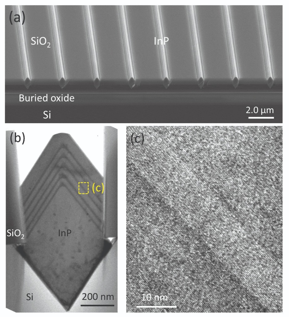
Figure 4. (a) Scanning electron microscopy image of the highly ordered, in-plane InP/InGaAs nano-ridge structures on (001) silicon-on-insulator wafers. (b) Cross-sectional transmission electron microscopy image of the InP/InGaAs nano-ridge perpendicular to the wire, showing five {111} ridge InGaAs quantum wells embedded inside an InP nano-ridge; the dark area at the InP/silicon interface contains a high density of stacking faults generated for strain relaxation. (c) High-resolution transmission electron microscopy image of one InGaAs ridge quantum well with atomic sharp InP/InGaAs interfaces.
Our solution is cycled growth. This allows us to manipulate the distribution of InGaAs on the multi-faceted InP ridge buffer at a single-atomic-layer level. As a result, we can grow InGaAs quantum wells with atomic sharp interfaces and superior optical properties (see Figure 4(c)).
One of the key challenges with nano-lasers on silicon is the confinement of the optical modes within the sub-wavelength nano-cavities. We improve the confinement with a hybrid InP/InGaAs Fabry-Pérot nano-cavity design that is supported by silicon pedestals (see Figure 5(a)). The silicon pedestal is formed via anisotropic wet etching, with the dimensions carefully controlled to ensure both strong optical confinement inside the nano-ridge and robust mechanical support for the top laser cavity (see
Figure 5 (b) and 5 (c)). The silicon pedestal, which features atomically sharp {111} surfaces, could also serve as a low-loss waveguide. This structure could couple light from the laser cavity above, providing potential on-chip light manipulation.
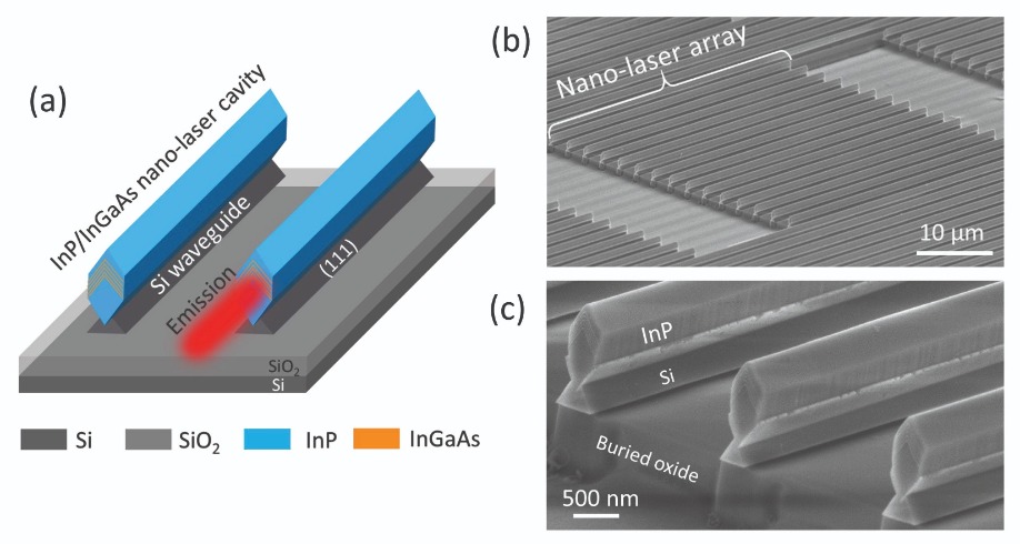
Figure 5. (a) Schematic of the designed InP/InGaAs nano-laser array grown on an SOI substrate. (b) Tilted-view scanning electron microscopy image of the InP/InGaAs nano-laser array on SOI. (c) Zoomed-in scanning electron microscopy image of the end-facets of the nano-laser array.
Optical pumping
Measurements on our laser with a 60 µm cavity reveal that optical pumping produces room-temperature lasing in the 1.5 µm band. Under low excitation, the output from the nano-laser combines broad spontaneous emission with well-spaced Fabry-Pérot resonance peaks. Crank up the pumping, and a 1518 nm peak protrudes from the background emission, before lasing kicks in. Far above threshold, the intensity of the 1518 nm single-lasing-mode is orders of magnitude higher than the clamped background emission. Further support for lasing is the apparent threshold behaviour in the plot of output with pump power, and the line-width narrowing of the emission peak (see Figure 6(b)).
Figure 6. (a) Room-temperature emission spectra around threshold. Inset shows the emission spectra plotted in a logarithmic scale. (b) The evolution of the peak intensity and the line-width as the excitation level increases. Inset presents the progression of peak position as a function of pumping levels. (c) The relationship of the lasing peak and the length of the nano-cavity.
This correlation between the lasing mode and the cavity length stems from the wavelength-dependent modal gain and propagation/end-facet loss. As a longer wavelength leads to a larger round-trip loss and a smaller modal gain, a larger volume of active material is needed to reach threshold. The opportunity to tune the lasing wavelength over multiple telecom bands suggests that our technology could serve in compact wavelength-division multiplexing systems.
Our incorporation of a telecom nano-laser array onto CMOS-compatible, (001)-oriented SOI substrates highlights the feasibility of on-chip integration between compact III-V nano-scale light sources and mature silicon photonic components. Aiming at developing nano-scale photonic integrated circuits on SOI, we are now focusing on the design of electrically driven nano-lasers on SOI wafers. Look out for our future publications, as we are confident that we will soon have more promising results to report.
Q. Li et al. Appl. Phys. Lett. 106 072105 (2015)
S. Zhu et al. Appl. Phys. Lett. 113 221103 (2018)
Y. Han et al. Appl. Phys. Lett. 108 242105 (2016)
Y. Han et al. Optics Letters. 44 767 (2019)
The Fraunhofer Heinrich Hertz Institut (HHI) is at the forefront of optochip and photonic integrated circuit (PIC) research. Executive Director Martin Schell provides insight into the Institut’s latest work with EMLs, EAMs and Mach-Zender modulators between 25 and 100 GBit/sec.
“Annual global IP traffic will reach 3.3 Zbyte per year by 2021…..” This forecast recently published by Cisco [1] looks like a huge market for transmitters, and receivers alike. On a closer inspection, however, optical component makers may get less excited. Thanks (or owing) to fantastic achievements on the high-speed performance of key components in recent years, single transmitter devices of fairly manageable design are capable today of delivering a modulation rate on the order of 50 Gb/s -100 Gb/s, and even beyond that when using more complex configurations.
Much of the IP traffic ends in data centers. Their typical architecture requires top-layer intra-center optical connections of 500 m to 2 km distance, and of up to 40-80 km between such facilities. Single-mode operation is of course compelling here. A simple calculation reveals that supporting a yearly data volume of 3.3 Zbyte, equivalent to an average data rate of about 8.3x1014 bit/s, would – theoretically – only need some 16,000 pieces of 50 Gb/s transmitter chips. With electro-absorption modulated lasers (EML), outlined below, these could be accommodated on a single wafer of 3-inch diameter, today’s standard size in InP technology.
In the end, the situation will not be as bad like that: One north-south bit may cause hundreds of east-west bits; the same bit may pass a couple of transmitters; and data centers should be equipped to handle peak traffic. A recent analysis of AIM Photonics Academy [2] concludes that for the data centers operated by the four giants: Amazon, Facebook, Google, and Microsoft, there will be a demand of approximately 22m pieces of 100 Gb/s transceivers per annum, translating into a lower 4-digit 3” wafer quantity. With 8 wafers grown in a single run, this would correspond to about 150 of 4-hour epitaxy runs per year for the base wafer.
Silicon Photonics (SiP) is being widely regarded as the technology of choice for implementing intra-datacenter transceivers using electro-optic modulators for data generation. Despite tremendous progress made during the past years, SiP is lacking the ability to make practical Si-based lasers, and in fact there is no solution in sight. Consequently, InP-based source lasers have to be incorporated, either by demanding hybrid assembly techniques or by a hetero-integration (e.g. wafer bonding) approach. While the former represents a serial manufacturing process the latter requires additional on-wafer InP processing which questions the economic advantages of the Si core technology. InP technology, on the other hand, provides the only material platform enabling true monolithic laser integration. This enables extremely efficient and small-footprint ultrahigh-bitrate transmitter chips. Whereas directly modulated DFB laser devices may be useful up to 25 Gb/s, EML structures are predestined for achieving much higher modulation rates and concomitantly higher transmission distances, thanks to the adjustability of zero and even negative modulation chirp.
Fraunhofer HHI has been pursuing an intense program to develop EMLs over almost a decade. A fairly simple design has been adopted that uses an identical layer structure for both the DFB source laser and the electro-absorption modulator (EAM). The active region consists of InGaAlAs quantum well layers. With etching an isolation trench between the DFB and the EAM section as a key manufacturing step on top of standard lasers, EMLs now have developed into reliable high-yield devices [3].
Typical performance parameters of HHI’s EML devices, featuring a 300 µm long DFB laser and an 80…120 µm long EAM section, are characterized by a static extinction ratio of > 20 dB at an EAM voltage swing of 2 V. A typical bias voltage is about -1 V, and below this point the chirp factor tends to become zero, and even negative when further shifting the bias towards larger negative values. The optical output power reaches some 5 dBm, generally limited by the fact that the DFB laser is not operated at optimum gain but is detuned to longer wavelengths to guarantee transparency of the electro-absorption modulator in the on-state.
To overcome that design-inherent issue, an optical booster amplifier has been added (Fig. 1) which provides output powers of >10 dBm. Even at 56 Gb/s the integrated amplifier does not affect the modulation behavior [4].
Figure 1: Top view of HHI’s EML chip comprising an optical amplifier (OA) section to boost the output power. All of the three sections (DFB, EAM, OA) are made of the same layer structure, with electrical separation between them achieved by isolation trenches. The optical output is tilted to help suppress optical back-reflection. RF feeding of the EAM part is supported by a Ground-Signal-Ground (GSG) transmission line.
Thanks to this upgrade, next-generation PON requirements (average modulated output power of min 9 dBm @10 Gb/s; 1577 nm) can readily be met. The modulation rate of 56 GBd is routinely achievable now. However, a baud rate of 100 GBd has been demonstrated very recently (Fig. 2) after introducing further design refinements.
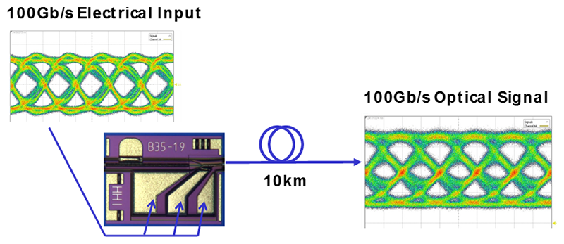
Figure 2: Demonstration of 100 Gb/s EML modulation capability (NRZ; λ=1300 nm; chip size: 420 µm x 320 µm)
Hence, a single-wavelength 100 G transmitter (on-off keying) may be implemented using a single tiny EML chip, provided suitable electrical drivers are available. In addition or instead, however, virtually all the common multiplex methods are applicable to efficiently accomplish even higher data rates and/or to exploit lower baud rates. 4- and 8-level Pulsed Amplitude Modulation (PAM) was successfully demonstrated on HHI’s EMLs. Using a proprietary SiGe based driver IC, clear 32 GBd PAM4 eye diagrams have been achieved at a driver power of 84 mW leading to a figure-of-merit of 1.3 pJ/bit (Fig. 3).
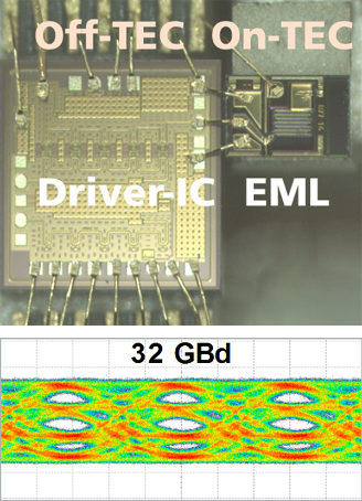
Figure 3: EML chip with co-packaged PAM4 driver IC designed at HHI. Power consumption of the driver IC is 84 mW (top); PAM4 eye diagram received at 32 GBd (bottom)
For space-division-multiplexed transmission, a serial dual-EML chip has been designed that comprises two EAMs in back-to-back configuration sharing the same DFB source laser between them [5]. Simultaneous modulation without mutual interference was demonstrated at 56 GBd (Fig. 4).
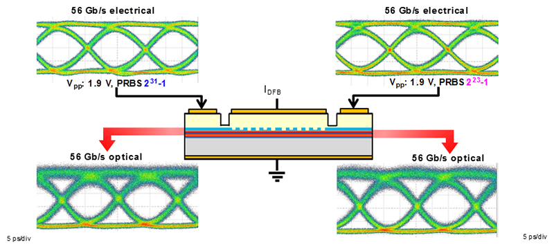
Figure 4: Dual-EML device sharing a common DFB source laser
For PAM4 schemes, a parallel 4-EML array was fabricated [6] which is capable of delivering an aggregated data rate of 224 Gb/s (4x 56 GBd). As a special feature, in this array the RF connections to the EAMs have been routed to the rear edge of the chip thus providing uniform RF driving conditions and concurrently facilitating packaging. While EMLs are now commonly used under TEC controlled conditions, typically at 40-50°C heat-sink temperature, uncooled operation (xx-90°) has been demonstrated recently.
Finally, generation of polarization-multiplexed signals has been shown. To this end, a photonic integrated circuit combines two EAM elements serially integrated with combiner/splitter-free polarization converters [7] and a DFB laser, as sketched in Fig. 5.
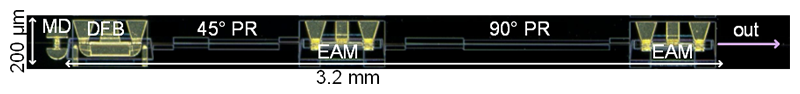
Figure 5: Image of a fabricated integrated Dual-Polarization EML device, consisting of (from left to right): a monitor photodiode (MD), a DFB laser diode emitting TE polarized light, two polarization converters, and two EAMs. The first polarization converter (45° PR) rotates the polarization by 45°, and the first EAM modulates the 50% of the laser light that remains TE-polarized. The following converter (90° PR) rotates the signal by 90° thus interchanging the TE and TM fractions. The second EAM modulates the light that was previously not modulated by the first EAM. The device was realized on HHI’s PIC foundry platform.
Respective chips have been fabricated on HHI’s generic PIC platform [8], and its functionality was successfully tested at 20 Gb/s per polarization state [9]. Such a chip measures only 3.2 mm x 0.2 mm. On a precursor chip without integrated laser, a total bit rate of 112 Gb/s was obtained using a baud rate of 28 GBd and PAM4 modulation [10]. By further inserting a phase shifter to modulate the optical phase between the TE- and TM-signal, a very compact transmitter for true 3-dimensional Stokes-vector modulation (SVM) could easily be implemented, delivering a bit rate corresponding to the threefold baud rate, and sixfold if additionally applying PAM4 signaling to each of the three channels. SVM represents a promising new direct modulate-and-detect technique, with a complexity and performance somewhere between direct and coherent transmission. This may have high potential for 100G access and metro networks –to make room for some more zettabytes to come.
An alternative to electro-absorption modulators is the Mach-Zehnder modulator (MZM). MZMs exploit the quantum–confined Stark effect which is quite efficient in InP based materials, particularly when using MQW structures. In comparison to EAMs, MZM devices build much longer (4… 8 mm). This is rewarded by higher static extinction ratios (> 25 dB), operation over a wider wavelength span (~ 50 nm), and eventually probably higher electro-optic bandwidth.
As with EMLs, there is long-standing experience and expertise with Mach-Zehnder modulators on InP at Fraunhofer HHI. Already in an early development stage, a traveling-wave electrode design has been introduced to boost the bandwidth. Meanwhile, a wide range of discrete as well as integrated modulator structures of high complexity (e. g. IQ modulators) have been developed. Some of them have been transferred into commercial products by partnering with companies. Among the more recent developments is an O-band MZM that has been monolithically integrated with a DFB laser. A key step further was the co-design of the electrical driver aimed at lowest power consumption. To this end, a 2-bit digital-to-analog converter was designed for optimum impedance matching. ICs were fabricated on a 0.13 µm SiGe BiCMOS foundry platform. Fig. 6 shows a transmitter subassembly combining this IC and the DFB-MZM PIC. Tested at 56 GBd, PAM4 modulation the overall power consumption including the laser, the modulator and the driver amounted to only 332 mW [11].
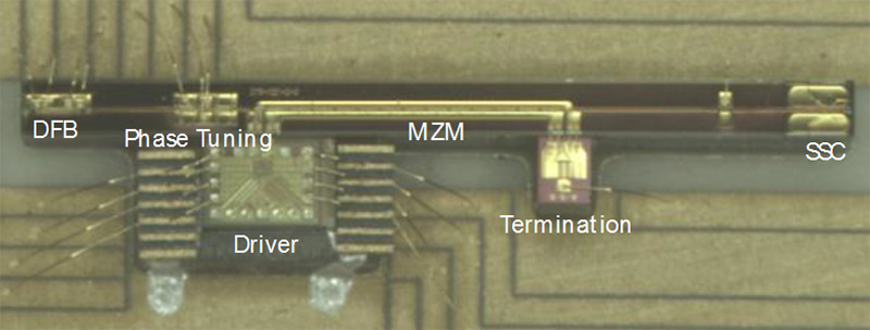
Figure 6: Co-packaged transmitter subassembly comprising the DFB-MZM chip, a 2-bit DAC driver and a load resistor. The unit was successfully tested at 56 GBd, PAM4 modulation requiring a total power consumption of only 332 mW
[1] Cisco White Paper” The Zettabyte Era: Trends and Analysis”, June 7, 2017
[2] AIM Photonics Academy; “Integrated Photonics Grand Challenges and Key Needs for 2018”, Webinar Dec 21, 2017
[3] M. Moehrle, H. Klein, C. Bornholdt, G. Przyrembel, A. Sigmund, W.-D. Molzow, U. Troppenz and H.-G. Bach, „InGaAlAs RW-based Electro-Absorption-Modulated DFB-Lasers for High Speed Applications”, SPIE Photonics Europe 2014, Brussels, invited paper 9134-44
[4] M. Theurer, G. Przyrembel, A. Sigmund, W. D. Molzow, U. Troppenz, M. Möhrle, „56 Gb/s L-band InGaAlAs ridge waveguide electro-absorption modulated laser with integrated SOA“, Phys. Stat. Sol. A213, 970-974, 2016
[5] M. Theurer, H. Zhang, Y. Wang, W. Chen, L. Zeng, U. Troppenz, G. Przyrembel, A. Sigmund, M. Moehrle, and M. Schell, “2 x 56 GB/s from a Double Side Electroabsorption Modulated DFB Laser and Application in Novel Optical PAM4 Generation”, J. Lightw. Techn., vol. 35, no. 4, pp. 706-710, 2017
[6] M. Theurer, M. Moehrle, U. Troppenz, H.-G. Bach, A. Sigmund, G. Przyrembel, M. Gruner, M. Schell, „4 x 56 Gb/s high output power electroabsorption modulated laser array with up to 7km Fibre Transmission in L-Band”, J. Lightw. Techn., vol. 36, no. 2, pp. 181-186, 2018
[7] M. Baier, F. M. Soares, M. Moehrle, N. Grote, M. Schell, “Highly fabrication tolerant polarization converter for generic photonic integration technology”, 28th IPRM (2016), paper MoC3-6
[8] F. M. Soares et al.,” High-Performance InP PIC Technology Development based on a Generic Photonic Integration Foundry”, OFC 2018, paper M3F.3 See also cover story of PIC Magazine, issue 4 (March 2017): “PICs at Fraunhofer HHI: Adding strength to InP photonic integration “
[9] M. Baier, F. M. Soares, T. Gaertner, A. Schoenau, M. Moehrle, M. Schell, “New Polarization Multiplexed Externally Modulated Laser PIC”, ECOC 2018, paper submitted
[10] M. Baier et al., “112 Gb/s PDM-PAM4 Generation and 80 km Transmission Using a Novel Monolithically Integrated Dual-Polarization Electro-Absorption Modulator InP PIC,” Proc. ECOC 2017, Th.1.C.4
[11] S. Lange et al., “Low Power Optical Transmitter with DFB-Laser Mach-Zehnder Modulator PIC and Co-Designed 2-Bit DAC Driver,” Proc. ECOC 2017, Th.1.C.5
A newly-patented imec concept utilizes silicon photonics and thousands of tiny interferometers to reduce a Raman spectroscope to the size of a smartphone.
By: Els Parton, Harrie Tilmans & Pol Van Dorpe


Raman Spectroscopy is a time-tested means to analyze the composition of materials using a portion of light reflected from a sample into the instrument. Today’s most commonly available, highly accurate Raman spectroscopes are desktop-sized and expensive; handheld versions suffer from performance limitations and are also costly. Unlike existing handheld spectroscopes, imec’s new concept exhibits the high optical throughput and spectral resolution of a desktop system, opening a whole new range of applications in which complex samples can be analyzed with a more affordable handheld device.
From medieval paintings to drugs
Raman spectroscopy was discovered by C. V. Raman in 1928, which earned him the Nobel Prize for Physics in 1930. Raman spectroscopy is used to identify materials – fluids, powders, solids – and to learn more about the materials composition. Today’s spectroscopes shine laser light on the material, and by analyzing a specific part of the scattered light, a spectral chart can be made. The scattered light that is analyzed is the so-called ‘Raman scatter,’ which is characterized by a different wavelength than the laser’s wavelength. It originates from the molecular vibrations in the material. One can recognize the spectral ‘fingerprint’ of each material and compound in the spectral chart.
Raman spectroscopy is used in many different fields – in fact, it can be used in any application where non-destructive material analysis is needed. For example: in pharmaceutics, Raman discloses the distribution of active compounds in medicinal tablets. Raman can also classify meteorites in chondrites and achondrites based on its mineral composition. It can even dive into the kind of hybridization in a (carbon) molecule and tell whether it’s a sp2 or sp3 hybridization. In semiconductor R&D, Raman spectroscopy can be used to determine the electrical properties and the number of layers of graphene, or characterize the stress in specific layers. In life sciences, Raman is able to tell something about the interaction between cells and specific drugs. In art work, the technique is used to identify which pigments were used, which in turn can give an indication about the artist’s identity, his working method, and the age of the work. Even the mummified skin of ‘Otzi the Alpine Iceman’ was examined with Raman spectroscopy.
Existing devices: desktop and handheld
Numerous Raman spectroscopes are available today, specifically tuned to varied applications. Raman systems are often implemented as a microscope where the sample is illuminated with a diffraction limited spot and the Raman photons are collected with a high NA (numerical aperture) objective. Next to these desktop devices (which make up the largest part of the market), handheld counterparts have also emerged. These are really convenient for research ‘in the field’ like in the case of art work studies or archeology.
As is often the case with miniaturized versions of measuring equipment, handheld Raman spectroscopes are not as good as the desktop versions. For the study of the pigments in paintings, they work fine because the pigments generate strong Raman signals, but for more complex samples such as opaque fluids (such as milk), skin or powders, the current systems are not adequate or need a long measuring time. Also, the high pricing of handheld Raman spectroscopes inhibits widespread use.
What if a cheap but high performance handheld Raman spectroscope was available? Which new applications would be made possible? Think of food screening ‘on the go,’ skin screening for melanoma at the general practitioner’s office, or screening for drug authenticity by authorities throughout the supply chain. Within the food and beverage industry, it can be used for characterization purposes and for identifying and evaluating the authenticity, safety and quality attributes for a broad range of food and agricultural products. For instance, Raman is an ideal technique to identify and indicate the adulteration of edible oils or to determine the level of alcohol in beverages. Multiple component analysis using Raman spectroscopy is key (for example) in understanding the quality of milk by determining the fat, protein and water content of the milk a cow or a goat is producing (in real time). For cosmetics, Raman spectroscopy can be used for verification of the purity of ingredients such as those used in personalized moisturizing creams and essential oils (eucalyptus, ginger, lavender, basil, vanilla). Furthermore, it can be used to determine the remaining concentration of solvents in pharmaceutical preparations to decide if the level of nutrition is sufficient for a certain cell culture to maintain their growth.
Why is it difficult to further improve current handheld devices?
There are two main challenges in developing Raman systems. First of all, spontaneous Raman scattering is typically very weak, and as a result the main difficulty of Raman spectroscopy is separating the weak inelastically scattered light from the intense Rayleigh scattered laser light.
Secondly, in strongly scattering media, such as food or human tissue, the incident photons are not confined in a small spot, but instead generate a blurred spot, with sizes up to several millimeters. This increases the “optical throughput” or “etendue,” which is a measure for the spread of the light in space and angle. A spectrometer usually limits the etendue, which drops for compact devices.
In commonly used dispersive spectrometers, the light is focused on a slit, and its spectral components are separated using a diffraction grating. Miniaturization of a high spectral resolution device (<1 nm) requires a reduction in the slit width, thus reducing the etendue.
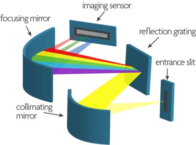
Figure 1: Existing dispersive handheld spectrometers make use of entrance slits, mirrors, and gratings like those indicated in this scheme. In this way, the etendue and spectral resolution are coupled through the size of the entrance slit. Downscaling of the spectrometer leads to lower spectral resolution or acceptance etendue.
Ultimate miniaturization of optical devices can be realized using integrated photonics and waveguides. The etendue of a single-mode waveguide (which is the ultimate scaling of this approach) equals approximately λ², with λ the wavelength. If the used wavelengths is (for example) 860nm, this results in an etendue of 7.3e-7 mm²sr, which is 106-107 times lower than required for analyzing diffuse scattering samples.
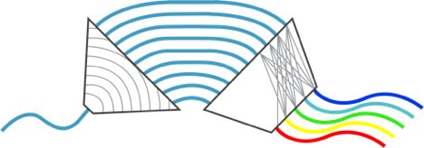
Figure 2: Existing photonic-based handheld spectrometers are limited in miniaturization by the etendue of single-mode waveguides.
A spatially heterodyne spectrometer based on silicon photonics
Because of the limitations of current approaches in handheld Raman spectrometers, other concepts have been investigated. Another class of spectroscopy is based on light interference and implemented (for instance) in Fourier transform spectroscopy or in spatially heterodyne spectroscopy. These concepts exhibit an intrinsically larger etendue and are therefore more ‘scaling proof’.
A well-known Fourier Transform spectrometer is based on the Michelson interferometer. A beam of light is divided into two beams that take different paths before coming together and interfering. This enables tiny differences in the wavelength to be measured. The disadvantage of this design – particularly if you want to miniaturize it – is that two mirrors are used, one of which moves.
Researchers from imec have now developed an integrated photonics version of such a scheme without moving parts: the integrated spatially heterodyne spectrometer. The etendue is less limited in this case and equals n x λ², with n being the number of interferometers. As mentioned above, if the used wavelength is (for example) 860nm, and the preferred etendue (for complex samples) is around 0.5 mm²sr, then about a million interferometers would be needed.
This massive parallelization is possible with integrated photonics. The patented solution monolithically integrates close to a million interferometers on top of CMOS image sensors and light is delivered using micromirrors.
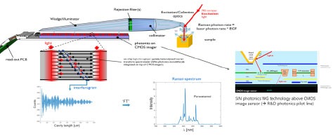
Figure 3: Concept of the patented solution made by imec researchers for a handheld Raman spectrometer, using a million interferometers on top of a CMOS image sensor. This build-up allows for extreme miniaturization without compromising on the etendue of the sample. This way, complex samples can also be measured. Furthermore, by using chip technology, the price of the device can be much lower than current devices.
This is the working principle of the newly developed Raman spectrometer: Laser light (785nm wavelength) is focused on a sample and the scattered photons are collected and collimated by means of a compound parabolic concentrator (CPC). After filtering the Rayleigh photons (at 785nm), Raman photons are directed to the on-chip waveguide (WG) access ports using a wedge-shaped light guide and chip-integrated micromirrors. By a proper choice of the wedge shape and the angle of the incident light, the micromirrors are able to redirect the light with a large efficiency (>50%), where it is coupled into the WGs thru gratings linked to individual single mode WG interferometers. The interferometers exhibit a range of lengths, allowing for reconstruction of the original spectrum. Their outputs are aligned with the pixel pitch of the integrated CMOS image sensor serving as a highly parallelized detector array. The chip is wire-bonded to a PCB and connected to a custom designed read-out board to capture the data and transfer it to a computing device, which reconstructs the spectrum and displays the required property.
Silicon nitride is the material of choice for the waveguides
Due to requirements of CMOS compatibility and visible transparency, silicon nitride was chosen as the waveguide material. The WG stack is built monolithically on top of the BEOL of 200mm front side illuminated CMOS image sensor wafers. Post-processing is done in a 200mm CMOS pilot line, using 193nm DUV lithography for patterning the WGs and grating couplers.
The spectrometer chip is constructed using SiN-based waveguide photonics, implemented on top of a CMOS image sensor (CIS) used for electrical readout. The spectrometer chip as used in the current design consists of an array of massively parallel evanescently-coupled Fabry-Perot interferometers, varying in length in the range 2.2-152.8µm (in linear steps of 0.2µm). Incident light is coupled into the waveguide structures using a grating based in-coupler (GC). Sloped metal output mirrors are used to couple the light from the waveguide to the readout pixels of the CIS (see also insert with a cross-section of the chip in figure above). An illustration of the layout showing a top view of the F-P resonators together with the grating in-coupler and sloped metal output mirror is shown in the figure below.
Figure 4: Part of the spectrometer chip layout, showing an evanescently coupled Fabry-Perot resonator (17.6µm long) together with the grating in-coupler(s) and the sloped output mirror for coupling the light to the pixels.
Conclusions
Raman spectroscopy is a powerful analytical technique with numerous applications. Existing desktop devices are rather bulky and have a price range of a few hundred thousand dollars/euros. The handheld solutions that exist today fail to reach the desired performance for high-end applications. Thanks to a new concept, it is now possible to overcome this performance barrier. By massive parallelization of waveguide interferometers integrated monolithically on top of a CMOS image sensor, both high optical throughput and high spectral resolution can be reached in a miniaturized device. This novel system is built in imec’s SiN biophotonics platform that guarantees robustness and compatibility with high-volume manufacturing.
Acknowledgements
Part of the work was performed under the EU-funded IoSense project; the authors acknowledge the funding received from the Electronic Component Systems for European Leadership Joint Undertaking (ECSEL-JU) under grant agreement No 692480 (Project Acronym: IoSense). This Joint Undertaking receives support from the European Union’s Horizon 2020 research and innovation programme as well as Germany, The Netherlands, Spain, Austria, Belgium, and Slovakia.
About Els Parton
Els Parton received her engineering degree and PhD at the KU Leuven, Belgium. She joined imec in 2001 as a scientific editor. In addition to writing numerous articles on imec research, she is editor-in-chief of imec magazine, a digital magazine published every month. www.imecmagazine.com
About Harrie Tilmans
Harrie Tilmans received his Ph.D. degree in Electrical Engineering from the University of Twente, The Netherlands. He has held R&D positions at the University of Twente, Boston University, the University of Wisconsin-Madison, Johnson Controls Inc (Milwaukee), the Catholic University of Leuven (Belgium), and CP Clare Inc (Hasselt, Belgium). His research covered MEMS resonators and resonating sensors, micro relays and RF-MEMS switches; MEMS and ultrasound transducer modeling and simulation, MEMS-CMOS process integration technology, MEMS packaging and assembly technology as well as integrated photonics. He has been with imec (Leuven, Belgium) since September 1999, first as Team Leader, then as imec Principal Scientist and Program Manager. He has managed and still manages several MEMS and photonics system based (industrial and funded) projects, more recently in the life sciences field. He has co-authored over 250 papers and issued over 20 patents. In 2001 he received the Eurosensors XV Fellow award for his pioneering work on microresonators.
About Pol Van Dorpe
Pol Van Dorpe received his PhD at the faculty of engineering of KU Leuven for his work in the field of spintronics. Afterwards he was appointed as a postdoctoral fellow of the FWO-Flanders (2006-2012), based in imec, and focused on metal based nanophotonics, or plasmonics for biosensors and energy harvesting. During this period he worked for some time at Stanford University and he established world-wide collaborations with renowned scientists in this field.
His work has led to over 140 peer-reviewed papers in high impact factor journals and has attracted more than 5000 citations. Since 2012 he has held a position as part-time associate professor at the physics department of KU Leuven; he is active as a principal member of staff in the life sciences department of imec where he leads a team working on experimental biophotonics. His main research focus is enabling novel applications in the life sciences field using integrated photonic concepts.
EPIC World Industrial Quantum Photonics Technology Summit at ICFO will bring together the companies in the supply chain towards the commercialization of upcoming products resulting from current R&D initiatives in 5 product ranges: quantum clocks, quantum imaging & cameras, quantum sensors, quantum computers and quantum communications networks
Dates: 5-6 June 2019
Venue: ICFO, Barcelona, Spain
EPIC Meeting on Shaping, Analyzing and Monitoring the Laser Beam in Materials Processing Applications at Laser World of Photonics 2019. Topics include:
Date: 25 June, 2019
Venue: Conference room B22 at Messe München, next to hall B2 on the first floor.
EPIC Meeting on Surface Structuring at Laser World of Photonics will focus on the key applications of laser induced surface structuring on everyday materials to create hydrophobicity, hydrophilicity, friction-reduction, anti-bacterial qualities and other unique properties. The laser source, beam delivery and material, which are all vital parts of the surface structuring process, will be discussed at this meeting.
Date: 27 June 2019
Venue: Messe Munich trade show grounds, Munich, Germany.
World Photonics Technology Summit 2019 will bring experts and leaders from industrial companies around the world to discuss photonics technology developments and challenges. This event is by invitation only at CTO/CEO level, 1 representative per company, with an audience of around 250 participants from 30 countries
Dates: 29-30 August 2019
Venue: Berlin, Germany.
If you have not been personally invited but would like to participate, please contact Carlos Lee, EPIC Director General at carlos.lee@epic-assoc.com
EPIC Meeting on New Space at European Space Agency will bring together a set of companies to cover some of the key priorities for the “New Space” road map: Topics will include new solutions for miniaturized and low cost LIDAR; RADAR; new concepts for optical network architectures in space; solutions for ultra-low power and miniaturized datacom transceivers; novel cameras and sensors for remote gas analysis and environmental monitoring; new quantum technologies and applications.
Dates: 12-13 September, 2019
Venue: European Space Agency, Noordwijk, The Netherlands
EPIC Meeting on System Integration at PBF brings together the companies in charge of the manufacturing of complex optical systems (high power lasers, high energy electron microscopy, lithography, etc) to discuss the challenges of integrating optic and photonic components into higher level sub-assemblies and systems in relation to the photonic chain; system design; cooling / heat management; supply chain management; and power electronics
Dates: 10-11 October, 2019
Venue: Theaterhotel Almelo, Schouwburgplein 1, 7607 AE Almelo, the Netherlands.
Registration and more infoEPIC Meeting on VCSELs Technology and Applications at Sony will bring together some of the companies driving the volume application of VCSELs in smart phones, laptops, drones, robots, and cars enabling new functionalities such as proximity sensing; high resolution and 3D video; remote powering of sensors; LIDAR, (illumination, night vision, aerospace, and line-of-sight communication links); cheap scale atomic clocks; indoor positioning systems; and many more.
Dates: 17-18 October, 2019
Venue: Sony Europe Limited, Zweigniederlassung Deutschland, Stuttgart Technology Center, Hedelfinger Str. 61, 70327, Stuttgart, Germany
PIC International Magazine, website and email newsletter offers advertisers a fantastic route to market to those involved in the entire value chain of the integrated photonics industry. With packages to suit every budget, take a look at our media kit and get in touch to get involved with the PIC portfolio of products.
Contact us on the details below to talk about your advertorial or advertising needs.
Published by: Angel Business Communications Ltd, 6 Bow Court, Fletchworth Gate, Burnsall Rd, Coventry CV5 6SP. T: +44(0)2476 718970.
All information herein is believed to be correct at time of going to press. The publisher does not accept responsibility for any errors and omissions. The views expressed in PIC magazine are not necessarily those of the publisher. Every effort has been made to obtain copyright permission for the material contained in this publication. Angel Business Communications Ltd will be happy to acknowledge any copyright oversights in a subsequent issue of the publication. Angel Business Communications Ltd © Copyright 2018. All rights reserved. Contents may not be reproduced in whole or part without the written consent of the publishers. ISSN 2398-9807