


AS 2018 rolls quickly to a close, we note major bids to buy and sell optical telecom companies capturing industry headlines in fourth quarter. We also look at intriguing progress towards photonic integration, taking us ever-closer to solutions that will revolutionize optical communications.
The industry’s most recent M&A headlines included news that Cisco has reached an agreement to buy privately-held Luxtera for (USD) $660 million in cash and debt. If the deal closes in 2019 as expected, Luxtera will become the second silicon photonics (SiP) company that Cisco has added since 2012 when it purchased Lightwire for $271 million. The Luxtera bid puts a spotlight on the importance of SiP in optical networking including Cisco’s efforts to broaden its 100/400G Ethernet offerings.
In other marketplace news, Telstra bought a 25 percent stake in the Southern Cross Cable Network while Lumentum closed its (USD) $1.8 billion deal to purchase Oclaro. And of course we have to mention the early November bid by II-VI to acquire Finisar, arguably the world’s largest optical manufacturing company, for (USD) $3.2 billion.
The official II-VI acquisition press announcement called the Finisar bid evidence that it plans to strengthen its optical communications expertise while aiding development of 5G, 3D sensing, cloud computing, electric and autonomous vehicle products. If the deal closes in 2019 as expected, the new company will employ more than 24,000 persons in 70 worldwide locations.
In this edition of PIC Magazine we explore new approaches to hybridize PICs by bringing laser sources more seamlessly into the cost-effective folds of CMOS manufacturing process flows. CEA-Leti offers new insights into their efforts with industry partners to create and test a fully ‘CMOS friendly’ laser integration process that boasts very low resistance through novel metallurgical processes.
Fraunhofer HHI shares its own laser-related news including continuing progress with its hybrid PolyBoard platform. Fraunhofer researchers indicate that PolyBoard enables steps towards 3D photonic integration with ultra-wide tunable lasers for life sciences, LIDAR, and quantum technology applications.
On the heels of its successful November Series A fundraising, PIC International Award winner Ayar Labs details next steps after securing (USD) $24 million for development of its unique portfolio integrating electronic and photonic technologies to foster new data and intra-chip ‘superhighways.’ Ayar’s hybrid designs focus around new laser sources and a SoC that integrates millions of transistors and hundreds photonic components for logic, memory, and interconnect functions.
From today’s M&A headlines to tomorrow’s PIC innovations, 2019 is going to be an exciting year. Look to PIC Magazine for the latest news and feature articles. See, hear and network with the industry’s hottest innovators at the PIC International Conference, 26-27 March 2019 in Brussels, Belgium; visit: https://picinternational.net/ for complete details and to reserve your space today!
Researchers from the Harvard John A. Paulson School of Engineering and Applied Sciences (SEAS) have developed a new integrated photonics platform that can store light and electrically control its frequency (or color) in an integrated circuit.
The platform draws inspiration from atomic systems and could have a wide range of applications including photonic quantum information processing, optical signal processing, and microwave photonics.
“This is the first time that microwaves have been used to shift the frequency of light in a programmable manner on a chip,” said Mian Zhang, a former postdoctoral fellow in Applied Physics at SEAS, now CEO of Harvard-spawned startup HyperLight Corporation and first author of the paper.
“Many quantum photonic and classical optics applications require shifting of optical frequencies, which has been difficult. We show that not only can we change the frequency in a controllable manner but using this new ability we can also store and retrieve light on demand, which has not been possible before.”
Microwave signals are ubiquitous in wireless communications, but researchers thought they interact too weakly with photons. That was before SEAS researchers, led by Marko Loncar, the Tiantsai Lin Professor of Electrical Engineering, developed a technique to fabricate high-performance optical microstructures using lithium niobate, a material with powerful electro-optic properties.
Loncar and his team previously demonstrated that they can propagate light through lithium niobate nanowaveguides with very little loss and control light intensity with on-chip lithium niobate modulators. In the latest research, they combined and further developed these technologies to build a molecule-like system and used this new platform to precisely control the frequency and phase of light on a chip.
“The unique properties of lithium niobate, with its low optical loss and strong electro-optic nonlinearity, give us dynamic control of light in a programmable electro-optic system,” said Cheng Wang, co-first author of the paper and now Assistant Professor at City University of Hong Kong. “This could lead to the development of programmable filters for optical and microwave signal processing and will find applications in radio astronomy, radar technology, and more.”
Next, the researchers aim to develop even lower-loss optical waveguides and microwave circuits using the same architecture to enable even higher efficiencies and, ultimately, achieve a quantum link between microwave and optical photons. “The energies of microwave and optical photons differ by five orders of magnitude, but our system could possibly bridge this gap with almost 100 percent efficiency, one photon at a time,” said Loncar, senior author of the paper. “This would enable the realization of a quantum cloud – a distributed network of quantum computers connected via secure optical communication channels.”
The research was also co-authored by Yaowen Hu, Amirhassan Shams-Ansari, Tianhao Ren from the Laboratory for Nanoscale Optics at Harvard; and Shanhui Fan, Professor of Electrical Engineering at Stanford University.
It was supported in part by the National Science Foundation, the Office of Naval Research, the Army Research Laboratory Center for Distributed Quantum Information, and the Center for Integrated Quantum Materials (CIQM). Device fabrication was performed at the Center for Nanoscale Systems at Harvard University.

Cisco Systems has agreed to buy optical chip technology company Luxtera Inc. for $660 million.
The price paid for Carlsbad-based Luxtera is several times more than the private valuation of $208 million it was given after a venture round in 2014, according to PitchBook Data. It has raised about $172 million from investors that include New Enterprise Associates, Tokyo Electron VC, August Capital, Sevin Rosen Funds and Lux Capital.
Luxtera CEO Greg Young was previously at Intel and Broadcom. The company’s products help transfer information between server computers in data centers, as well as in mobile phone network base stations.
Cisco said buying Luxtera will help it address the demand for more bandwidth driven by an emerging class of distributed cloud, mobility and IoT applications.
“Simply put, the exponentially growing demands on the network require a new era of networking,” Cisco M&A and venture chief Rob Salvagno said in a blog about the deal. “Luxtera’s technology, design and manufacturing innovation significantly improves performance and scale while lowering costs.”
Upon completion of the deal early next year, Luxtera employees will join Cisco’s Optics business under David Goeckeler, the head of its networking and security business.
“Optics is a fundamental technology to enable this future,” Goeckeler said in the announcement of the deal. “Coupled with our silicon and optics innovation, Luxtera will allow our customers to build the biggest, fastest and most efficient networks in the world.”
Twelve partners from northwestern Europe are creating an open access PIC (photonic integrated circuit) pilot line that it is claimed will drastically reduce costs and time for the pilot production of new products. This new facility is projected to be the incubator of a thousand new companies and thousands of jobs. The €14 million project (OIP4NWE) is supported by the European Regional Development Fund.
One of the main hurdles for PIC production is the high cost involved in R&D. Not only does it require expensive high-tech equipment installed in cleanrooms, but currently the production processes still have a high defect rate and are too slow.
This was workable for basic research but not for commercial R&D. The new project, led by photonics stronghold Eindhoven University of Technology (in collaboration with its Photonic Integration Technology Centre), consists of the realisation of an efficient pilot production line for shared use by European SMEs. It should take the defect rate in pilot production down and the throughput time will be shorter. All in all, this should lead to a cost reduction which significantly lowers the threshold for developing new photonic products. This should help establish a thousand integrated photonics firms within ten years after the project.
The front-end process (production of PICs on InP wafers) will be realised in the existing NanoLab at Eindhoven University. The PICs of different companies will be combined on one wafer to keep costs low.
The back-end process is done at the Vrije Universiteit Brussel (Optics for beam shaping and light coupling) and at the Irish Tyndall National Institute (Assembly of fibre-optic connections and electronics in the package). All steps require nanoscale precision to avoid product defects. The first stage of the project is equipment installation. The second stage focusses on automation of the equipment while a third stage will involve intensive industrial research together with equipment manufacturers to optimise and develop new processes.
The line should be fully in operation in 2022. To incentivise the initial uptake by SMEs, a voucher scheme for external SMEs will be set up.
The other parties involved are the companies Aixtron SE (Germany), SMART Photonics, VTEC Lasers & Sensors, Technobis Fibre Technologies (all Netherlands), mBryonics Limited (Ireland) and Oxford Instruments nanotechnology Tools (United Kingdom) along with research centres Photonics Bretagne (France), Cluster NanoMikroWerkstoffePhotonik.NRW (Germany) and Photon Delta Cooperatie (Netherlands).
The project has a total budget of €13.9 million. Of this, the EU is funding €8.3 million, with the remainder coming from the participating parties.

Irideos, the new Italian ICT hub dedicated to Business and Public Administration implemented an upgrade to its fibre optic network across Italy, allowing high-capacity connections up to 400 Gigabits.
“Leveraging the latest-generation technologies provided by Infinera, we now offer a diversified and protected network for high-speed data transfer and are ready to support the most innovative services requiring high-bandwidth capacity like high resolution video, real-time transmission, IoT, and augmented reality,” said Sandro Falleni, head of technologies and systems of Irideos. “The Infinera mTera platform, featuring an SDN-ready architecture, enables our network to deliver dynamically protected data transfer services over multiple paths with more flexibility in routing capacity.”
Built on a proprietary fibre optic infrastructure extending over 15,000 km along the Italian motorways, the Irideos network is based on ultra-low latency, direct optical paths ensuring high performance, and on an ASON architecture and GMPLS protocols for dynamic protection of services. Integrated super-channels allow very high-capacity transport that, according to the connections, for example between Milan and Rome, support up to 400 Gigabits.
The Irideos backbone is directly managed by in-house staff to ensure the most reliable connections and a constant and timely monitoring of service performance. “With the adoption of innovative technologies, Irideos makes available to its domestic and international carrier customers, and OTTs, a powerful and scalable transmission platform that enables high-capacity services and, together with cloud and data center infrastructure and management services, supports enterprise digital transformation,” said Falleni.
The transition from electronic integrated circuits to faster, more energy-efficient and interference-free optical circuits is one of the most important goals in the development of photon technologies. Photonic integrated circuits (PICs) are already used today for transmitting and processing signals in optical networks and communication systems, including, for example, I/O multiplexers of optical signals and microchips with an integrated semiconductor laser, a modulator and a light amplifier. However, today PICs are mostly used in combination with electronic circuits, while purely photonic devices are not yet competitive.
One of the challenges in creating PICs is the complexity of manufacturing various devices (waveguide couplers, power dividers, amplifiers, modulators, lasers and detectors on a single microchip), since they require different materials. The main materials used in existing PICs are semiconductors (indium phosphate, gallium arsenide, silicon), electro-optical crystals (lithium niobate), as well as various types of glass.
In order to increase the speed of PICs in controlling light flux, researchers are searching for new materials with high optical nonlinearity. Among promising materials, one can name, in particular, microwaveguides based on the newly discovered material, graphene (a layer of carbon atoms one atom thick), in which charge carrier concentrations can be effectively controlled using optical pumping or applied bias voltage.
According to Mikhail Bakunov, Head of the UNN General Physics Department, recent theoretical and experimental work shows the possibility of superfast (involving times of several light field periods) carrier concentration changes in graphene, which opens up possibilities for manipulating the amplitude and frequency of light waves (plasmons) directed by the graphene surface.
“The development of physical models for the description of electromagnetic processes in nonstationary graphene is of great practical importance. It causes an increased interest on the part of researchers. One of the results of research in 2018 was the prediction in a number of papers of the possibility to enhance (increase the energy) of plasmons by changing the carrier concentration in graphene, which is certainly attractive for creating new devices,” notes Mikhail Bakunov.
Alexei Maslov, Associate Professor at the UNN General Physics Department, continues: “Our study is aimed at developing the physical principles of ultrafast photon control in integrated microchips, in other words, at improving the performance of microcircuits and microchips used in microelectronics and nanoelectronics.”
Researchers of the UNN General Physics Department have developed a theory for the conversion of light waves propagating over the surface of graphene (a layer of carbon atoms one atom thick), when the concentration of electrons in graphene changes over time.
In contrast to previous research, the interaction of electrons with the light field is precisely taken into account. One of the results of the study was to rule out the previously predicted possibility of amplifying light waves by changing the concentration of electrons. Thus, the work of UNN scientists gives a new look at the dynamics of waves in non-stationary microwaveguides, thereby contributing to the development of PICs.
Research results have been published in Optica: https://www.osapublishing.org/optica/abstract.cfm?uri=optica-5-12-1508

Effect Photonics, a Netherlands-based developer of high performance DWDM optical components based on its optical InP System-on-Chip, has completed a series-B funding round led by Innovation Industries.
The funding round accelerates the ramp of production line and the development of future technologies. Effect Photonics addresses the need for low-cost, wavelength-tunable optical transceivers with industrial temperature specification to be deployed within the next generation 5G mobile infrastructure. The global market demand for optical transceivers is expected to grow to $12bn by 2023, from $6bn in 2017 (Lightcounting, 2018).
James Regan, CEO at Effect Photonics commented: “We are experiencing now in photonics what we saw in the electronics integration revolution last century. There the birth of the integrated circuit enabled the mass deployment of powerful solutions. At Effect Photonics we integrate all of the optical functions into a single chip and combine it with low-cost, non-hermetic packaging and automatic tuning. Thus DWDM, the proven solution for core and metro networks, is now simple, cost-effective and scalable enough for 5G infrastructure rollouts around the world”.
Boudewijn Docter, CTO added, “This funding also allows us to really push forward with our next-generation technology programme to bring even more powerful optical systems to the edges of the network”. Nard Sintenie, partner at Innovation Industries commented, “We are delighted to be a part of Effect Photonics who are at the forefront of developing optical transceivers with its photonic integrated circuits targeted at high growth markets such as 5G and fuelling the adoption of IoT enabled devices”.
Creating an optical quantum computer with the potential to enhance computing power to engineer new drugs and optimise energy saving methods has taken a major step closer thanks to a Griffith University-led project. Associate Professor Mirko Lobino, an Australian Research Council Future Fellow from Griffith’s Centre for Quantum Dynamics and Queensland Micro and Nanotechnolohy Centre, led this research recently published in Science Advances.
Prof Lobino worked in collaboration with the Australian National University and the University of New South Wales under the ARC Centre of Excellence for Quantum Computation and Communication Technology to investigate an optical microchip that has most of the basic functionality required for creating future quantum computers.
Dr Francesco Lenzini from the University of Munster, who is the lead author of the paper, said it was the first optical microchip to generate, manipulate and detect a particular state of light called squeezed vacuum, which is an essential resource for a certain protocol of quantum computation.
“This experiment is the first to integrate three of the basic steps needed for an optical quantum computer, which are the generation of quantum states of light, their manipulation in a fast and reconfigurable way, and their detection,” Dr Lenzini said.
Prof Elanor Huntington from ANU said: “what we have demonstrated with this device is an important technological step towards making an optical quantum computer”.
Prof Lobino said there were “already working towards the next generation of photonic microchips that will be more complex and have better performance, to take another step closer to a practical quantum computer”.
“Aside from being able to engineer new drugs and materials, and improve energy-saving methods, optical quantum computing will enable ultra-fast database searches and help solve difficult mathematical problems in many different fields,” he said.
The microchip, which is 1.5cm wide, 5cm long and 0.5mm thick, has components inside that’s interact with light in different ways. These components are connected by tiny channels called waveguides that guide the light around the microchip, in a similar way that wires connect different parts of an electric circuit.
The first part generates a type of quantum light called a squeezed vacuum. There are two squeezed state generators on the chip, which are connected to the two inputs of a device known as a reconfigurable directional coupler, which can entangle the two squeezed states, with a controllable amount of entanglement.
To measure the entanglement generated in the microchip, both outputs of the directional coupler are guided to separate measurement components, known as homodyne detectors. The homodyne detectors allow measurement of the quantum light that prove entanglement.
Prof Lobino said the next step for the microchip needed to create future quantum computers was to develop ways to integrate of single photon detectors and other quantum state engineering functionality.
Marktech Optoelectronics, a US manufacturer of optoelectronics components and assemblies, including UV, visible, near-infrared (NIR), and short wavelength infrared (SWIR) emitters, detectors, InP epiwafers and other materials, has announced its membership in The American Institute for Manufacturing Integrated Photonics (AIM Photonics).
AIM Photonics is an industry driven, public-private United States Department of Defense-led engineering technology consortium, spearheaded by the State University of New York Polytechnic Institute (SUNY Poly). Through its partnerships with leading small-to-medium-sized industry manufacturers, academia, and service providers, AIM Photonics seeks to emulate the same 40-year dramatic successes that have already been achieved within the electronics industry, applying key lessons, processes, and best practices to the emerging photonic integrated circuit (PIC) sector.
Marktech CEO, Mark Campito commented: Throughout Marktech’s nearly 35-year history, our unwavering commitment to the advancement of the photonics sector has been well demonstrated. It has formed the cornerstone of all that we do, in support of our many valued customers. By joining AIM Photonics, Marktech looks forward to reaffirming this commitment on a larger and more visible scale, while directly lending our vast R&D expertise to the evolving U.S. PIC technology roadmap. Marktech has a focus on custom solutions.
At its R&D centre in Latham, New York, it has the in-house capabilities to perform complete electrical and optical design characteristics testing. This includes end-to-end examinations of all optical components from die level to finished product designs, with applications engineering assistance provided by one of the industry’s most experienced teams.
PIC Magazine Technical Editor Mark Andrews spoke with company co-founder Michael Geiselmann about its technology, fast turnaround and unique capabilities for corporate and research partners that are developing or exploring new photonic devices for wide-ranging applications. LIGENTEC was founded in 2016 and grew out of work that began in 2011 at the École polytechnique fédérale de Lausanne (EPFL), which is one of the two federal polytechnic university branches in Switzerland.
LIGENTEC (Lausanne, Switzerland) focuses on silicon nitride (SiN) for photonic integrated circuits (PICs). Amongst its many advantages, SiN is extremely well suited for maintaining very low waveguide propagation loss, which is of special interest within integrated quantum photonics, bio-sensing, LiDAR, supercontinuum and pulse generation, as well as applications that include high Q-filters, spectroscopy, and microwave photonics. The company was recognized with a 2018 PIC Award for corporate development of innovative photonic integration materials, processes and services.
As Geiselmann explained, the laboratory was developing integrated platforms with high quality resonators for nonlinear photonic applications including frequency comb generation prior to LIGENTEC’s formation. Geiselmann said these platforms started to attract a lot of interest for use in a variety of applications, so the co-founders decided to investigate the possibility of scaling up the process to make it commercially viable and offer it to researchers and the wider commercial photonics industry. He added that making the leap from lab to fab was made possible thanks to substantial commitment from Dr. Michael Zervas, another LIGENTEC cofounder, who brought his experience from Oerlikon, IBM and Intel to the Swiss startup. These abilities proved crucial in addressing commercial requirements and grappling with the many requirements new companies have to meet once they begin offering products and process solutions to commercial enterprises.
LIGENTEC provides a complete low loss platform based on thick film stoichiometric LPCVD silicon nitride with a turnaround time of two months. For those who don’t regularly work with fabs, this is fast—Geiselmann explained that LIGENTEC’s typical turnaround is two to three times faster than other foundries. LIGENTEC’s high confinement waveguides enable a decrease in chip size by a factor of four as bends can be as small as a few tens of micrometres. The complete platform includes a process design kit (PDK) with verified designs and a fully configured software environment.
Getting to know LIGENTEC, one hears ‘thick waveguides’ a lot because even while the foundry delivers devices much faster that others, their focus on very thick materials deposition is a stand-out advantage.
“The advantages of propagating light in thick film SiN are multifold. With a thick waveguide material the optical mode is almost fully confined in the waveguide material. This allows having very small bends in the PIC design (important for AWGs, delay lines or small ring resonators), which reduces footprint, increases yield and thus reduces cost. Furthermore, high optical power of several Watts can be propagated in thick film SiN without damage to the PIC; the propagation losses decrease with the high mode confinement, which removes the need for amplification in complicated PIC designs. Last but not least the thick film SiN material offers the possibility to engineer dispersion of the waveguide and the benefit of using nonlinear properties such as two-photon generation for quantum communication,” Geiselmann explained.
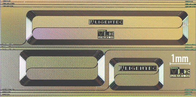
LIGENTEC’s silicon nitride small footprint AWGs, phase shifters and splitters for telecom SiN platform. Image by Belen Lopez-Fuchet, LIGENTEC
Since its inception, the company has focused on meeting design and product development needs across the supply chain while maintaining their connection to photonic researchers and R&D facilities across Europe and other centers of photonic excellence.
“LIGENTEC customers are large corporations as well as smaller, high-tech companies and R&D centers. The low propagation loss of our SiN-enabled devices, together with high power level operation makes the platform unique for market areas such as laser metrology, microwave photonics, LiDAR, AI and 5G. The possibility to generate photon pairs on the chip together with the low propagation loss is very interesting for quantum applications. The large transparency window from the visible to the mid-infrared allows a SiN-based PIC to enter markets in bio sensing and gas-sensing,” he added.
Beyond the flexibility of working with a company built to serve organizations of all sizes, Geiselmann said they continue to appreciate that while some customers are large, many are SMEs and customers also include research organizations that work with limited budgets.
“LIGENTEC offers an all-nitride-core foundry service with a fast turn-around time. There are two standard processes specifically engineered for customer applications in the visible and the IR, with their respective PDK and process modules. This enables a fast prototyping of the desired PIC-based product. Furthermore, LIGENTEC offers a low-cost access to the all-nitride-core technology using the cost sharing model of multi-project wafers (MPW.) The platform can provide low propagation loss PICs (<0.1dB/cm) and is transparent from the visible to mid-infrared (400nm-4000nm). LIGENTEC is fully committed to offer a platform forging strong partnership agreements with key players in the photonic ecosystem, providing our customers with the entire validated supply chain,” he said.
Low loss compact delay lines with losses below 5dB/m. Image by Belen Lopez-Fuchet, LIGENTEC
As an exciting new branch within the global photonics industry, PIC device designers and manufacturers are still working through the processes of taking their designs and products from low-level, manual assembly and test to higher production levels including packaging pilot lines. Most companies across the industry agree that standardized test, assembly and packaging (TAP) is a goal all can support since achieving it will help ensure quality and reduce device failures in the field, as well as help achieve the cost objectives of datacom, telecom and other price sensitive customers. Geiselmann explained that while LIGENTEC is not yet packaging devices in-house, they have established a qualified partner network and are ever mindful of the need, supporting local and industry-wide efforts to standardize and automate operations.
“LIGENTEC takes reliability and quality assurance as a top priority for large scale adoption of PIC. To that end we are enhancing our effort on statistical control of our models and are establishing collaboration agreements with research centers to stress-test our components in all relevant environments. For example, SiN resonators were exposed to proton radiation for space applications. LIGENTEC passive circuits have a very low failure rate due to dedicated development and testing of the PDK.”
“LIGENTEC’s SiN platform offers spot size converters that make packaging to SMF28 fiber very efficient. Furthermore, LIGENTEC’s platform offers the capability to have several SiN layers implemented to enable 3D photonic integrated circuits. Furthermore LIGENTEC chips can be operated as interposer chips with record low loss coupling levels for hybrid integration,” he said. LIGENTEC is already looking at ways to enhance its portfolio and as it works more with customers is addressing unique needs as well as working to satisfy requirements within long-established applications.
“LIGENTEC has developed a PDK for telecom wavelength and visible wavelength for bio-sensing and microsopy. Additional modules are available to integrate metal layers for phase shifters and switches as well as cladding opening for bonding other PICs or sensing applications. LIGENTEC operations are based on industry standards of using SPC and Cp, Cpk to control process performance. Our processes come with a rigid set of quality control to ensure guaranteed geometric accuracy and high performance. In addition to that we actively invite our customers to influence our R&D roadmap to develop a technology portfolio that is market relevant,” Geiselmann added.

AWG for visible wavelength operation for LIGENTEC’s visible SiN platform. Image by Belen Lopez-Fuchet, LIGENTEC
For further information about the advantages of silicon nitride (SiN) based PIC component design and foundry services, visit the company website at www.ligentec.com, or email them at:
info@ligentec.com
Eindhoven University of Technology is positioning itself as one of the global leaders in extremely low latency 5G link technologies. PhotonDelta’s Jonathan Marks recently spoke with Professor Idelfonso Tafur Monroy, who heads the BluesSpace Public Private Partnership. His expertise in microwave photonics is also a key part of one of the Photonic Integration Technology Centres now being established within the PhotonDelta ecosystem. With several major photonics events scheduled for the coming months, we asked Idelfonso to explain ways in which 5GPhotonics will revolutionize several emerging high-tech sectors.
“Today our mobile phone infrastructure operates with the fourth Generation (4G) standard,” explains Idelfonso. “We expect significant rollout of 5G in Western Europe around 2022, with many public demonstrations during the European football championships in 2020, just over two years from now. But a lot of technical challenges need to be solved before then.”
“The infrastructure needed to support 5G is going to be massive. It is beyond what most people can comprehend - and that includes many industry specialists. Remember the telecom industry has taken the 4G capacity and transmission norms from 2010 and set themselves the goal to make the new 5G network 1000 times faster, reaching 7 billion people while using 90% less energy.
Professor Monroy explained that for many decades, research teams in Eindhoven have been taking an active role in tackling those technical challenges. But now researchers are going beyond just being a lead partner in several international projects. They are developing a test-bed to demonstrate that these technologies work to solve many real-world challenges.
The 5G link with Robotics & Autonomous Cars
“As well as mobile telecom, photonics and high capacity optical fibre infrastructure is crucial for other areas that demand reliable, instantaneous connectivity.”
“Take smart factories, for instance. It is becoming important for robotic devices to collaborate in real-time with each other. Robots will also need to interact with human operators, video cameras and sensors. And the connection between these robots is going to be based on 5GPhotonics because only “instantaneous” technologies can provide the low latency requirement as well as robust, secure and reliable connectivity. In these situations, you cannot afford to have any down-time or intermittent connections.
Many of these robots will need to access video or images that are stored in the cloud, i.e. on data servers that could be physically tens of kilometres away. 5GPhotonics is key to addressing the issues of having sufficient bandwidth between the robot and the server in the cloud, as well as ensuring the very low latency. Once this is working it is easy to extrapolate that scenario to autonomous agricultural robots. This is also relevant for robots that need to cooperate for search and rescue in natural disaster recovery or dangerous demolition tasks.”
Professor Monroy explained further that researchers are investigating ways in which they can team up to solve some of the challenges ahead for the automotive industry. In autonomous driving, low latency with extremely robust, secure network connections to edge computers operating in the cloud is very important. The scale of that network is very large.
At the CES consumer technology show in Las Vegas back in January 2018, the technical press noted that while the current LIDAR technologies work on the highway, the car navigation systems seem to get confused in urban settings with a lot of pedestrians, cyclists and tall buildings. 5GPhotonics can also play a role here, because there’s a similar need for instantaneous, high data-rate, secure, robust connections between cars and control centres.
“Our contribution from Bluespace will be our knowledge of the K-band wireless technology combined with the multicore fibre infrastructure running to the sensors on top of street lampposts. And the University campus is an ideal testing ground since it already is a ‘city within a city’.”
Building Eindhoven’s large photonics demonstrator
“You may remember that 10 years ago, the European Laboratory for Particle Physics CERN in Switzerland started operation of the Large Hadron Collider. It’s the world’s largest and most powerful particle accelerator, built to test and demonstrate various theories in particle physics. The LHC consists of a 27-kilometre ring of superconducting magnets surrounding the city of Geneva, with many accelerating structures to boost the energy of the particles along the way.”

“In a similar vein, we need a testbed to demonstrate the capabilities of light-based technologies to both research institutions and large enterprises. There is also going to be an extremely fast optical-fibre ring built around the city-centre campus of Eindhoven University of Technology. Our Bluespace 5GPPP project has been allocated four empty ducts in this ambitious project. Very soon we hope to be one of the first to deploy cables composed of next generation multicore optical fibres. Large spools of these cables have been developed in our labs in the University’s Flux building. But now we will be able to test their performance under real-world deployment conditions,” he said.
Rollout of fibre-to-the-antenna
“To be an interesting proposition for the mobile network operators, as well customers, we are working on a different architecture for 5G. For instance, today many mobile base stations use electronic switching inside the base station mast and then convert this to an optical signal at the base where the fibre comes in. It turns out that this is one of the biggest bottlenecks in the 4G network. So, we’re looking at bringing the fibre all the way up the mast and connecting it directly to the smart base-station antenna. To the reduce power consumption by the network, our teams are involved in designing smart antennas that can beam a more concentrated signal in the direction of the mobile phone user.”

“We are working with a UK company called Optoscribe that is making the connections between standard single core optical fibres and our new multicore solutions which may have as many as 19 cores inside the same cable. These multicore cables carry many times more data bandwidth but require newly designed components to connect them, like fan-in, fan-out, splitters and combiners. Our goal in Bluespace is to build multiple cores into one single fibre without enlarging the diameter of the cable Of course, we’re not trying to do this alone. We’re pleased that we’re able to enter into a technology transfer agreement with Corning that has become a major partner within Bluespace.”
“Consumers know Corning as the developer of Gorilla Glass for mobile phones. But they are a major force in specialty glass and optical physics. We anticipate these multicore products will come onto the commercial market within the 3-year projected lifespan of the Bluespace project. They will be used to directly feed optical signals to the antenna of a base station. In Eindhoven University of Technology, we will focus on providing fast, low latency links and then develop the secure connections to support robotics and LIDAR applications.”
“We had the second and third technical meetings of the Bluespace project in December 2017. And now we’re going to start defining the verticals for the demonstration of the Bluespace capabilities. The website for the demonstration is at Eindhoven University of Technology. Work on that starts soon - expect that to go live in mid-2019. And the results are also going to be demonstrated in the laboratories of the largest Greek telecom operator Cosmote.”
What about the intellectual property being generated?
“For the moment most partners develop their own IP, but the benefits of the recently launched PhotonDelta IP cloud and the cooperative appear very stimulating. We’re going to organize special workshops with the researchers to explain the benefits of this unique IP cloud approach. It’s a good idea specifically for the type of innovation that requires a very fast development because of the limited product lifecycle.
Many of the algorithms used in big data collection require a type of data analysis, processing and interpretation that needs to be ultra-fast. It is very important that we develop these capabilities ourselves as fast as possible. If you wait, then it could be too late.”
“It reminds me of the speed that was required five years ago with the development of apps for the mobile phone. You cannot afford 2-3 years to develop an app. It is the same here. If you know how to increase the speed and accuracy of positioning algorithms, then sharing the concept in the IP cloud is a very good way to find collaborators and develop the prototype much faster. For some other types of core development, you may want to take the more traditional patent route. But one approach does not rule out the other.”
“We are setting up what we call the Tu/e 5G testbed. It’s going to be composed of the new optical ring that will surround the University campus with tap-in and tap-out points in the lampposts. The multicore fibre will be used to connect the laboratories in the University’s Flux building with a 5G base station in the campus. We’re aiming to build a network that will support 125 GB/second. We will use multiple array antennas which should deliver a wireless speed of around 10 GB/sec to mobile devices.”
“We will be able to connect to other nodes around Europe so that there will be ways for our partners to access the demonstrator remotely. So, let’s says you are developing a new model for support in the backhaul/fronthaul - that can be tested here. Or you might be developing optical routing nodes and modules for the edge computing. That can also be tested here. And we envision connecting these 5G optical fibre base stations with an optical outer ring. This will be about 40 kilometres of fibre around the city of Eindhoven and that will become the basis for a quantum key-distribution testbed. So, the clients of the Photonic Integration Technology Centres in the Netherlands will also have access to the facilities for developing photonics for Quantum Key Distribution and for 5Gphotonics communication to be tested here as well. Our contribution is being able to offer PITC customers access to an infrastructure which allows for real-world testing in urban conditions.”
Showcase 2020
High-profile trials demonstrating technology now in development and accessible to large public audiences are planned in two years. The target flagship event should serve as a milestone for industry, governments and the general public, showcasing the benefits for individuals and society. The UEFA EURO 2020 football championships will be played in 13 different cities in Europe (Glasgow, Dublin, Copenhagen, Budapest, Bucharest, Brussels, Bilbao, Amsterdam, Saint Petersburg, Rome, Munich, Baku and London). This makes the EURO 2020 an excellent opportunity for a 5G Pan-European trial, also because of the media attention it will get. The timing of EURO 2020, in the summer 2020, is just prior to the 2020 Olympics in Japan. Several 5G services will be trialled around the EURO 2020 football cup.
Three different types of trial services are proposed:
In the vicinity of stadiums and in fan zones, 5G augmented and virtual reality applications related to EURO 2020 or football in general can provide ways to entertain fans before, during and after the game, including immersive experiences around the competition. These services are not confined to the hosting cities.
EURO 2020 will be the opportunity to demonstrate services in autonomous transportation around the stadiums and relevant transport routes. Scenarios include transportation to and from the airports and automated vehicles for the transport of officials, staff and supporters.
Public safety authorities dealing with security around the stadiums could benefit from Advanced public safety services. Augmented reality can be used to visually mark and track persons of interest based on facial recognition. Tailored services (e.g. access security, person localization) will create a significant higher level of both safety and security.

Professor Idelfonso Tafur Monroy
Professor Monroy leads one of the many projects that are underway at the Eindhoven University of Technology designed to address the challenges and opportunities of bringing high speed, wide bandwidth photonic integration together in future data networks that deliver faster throughput while utilizing less energy. One important aspect of these programs is the incorporation of integrated photonics into future 5G mobile platforms.
PhotonDelta is an international professional organization. Established as a project in 2016, PhotonDelta became a fully-fledged foundation on December 13th 2018. We’ve developed a secure IP cloud. This forms a trusted network of industry and research institutions united in the goal to accelerate the adoption of photonic systems across a wide-range of new products and services. Headquartered in Eindhoven, The Netherlands, we match break-through innovation found in young scaleup companies with the experience of universities, photonics enterprises and corporate research centres. We are funded through the Dutch national PhotonDelta Public Private Partnership 2018.
Photon Delta and the To-Euro-5G H2020 project (with support from the European Commission) has released a new video detailing 5GPPP initiatives. Learn more about the 5GPPP program and its focus on photonic integration technologies:
Silicon photonics technology has definitely reached a first level of maturity, as it can be found nowadays in commercial products for intra- and inter-datacenters communications at high data rates. Higher volume markets such as intra-rack communications could be addressed by solving three main challenges: the packaging, the energy consumption, and the laser integration.
By Karim HASSAN, PhD, Researcher and Project Manager at CEA-Leti
The convergence of photonic technologies into a CMOS compatible silicon photonic platform remains a key challenge while several fabrication supply chains and industrial products are available in the field of high speed communications on optical fiber. Nowadays, the circuit design tools are available on several software platforms. However, silicon photonics is still suffering from the lack of integrated light sources. Existing packaging solutions offer a straightforward way to combine III-V laser sources and silicon photonics integrated circuits in order to address the market today, at the expense of a high cost and low volume production. On the other hand, the hybridization of III-V gain material (which remains the materials of choice to achieve semiconductor laser sources) can be realized using III-V direct bonding on top of patterned silicon. Subsequent laser demonstrations relying on CMOS-compatible process for the silicon part have been in most cases followed by process steps carried out with small wafer III-V fabrication lines (typically below 4-inch wafers). With such integrations, the cost advantage of silicon photonics based on the use of CMOS platforms and large wafer format is not valid.
The issues regarding the integration of III-V material go beyond the introduction of the material itself on CMOS lines. In fact, fundamental aspects such as having a low access resistance with CMOS back-end of line (BEOL) metals onto III-V compounds is not straightforward since noble metals, e.g. gold, cannot be used. The thin SOI (<310nm) used for getting single mode silicon photonic integrated circuits (PICs) makes optical coupling with the thick III-V gain material (>2µm) difficult. It is worth noting that the topology of III-V components, having a large height of about 3µm, makes the co-integration within the BEOL of active silicon devices interconnects incompatible.
Furthermore, while large format of III-V wafer epitaxy is still in progress, most of the III-V suppliers can provide laser stack onto wafers smaller than 4 inch, which makes the use of dies rather than wafer mandatory for the hybridization on 200mm silicon wafer (as well as 300mm).
Nevertheless, the use of III-V dies generates additional difficulties for III-V processing due to undesired lateral etching of the dies during the III-V substrate removal. An overall integration strategy must be developed in order to solve these technological barriers.
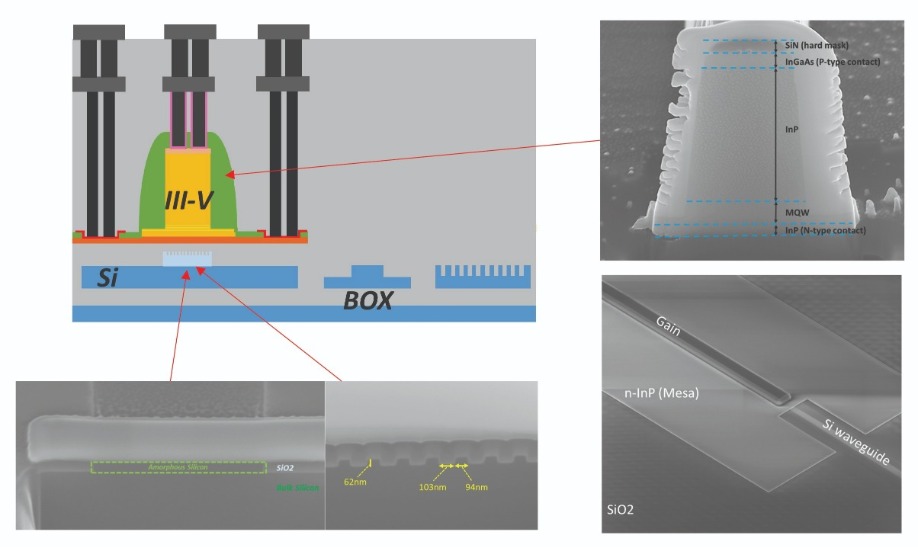
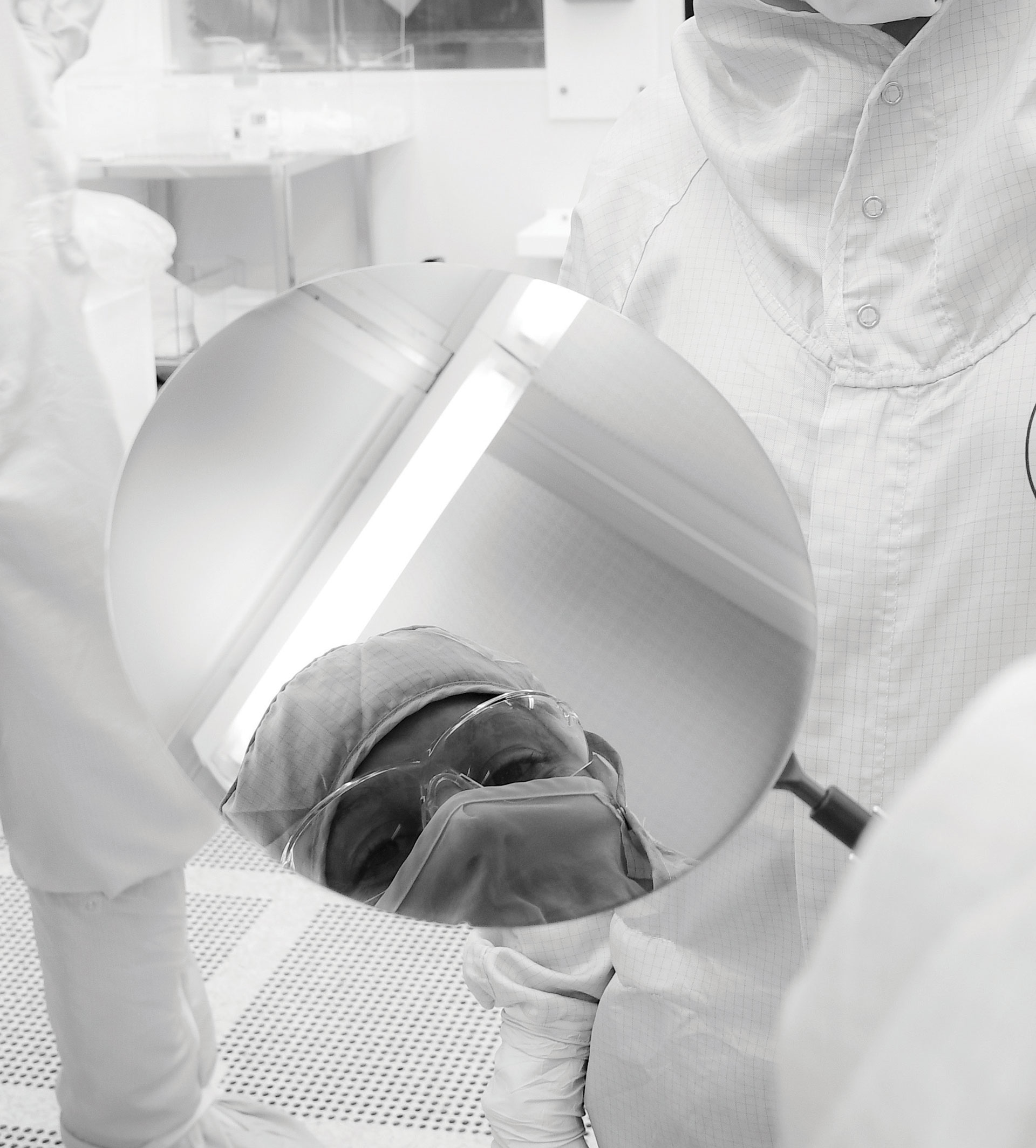
Figure 1. Schematic view and scanning electron microscopy images of III-V on silicon laser fabricated on 200mm CMOS lines.
In order to break the existing technological limitations for mass production of hybrid PICs, CEA-Leti’s R&D fabrication platform has developed a first laser integration on a 200mm fully CMOS-compatible silicon photonics platform, as depicted in the Figure 1.
The fabrication process can be divided into three main parts, with first the silicon patterning followed by the III-V hybridization through molecular bonding, prior to the III-V patterning (including the CMOS metallizations). The optical coupling between III-V and silicon requires thick silicon waveguides, which is obtained by a localized thickening with amorphous silicon, as shown in Figure 1. Next, a chemical and mechanical planarization (CMP) is used to provide a smooth oxide layer for the direct bonding of III-V on silicon. The novel patterning of the III-V material that has been developed relies entirely on the 200mm platform. The new process flow proposed by CEA-Leti uses selective reactive ion etching (RIE) steps on both p-InP and p-InGaAsP.
New BEOL for lasers
Such a new patterning sequence allows us to encapsulate the III-V completely prior to the BEOL, which will remain planar, similar to standard silicon photonics components. Consequently, a high density of vias can be patterned on the SiO2 encapsulation and subsequently filled with tungsten on top of both contact sides made of Ti metallization deposited by magnetron sputtering (PVD), prior to the final AlCu micron-thick pad layer, as depicted in Figure 2.
This new CMOS BEOL for lasers, developed within the framework of the IRT Nanoelec Photonic Program, a French consortium involving CEA-Leti, ST Microelectronics, ALMAE, CNRS-LTM, and Mentor Graphics, results in a state-of-the-art serial resistance on hybrid lasers ranging from 3 Ohms to 4 Ohms.
Large scale automated testing
Large scale automated testing is also of great interest when arguing about large volume production of hybrid PICs. Thanks to the novel 200mm process, full wafers can be thoroughly mapped with electro-optical fiber-to-fiber measurements. Such a test is made possible by the use of fiber grating couplers fabricated onto the silicon, similarly to standard silicon PICs. Most of the developments required specifically for the tests of hybrid lasers relies on the spectral (CW and pulsed) and thermal characteristics. Even though silicon devices are also sensitive to temperature variations, the behavior of hybrid lasers regarding thermal fluctuation and the aging of such object is vital to ensure the operability on datacenter environments.
There are still some challenges in this regard to provide high temperature tests before the packaging, with, for instance, the improvement of optical fiber position and vibrations due to convection over the wafer and dilation of it. The development of on-wafer laser testing is not only relevant for the monitoring of the fabrication yield, but also for sorting out the hybrid photonics chips as a function of their performances before packaging.
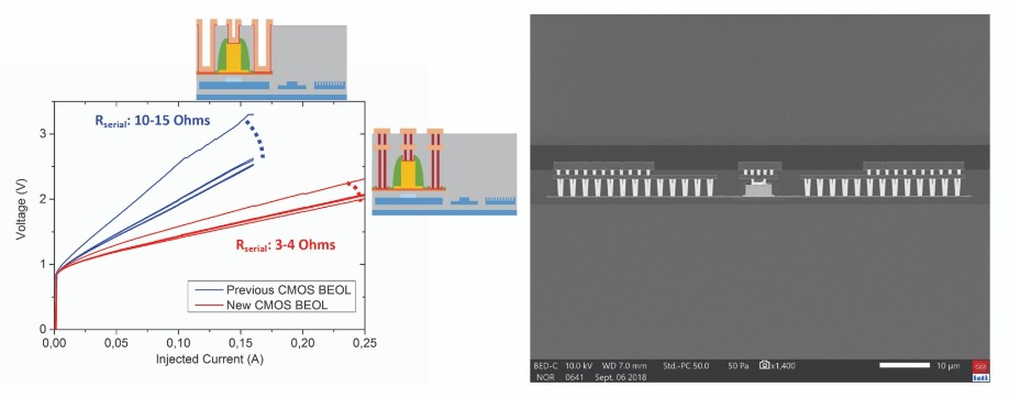
Figure 2. Experimental IV curves on 200mm CMOS hybrid lasers with 1 and 2 levels of BEOL and scanning electron microscope view of the cross-section of such laser developed on CEA-Leti’s R&D fabrication platform.
Beyond the performances and efficiency, the cost of hybrid III-V/Si transceivers is of great interest. While mass production of silicon chips is cheap, the addition of III-V materials can increase significantly the budget per PIC. One can note that the consumption of III-V material must be minimized in order to reduce the environmental impact (by the material itself or the chemicals used for waste treatment). Figure 3 shows 3 mm x 3 mm III-V dies on top of a 200mm SOI wafer (including silicon photonics circuits for high lasers) after the molecular bonding. The newly developed 200mm die bonding reached a yield ranging from 70 to 99%, with 90% of the successfully die transferred having 99% of III-V material bonded onto the SOI surface. While the molecular bonding itself can be executed the same way as wafer bonding, the substrate removal is more critical for dies due to undesired lateral etching.
The thinning was ensured by first an original sequence of grinding operation down to 50µm III-V remaining prior to a chemical wet etching used to remove the remaining part of the substrate. By adding a grinding step before the wet etching, the lateral consumption of III-V during the substrate removal was reduced by a factor between 3 and 5. The III-V patterning on those dies is now in progress to realize hybrid lasers.
Conclusions
Recent developments led by CEA-Leti within IRT Nanoelec have led to a full CMOS friendly laser integration process, exhibiting very low serial resistance thanks to novel contacts metallurgy. In addition, wafer scale approaches allows high yield bonding of reduced area III-V coupons/dies onto SOI wafers, drastically reducing the cost of next generation photonic transmitters. The scalability towards 300mm for both CMOS contacts and die bonding is currently under development, paving the way for the adoption of silicon photonic technology in a variety of emerging applications such as system in a package photonic transceivers, high performance computing and PIC based LiDARs.
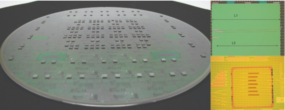
Figure 3. III-V dies on 200mm silicon wafer, and microscope images of such die after the III-V substrate removal and during the 200mm CMOS process of hybrid lasers.
References
CEA Tech is the technology research branch of the French Alternative Energies and Atomic Energy Commission (CEA), a key player in innovative R&D, defence & security, nuclear energy, technological research for industry and fundamental science.
CEA was named by Thomson Reuters as the second most innovative research organization in the world in 2017. CEA Tech leverages a unique innovation-driven culture and unrivalled expertise to develop and disseminate new technologies for industry, helping to create high-end products and provide a competitive edge.
Follow us on www.leti-cea.com and @CEA_Leti
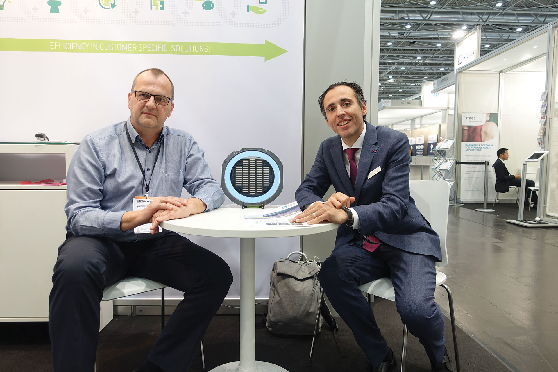
If you are looking for expert help with wafer treatment, preparation and packaging, offering advice on product and process development as well as volume production - all from a one-stop-shop, then AEMtec could be your solution. In this article, Jose Pozo (Director of Technology and Innovation at EPIC) talks to Matthias Lorenz, head of AEMtec’s business development in North America about how AEMtec can help with application development and innovation in the photonics sector.
Background
AEMtec was set up in 1989 as a back-end group by Siemens Infineon mainly using wire bonding and fibre optics technologies for data communication systems. In 2000, they became an independent contract manufacturer and have since transformed themselves into an E2MS company - an engineering and electronic manufacturing service supplier. With this move, using their wealth of experience and specialist know-how, they were able to complement their manufacturing capability with a range of services covering all stages from product development to volume production - all from a single source. Headquartered in Berlin, the company ensures effective service delivery through a workforce of 180 with 45 engineers dedicated to process development, process improvement and reliability improvement.
Current product lines
AEMtec’s key product lines are currently high-precision placement for optical components for the semiconductor equipment industry, for example photolithography stems and mask writers. Another of their strengths is in the medical imaging sector, and involves the population of various types of ceramic substrates for applications in computer tomography as well as for ultra sound imaging for cardio and other health monitoring. They are also in the business of data telecommunications, especially customised devices such as cross-connect centres and special high-speed applications. Additionally, they are specialists in customizing imaging and other types of sensors that require a particular kind of packaging technology. For Matthias, AEMtec’s main strength is their ability to help customers improve the reliability of their products through the use of a comprehensive range of dedicated processes and packaging technologies from a single source. This avoids the need to outsource, which is not only more expensive but can also jeopardise product reliability.

Fig 1. Matthias Lorenz, head of AEMtec’s business development in North America and Dr. Jose Pozo, CTO of EPIC, the European Photonics Industry Consortium.
Services for the photonics sector
One of the key challenges for the integrated photonics sector is the long turnaround time for some components from design to packaging, which can range from 6 months to a year or even longer. These long lead times, impacting directly the time to market, are detrimental both for the development of new applications and for innovation in general.
A case in point is the turnaround time, typically 12 to 18 weeks, for wafers between the moment when they leave the foundry until the chips of these wafers are ready for packaging. These long lead times are due to the various procedures required to prepare the wafer for population. These processes typically involve under bump metallization (UBM) done in layer of different metals like Ni/Au or Ni/Pd/Au followed by micro solder balls attachment, and then grinding, testing and dicing. In most cases, the supply chain is fragmented, the handling of various suppliers is tedious, time consuming and can also affect reliability.
In answer to this problem, in 2016, AEMtec opted for a backward vertical integration by expanding the range of services to include all wafer back-end processes, thus creating the most complete range of technologies in the industry, for small and medium volumes. Thus AEMtec takes full responsibility for all the processes required for getting the wafers out of the foundry, treating them and introducing them to the assembly lines. UBM, solder ball attachment and dicing are performed in-house and the grinding and testing are outsourced to reliable experienced companies. Amazingly, this service has reduced lead times from 12 to 18 weeks to less than 18 working days.
This is a huge benefit for their customers both in terms of reducing costs and reducing time to market. For Matthias, time to market is key, particularly for the photonics industry, because there are a lot of sector ‘hot spots’ spread over North American, Europe and especially Asia. “Speeding up wafer treatment and preparation for packaging is a big advantage because it enables customers to obtain faster feedback on the functionality of the device and the opportunity to improve wafer design and even the device itself.”
VCSELs gained renewed notoriety in 2018 thanks to their use in high-end smartphone facial recognition applications. Alignment and packaging plays a critical role in each finished module that can involve 300 or more individual VCSEL die.
Automated packaging
Packaging of opto-electronic components, including single dies, and photonic devices is one of AEMtec core businesses and Matthias believes that AEMtec is unique in the technologies they offer. After evaluating the strengths and weaknesses of passive vs. active alignment, they opted for passive alignment and have a variety of equipment in-house which is capable of handling placement accuracies down to 0.5 microns. But, he adds, “the real key is not the placement accuracy itself, it’s the expertise in handling the components, the equipment and the consumables.” The crucial feature of good packaging is that the process is stable and reproducible for future volume production and thereby avoids any return merchandise authorizations (RMAs) from the customer.
One of the difficulties for packaging houses in Europe in achieving placement accuracy, whether by active or passive alignment, is that some of the externally sourced components have imperfect substrate surfaces, which makes a consistent placement accuracy of 0.5 microns difficult to obtain. Being a one-stop-shop, this is not a problem for AEMtec. But as Matthias points out, accuracy is not just a matter of equipment and components: of equal importance is the process, the environment and the type of substrate the customer selects. These all vary according to individual requirements and in turn, determine the type of packaging technology. Matthias sees AEMtec’s role as similar to the conductor of an orchestra. “If the violins are the components, the brass instruments the consumables and the wind instruments the substrates, then like a conductor, we try to get the best sound from each combination of the individual instruments.”
FDA approval
While many of the products that AEMtec produces are used in medical devices that have to go through the FDA approval process, as an independent contract manufacturer, AEMtec cannot assume responsibility for product release and the company is therefore never directly involved in the FDA approval process. However, in accordance with current medical device regulations (MDRs) and the new revised FDA regulations, they can help customers with all the administrative paperwork in relation to reliability testing and clinical studies.
AEMtec supports a wide range of medical devices and can assist customers with the administrative paperwork associated with reliability testing and clinical studies.
As an end note, and with an eye to the future, AEMtec is currently investigating the silver sintering technology applied to optical products, as a viable alternative to the soldering process, especially for high temperature/high pressure applications. AEMtec shares the opinion that this ‘fully clean/no residues’ process may be the better alternative, also due to the lower remnant mechanical stress for 3/5 and 2/6 materials (compared to TS/TC processes), and it is therefore investing resources in the technology in order to be ready for the next step.

Jose Pozo is Director of Technology and Innovation at EPIC (European Photonics Industry Consortium). He has a 20 year background in photonics technology and market knowledge, and a large network within the industrial and academic photonics landscape. Jose is a member of the board of the IEEE Photonics Society Benelux. He holds a PhD in Electrical Engineering from the University of Bristol in the United Kingdom and an MSc and BEng in Telecom Engineering from Spain/Belgium.
AEMtec develops, qualifies and manufactures next level optoelectronic assemblies in compliance with highest quality, security and sustainability standards. In a cleanroom environment (ISO class 5 to 8), AEMtec offers a unique spectrum of high-end chip-level technologies: Wafer Back-End Services (UBM, SBA, Au Stud Bumping, Dicing), high speed / high accuracy Die- and Flip Chip Bonding, Au and Al Wire Bonding, SMT, assembly of Optical Components, Box-Build, 3D integration. AEMtec is certified for medical industries.
www.aemtec.com
By Callum G. Littlejohns, PhD Optoelectronics Research Centre (ORC), University of Southampton, UK
The Silicon Photonics Group at the University of Southhampton (UK) is delighted to offer the unique opportunity of bespoke PIC design training courses, crafted specifically to meet a company’s unique needs and interests. The training is supported by some of the world’s best academic fabrication capabilities and by 30 years of research excellence in state-of-the-art facilities.
The Silicon Photonics Group is internationally-known for its track record of world-leading results and comprises more than 50 members with expertise across the PIC field; from device simulation and design to advanced fabrication techniques and device characterisation.
CORNERSTONE is a silicon photonics rapid prototyping multi-project-wafer (MPW) capability that utilises industrially-compatible tools (e.g. deep-UV projection lithography), to enable seamless scaling-up of production volumes, whilst also retaining device level innovation capability using high-resolution lithography (e-beam) and versatile processes.
The PIC technology platform is a collaboration between the Universities of Southampton, Glasgow and Surrey in the UK, with the majority of the processing taking place in the Optoelectronics Research Centre’s cleanrooms at the University of Southampton, where a 248nm Nikon Scanner is installed. The unique hybrid processing (DUV projection lithography and e-beam lithography) capability renders the CORNERSTONE platform attractive to both academia and industry, and is able to mimic advanced industrial processes.
Presently, CORNERSTONE offers 3 different silicon-on-insulator platforms (220nm Si / 2µm BOX; 340nm Si / 2µm BOX; and 500nm Si / 3µm BOX), enabling a plethora of applications including telecoms, mid-infrared sensing, etc. The unique hybrid processing (DUV projection and e-beam lithography) capability renders the CORNERSTONE platform attractive to both academia and industry.
CORNERSTONE is an open access technology which operates approximately 6 MPW calls per year, in addition to bespoke fabrication batches (available on request). The design rules, schedule and cost, mask submission forms, and terms and conditions can all be accessed via the CORNERSTONE website: www.cornerstone.sotonfab.co.uk
Bespoke training can be tailored to support needs in any aspect of photonic integrated circuit (PIC) design, and is offered in parallel to the group’s rapid prototyping multi-project-wafer (MPW) capability, CORNERSTONE. Members of the training team will work with you to build a curriculum around your precise requirements, giving you the opportunity to specify which topics should be covered, the duration of the course and venue, etc. Potential topics include:
Participants will also have the chance to visit Southampton’s cleanroom complex and experience live device fabrication using advanced, industry-compatible, deep-UV projection lithography, amongst other fabrication tools.
Training can be integrated into any of the CORNERSTONE MPW fabrication batches on various silicon-on-insulator (SOI) platforms, including state-of-the-art modulator design, fabrication and characterisation, or offered as a stand-alone course.
Characterising a spiral waveguide
An example training course which includes designing your own PIC’s, is as follows:
Initial content offered over four days:
Follow-up day:
Utilising patented self-alignment processing technology, the CORNERSTONE team have designed silicon carrier depletion modulators with data rates of beyond 56 Gbit/s. With four implant layers, three silicon etch depth and metallisation steps, these designs are available in active device MPW calls. Additionally, more frequent passive, or passive-with-heater, MPW calls enable the fabrication of complex silicon photonics circuits, with single mode rib waveguide propagation losses as low as 2.5 dB/cm, and using the hybrid high resolution e-beam lithography layer, high efficiency grating couplers with insertion losses < 1 dB.
The CORNERSTONE PDK is available using Luceda’s IPKISS platform www.lucedaphotonics.com, or in gds format on the CORNERSTONE website. All designs are open access.
A programmable photonic integrated circuit (PIC).

Dr Callum Littlejohns is a member of the Silicon Photonics Group’s fabrication team, and the primary point of contact for both CORNERSTONE and PIC training. He has a track record of excellence, having received multiple awards throughout his academic life, including the Information Overload category winner at the 2015 EPSRC ICT Pioneers Award.
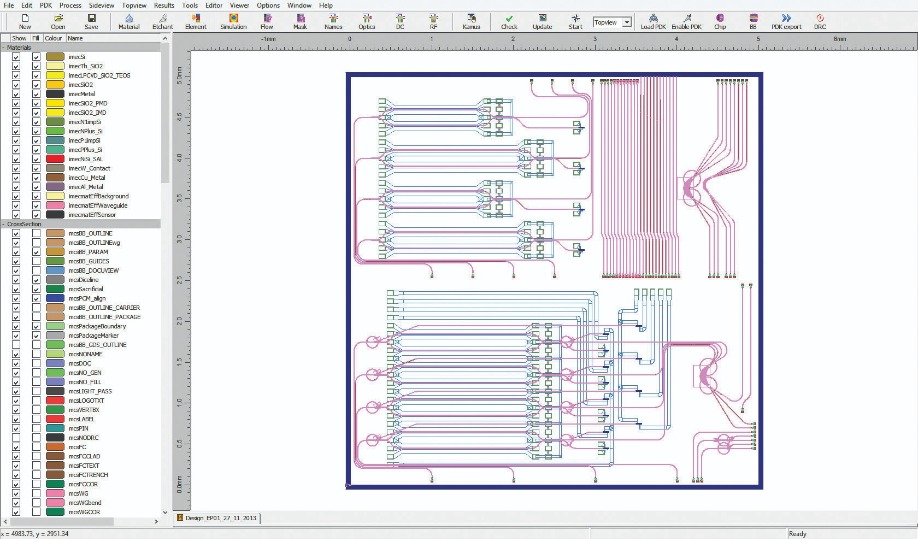
Synopsys is defining a new era of photonic circuit design with unified flow and custom process design kit (PDK) support. Company experts and invited speakers will present an immersive, hands-on workshop the week before the PIC International Conference to teach designers how to navigate this new era of photonic circuit design. PIC Magazine invited Niek Nijenhuis, Global Business Development Manager of Photonic Solutions at Synopsys, to discuss how the workshop will benefit photonic circuit designers.
One of the challenges faced by photonic foundries and PIC designers is the disconnect between the pace of technological advances in the industry and the readiness of photonic design automation (PDA) infrastructure. Synopsys is driving the advancement of PIC technologies with its PIC Design Suite, which comprises the OptSim Circuit and OptoDesigner tools and supports a wide range of application requirements, from data communications to sensors and biomedical devices.
The suite offers a seamless PIC design flow from system-level design and verification through PIC design capture, layout, verification and manufacturing, as well as access to a single, world-class support channel.
Synopsys’ PIC PDA suite also works seamlessly with OptSim, the company’s industry-leading telecommunications and data communications photonic network modeling tool. OptSim comes with a rich library of photonic and electronic components, stimulus generators, and analysis routines, which can be used to model any photonic communications network. It shares a graphical interface with OptSim Circuit that allows the custom PIC to be simulated in context with the rest of the full photonic network.
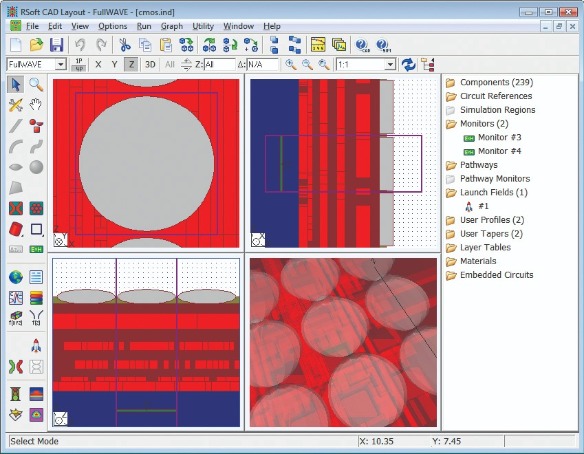
A view from RSoft CAD Layout – FullWAVE
Utilizing OptSim Circuit from Synopsys, designers can model and optimize PICs at the system level, including coupling and feedback of optical and electrical signal paths.
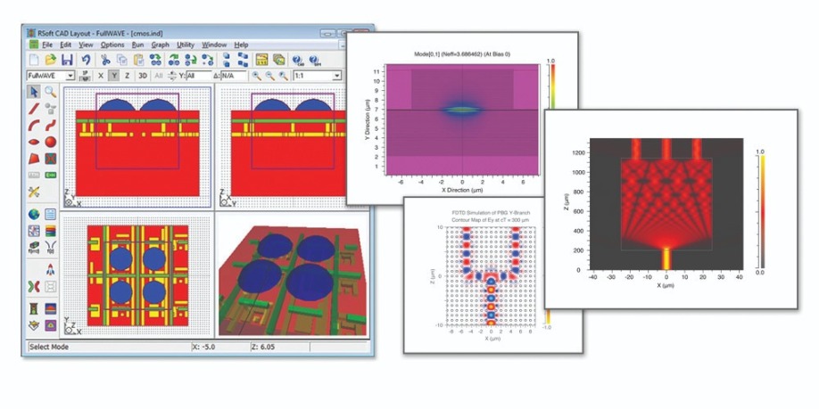
Synopsys highly flexible software suite allows designers to select from the industry’s largest portfolio of photonic device simulators to design waveguides, nanostructures, and other components for new PICs.
In addition, talks by foundry representatives will provide information about their specific PDK offerings and capabilities, and will give designers guidance for obtaining PDKs and participating in multi-project-wafer (MPW) runs to verify their ideas through manufacturing.
PIC designers can access photonic-aware physical layout capabilities to synthesize PIC layouts for fabrication, enabled by support for foundry-specific PDKs.

Photonic integration has taken many forms and is evolving even as first-generation PICs are entering data centers. 2018 PIC International Conference award winner Ayar Labs brings its novel approach to integrating electronic and photonic architectures in the race to create tomorrow’s data superhighways.
By Mark Andrews, PIC Magazine Technical Editor.
Technologists envision a future where autonomous vehicles, 5G mobiles, IoT-enabled sensors and a plethora of other innovations create, analyze and share data seamlessly. What is spoken of less frequently is the fact that the ‘lanes’ of our data highways are clogged. Without a fix, our data-intensive dreams may remain only that. And without resolution, today’s digital highways will see slowdowns, data caps and congestion.
But fear not – PICs are coming to the rescue!
Put another way, the world’s data infrastructure for moving massive amounts of digital content from every point imaginable to every destination imaginable is running on fumes. The exponential growth of data is slowing processing times. This hampers the abilities of data center, telecom and broadband infrastructure to accelerate uploads and downloads. While mobile 5G systems are designed to increase capacity and reduce slowdowns, how will all that 5G data reach its intended recipients? No matter where our bits and bytes originate, everything passes through data centers, nodes and switches at some point along the road. In a very real sense, the data center corundum affects every digital data user.
Moving data with photonic technology is of course not new. Fiber optics has been utilized for years and the migration towards optical transport began when telecom providers started sending signals across long distances; subsea optical fiber has been replacing copper wires for decades. Optical solutions are now seeing deployment between and within data centers. But in the future Ayar Labs and other innovators see this approach as coming all the way into computer servers, racks and ultimately into the processor chip packages themselves, which is a major focus of Ayar’s work. Another data point that differentiates what Ayar Labs does is that today most of the photonics industry focused on serving data centers is developing products that enhance or replace pluggable transceivers, whereas Ayar Labs is focused on ‘chip-to-chip’ photonic integration – if successful, this approach could transform the market, making the opportunity much larger than existing levels of optical deployments, with some analysts arguing the market could grow three to four times its present size.

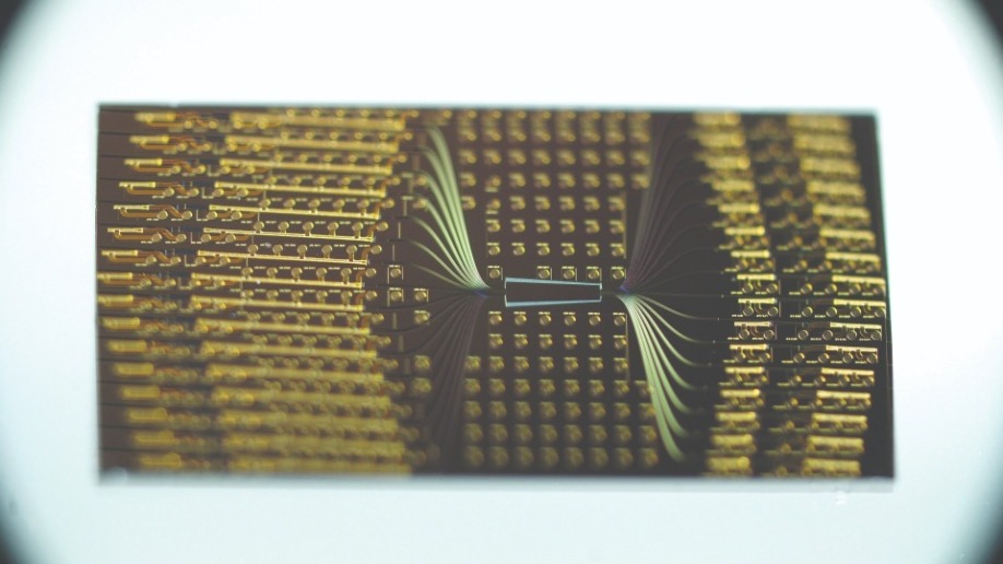
A die-level image of Ayar Labs prototype TeraPHY chiplet that includes all electronics and photonics I/O except the laser source.
Photonic integrated circuits (PICs) are the solution that data center managers crave: Smaller size. Less power. More capable. And like optical components in general, PICs are largely immune to the many interference sources that typically hamper purely electronic circuits.
PIC innovation comes in many forms, but for Ayar Labs – 2018 PIC Award corporate winners for photonic innovation – the solution came in rethinking how photonic and electronic circuits could be designed and manufactured. Using their approach, electro-photonic circuits can not only coexist in the same package, but be improved dramatically compared to today’s electronic devices that are limited by their reliance on wires and bonds.
PIC Magazine Technical Editor, Mark Andrews, met with Ayar Labs co-founder, Mark Wade, and the company’s CEO, Charlie Wuischpard to discuss the road that Ayar has taken and where the company is headed. Wade explained that the genesis of Ayar’s product line, which is now focused on emerging optical I/O applications, began back in the mid-2000s at MIT as part of the Defense Advanced Research Project Agency’s (DARPA’s) Photonically Optimized Embedded Microprocessors (POEM) project – the company was founded in 2015 based upon this research. Since Ayar Labs emerged from stealth mode into the early stages of product marketing, capitalization, and pilot line development, the journey has been long but rewarding. Ayar Labs announced in November 2018 that it secured (USD) $24 million in Series A financing from the likes of Playground Global, Founders Fund, Global Foundries and Intel Capital, just to name a few of the most well-known members of its continuing and new financial backers.
“Ayar Labs was formed in 2015 on the insights that electrical I/O was not going to keep up with industry demands as we go into the future. Secondly, that the traditional optical transceiver industry was not going to solve the problem that the electrical community and ASIC makers were facing. We focus on hybrid technology. This involves some new component and I/O architecture. The last year has been about further technology refinements – we are on our ninth tape-out – getting the financing in place and gathering specific customer requirements. So if we look back at where we were at PIC 2018, (April) we were getting indications that 2018 would be a big year for us because our value proposition was really starting to connect with some of the big players in the industry, and the fact that those players were facing the reality that electrical connectivity was not going to scale into the future,” Wade remarked.
Wade explained key differentiators in Ayar’s new approach to PIC hybridization by noting that current electronic–photonic chips are limited to niche manufacturing processes and include only a few optical devices alongside simple circuits. The Ayar approach is focused around an electronic–photonic system on a single chip integrating millions of transistors and hundreds photonic components that work together to provide logic, memory, and interconnect functions. This approach was previously used to build a microprocessor that uses on-chip photonic devices to directly communicate with other chips using light.
To integrate electronics and photonics at the scale of a microprocessor chip, the company adopts a ‘zero-change’ approach to the integration of photonics. Instead of developing a custom process to enable the fabrication of photonics, which would complicate or eliminate the possibility of integration with state-of-the-art transistors at large scale and at high yield, Ayar designs optical devices using a standard microelectronics foundry process typically utilized for modern microprocessors.
Ayar’s core technology – now backed by more than 25 academic papers – has been a decade in the making. “We focus on a new hybrid technology; this involves some new component and I/O architecture … So if we look back at where we were at PIC 2018, we had indications that some of the photonics industry’s biggest players were starting to take notice of the value that we could deliver – that has only grown since April. Those players were facing the reality that electrical connectivity was not going to scale into the future, and Ayar Labs offered an appealing solution,” Wade remarked.
“We have already built standalone demonstrators – our first public demonstration was at OFC this year. When we demonstrated the technology working at full capacity, it generated a lot of inbound interest from those who are not traditionally component people. That led to the project that we are involved in now, and we are seeing a proliferation of players looking at the same sort of problems – the plan is to co-design and co-develop these types of solutions in the next year and then introduce them into some new systems the following year,” he added.
A die-level image of Ayar Labs prototype SuperNova, the company’s laser power supply that can provide energy for up to 6.4 T/bps aggregate bandwidth.
“People have been embarking on some various technologies that (address) these needs, and they are not working all that well, while (designers and customers) are finding that original design ideas are more problematic than they thought – But we have to show and demonstrate a successful solution and people are starting to recognize that (Ayar’s designs) are a good solution; there is a lot of interest in this since other approaches are not working all that well,” said Charlie Wuischpard. Before taking over leadership at Ayar Labs, he said much of his experience at IBM and Intel had the effect of leading him to the right place at the right time.
“No matter what I did, the key need was connectivity and as we (at Intel) were exploring new system architectures, we always wanted to help Moore’s Law to continue scaling. But from a cost-effective basis it was and is failing, which is the reason behind the new looks at system architectures so many companies are taking… Ultimately, the challenge comes down to moving data more quickly between the points; networking and connectivity have become key issues for industry, which is where the Ayar Labs solution fits …. When I was first introduced to Ayar Labs this summer, I saw the world is heading to improve density, reduce latency and reduce power consumption – a long list of benefits that are possible ... the lightbulb went off for me that Ayar delivers the right technology at the right point in time. Because of the long design cycle that we are working with now, you’ll start seeing products showing up in 2020 and 2021,” he added.
As the company has completed its first major funding round, work continues on device level development along with a push for standardization that the company believes will benefit not only their own work, but that of PIC manufacturers working across applications. If PICs are to replace or at minimum augment existing pluggable transceiver technologies, standardization of electronic/photonic connections as well as a move towards automated TAP are essential.
“There is strong support for Ayar Labs approach from our investors: Playground Global, Intel, Global Foundries and others. We will make a steady stream of announcements over the next year; we’ll see more in the spring, summer and winter. The efforts that we will join and participate in with regard to standards will be a big piece of our work going forward,” Wuischpard concluded.
The 2019 PIC International Conference is the place to gain an insiders perspective from leading companies and associations driving advances in photonic integration. PIC International is colocated with Compound Semiconductor International and Sensor Solutions International, 26-27 March 2019 in Brussels, Belgium.
Visit the conference website at https://picinternational.net for more information or to reserve your space today.
Fraunhofer HHI has advanced its hybrid PolyBoard platform for PIC designs through its micro-optical bench concept. PolyBoard enables the first steps towards 3D photonic integration with ultra-widely tunable lasers for emerging applications such as life sciences, LIDAR, and quantum technologies.
By Martin Schell, Director, Fraunhofer Heinrich Hertz Institute
HHI’s hybrid photonic technology PolyBoard allows for a broad spectrum of applications, ranging from the traditionally photonic telecom/datacom fields, to life sciences and the emerging quantum technologies. The PolyBoard PICs rely on a polymer-based waveguiding platform, and in the past years, numerous optical building blocks such as 90° hybrids, AWGs, thin-film-based wavelength filters and polarization handling elements, variable optical attenuators, and optical switches have been made available [1],[2].
Actives such as laser diodes, gain chips and photo diodes can be integrated into the PolyBoards by means of end-fire coupling or micro-machined 45° mirrors. Additionally, on-chip coupling features, U-grooves, enable adjustment-free attachment of fibers, simplifying enormously the effort and lastly cost of photonic packaging. Most recently, three new developments in the PolyBoard technology have enabled new ways of approaching photonic integration to fulfill the demands of ever increasing complexity of PICs: an on-chip micro-optical bench, ultra-widely tunable lasers, and the capability for 3D photonic integration. In this article, these three new developments are reviewed, and a vision on their impact in different application fields is provided.
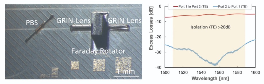
Figure 1 (left) Integrated optical isolator consisting of a polarization beam splitter (PBS), a Faraday rotator and half wave plate integrated via two GRIN-lenses. (right) Measurement results showing an optical isolation larger than 20 dB across the C-band.
PolyBoard micro-optical bench
One of the most challenging components to implement into today’s PICs are optical isolators and circulators. All published attempts for optical isolation are still far from reaching a performance attractive enough for their integration in PICs. On the other hand, micro-optical free-space based optical isolators, extensively used in packaged photonics, show low insertion and return losses as well as high optical isolation.
At ECOC 2018, HHI demonstrated a first PolyBoard integrated optical isolator consisting of an on-chip free-space section with GRIN-lenses for beam collimation [3]. The GRIN-lenses are inserted into pre-etched U-grooves, normally used for single mode fiber coupling, which enable passive alignment of the lenses and the polymer waveguides. This free-space section allows for the insertion of optical bulk materials such as Faraday rotators, which are one of the key components for the fabrication of optical isolators, or even complete miniaturized optical free-space isolators consisting of a 45° Faraday rotator and two polarization filters.
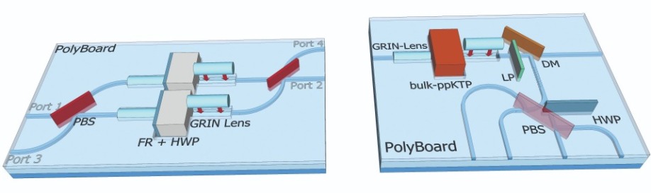
Figure 2. Concept of a PolyBoard integrated polarization independent circulator (left). Concept of an entangled photon source for quantum applications using a Potassium Titanyl Phosphate (KTP) crystal (right).
On-chip losses below 0.5 dB for chip integrated free-space sections have already been demonstrated, paving the way to PolyBoard based optical isolators with losses below 1.0 dB [4]. The integration of external Faraday rotators into the PolyBoard also enables the realization of optical circulators, targeting applications not only in telecommunications but also in life sciences, such as fiber based interferometer structures in optical coherence tomography (OCT). The concept for a PolyBoard enabled optical circulator is shown in Figure 2 (left).
Beyond the implementation of isolators and circulators, it is possible to use the Micro-Optical bench to integrate crystals such as Potassium Titanyl Phosphate (KTP) or Lithium Niobate (LiNbO3). This will allow the novel inclusion of nonlinear optical effects like spontaneous parametric down-conversion (SPDC) on PICs. These nonlinear crystals are envisioned to be key elements in the generation of entangled photon sources required for quantum communication (see Figure 2, right). This approach is currently being developed in the European flagship project UNIQORN, which started in October 2018. Together with 16 other consortium partners HHI takes a leading role in the development of PICs for applications in quantum technology like quantum key distribution (QKD) or quantum random number generators (QRNG). The PolyBoard Micro-Optical Bench allows for the integration of virtually every thinkable material and thus represents one of the unique features of the PolyBoard integration platform.
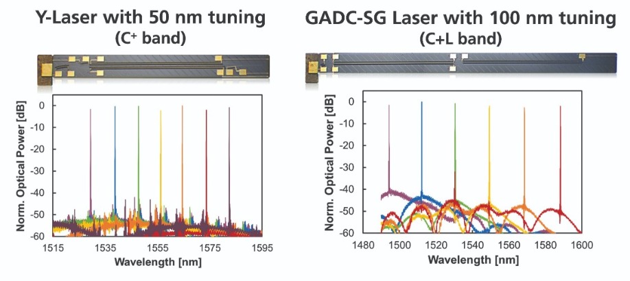
Figure 3. New PolyBoard-based ultra-widely tunable lasers. A first implementation (left), namely Y-laser, is based on the Vernier-effect to enhance the tuning range. Two sampled-gratings (SGs) act as comb reflectors with different periodicities. A tuning range of 50 nm along the C-band has been recently demonstrated. A second implementation, based on a SG periodic comb reflector and a grating-assisted directional coupler (GADC) as an intra cavity filter, has demonstrated tuning ranges of up to 100 nm. These two tunable lasers open the door towards ultra-broadband PolyBoard-based DWDM PICs in telecom/datacom applications.
Polymer materials can be used for the implementation of highly efficient thermo-optically tunable structures.
This allows for the development of III-V/polymer tunable DBR lasers with 20 nm tuning range along the C-band and, depending on the application, direct modulation capabilities of 10 Gb/s, output powers up to 40 mW, or linewidths narrower than 200 kHz.
Due to the thermal tuning, however, tuning ranges above 20 nm are not possible by simply heating a polymer Bragg grating. During the ECOC 2018 in Rome, this limit was overcome with two new III-V/polymer implementations, (see Figure 3) [5]. A first implementation, namely Y-laser, is based on the Vernier-effect to enhance the tuning range. Two sampled-gratings (SGs) act as comb reflectors with different periodicities. This increases the tuning range to 50 nm. Furthermore, a second implementation, based on a SG periodic comb reflector and a grating-assisted directional coupler (GADC) as a ultra-widely tunable intra cavity filter (GADC-SG) - has demonstrated tuning ranges of up to 100 nm. These new tunable laser devices open the door towards PolyBoard-based ultra-broadband DWDM PICs in telecom/datacom applications. A taste of the level of optical functionality that can be potentially implemented using the PolyBoard technology with these new laser types is shown in Figure 4, where a hybrid PIC comprising a tunable laser combined with Micro-Optical bench functionalities such as an optical isolator and an etalon-based wavelength monitor are presented.
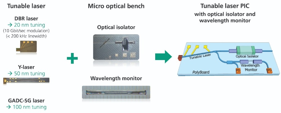
Figure 4. Concept of a PolyBoard PIC comprising already demonstrated optical building blocks such as tunable lasers, optical isolators, and wavelength monitors. This example shows the level of functionality that the PolyBoard technology can provide to PIC integration.
PolyBoard 3D photonic integration
The 3D photonic integration opens a new disruptive way for designing photonic integrated circuits. The possibility of a multilayer waveguide system to enable 3D photonic integration adds a new degree of freedom to PICs [1]. This newfound flexibility leads to novel applications like space division multiplexing (SDM), optical phased arrays for LIDAR, or large-scale crossing-free switching matrices. The latter has been demonstrated in 2D PICs [6], but due to the planar matrix design in large-scale switching matrices a large number of waveguide crossings occur, adding additional losses and channel crosstalk to the system (Figure 5, left). By entering the third dimension, most of these waveguide crossings can be avoided, leading to reduced on-chip losses and crosstalk (Figure 5, right).
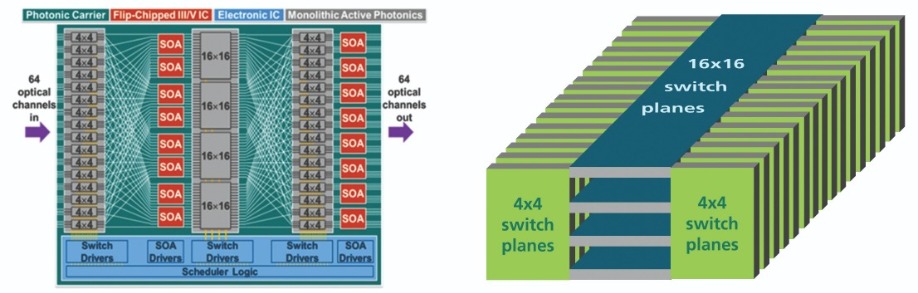
Figure 5. Schematics of a 64x64 switching matrix in a) two-dimensional structure [7] and b) three-dimensional structure.
The right side of Figure 6 shows that losses as low as 1.0 dB for the TE and 0.9 dB for the TM polarization at a wavelength of 1557 nm can be achieved.
Within the EU-H2020 Project 3PEAT, complex hybrid 3D PICs for LIDAR and miniaturized vibrometers are being developed combining the 3D photonic integration features of HHI’s PolyBoard and optical beam forming networks in LioniX’s TriPleX technology (Figure 7, left). Furthermore, 3D photonic integration is also being used in a 3D crossing-free switching matrix for top of rack switches in data centers (Figure 7, right).

Figure 6. 3D sketch of a vertical MMI coupler for a vertical centre-to-centre distance of 7.2 µm with simulated results for the optical light field (left). Results from the fiber-chip-fiber measurement of a fabricated VMC for TE and TM polarization. The fabricated device has a length of 173 µm and a width of 1.4 µm. The marked line corresponds to the simulated minimum loss for a VMC width of 1.4 µm and a wavelength of 1550 nm (right).
The PolyBoard Micro Optical bench, the PolyBoard Ultra-Widely Tunable lasers, and the first steps into the third dimension, together with the transparency of polymers from the NIR down to the visible (VIS) range, allows for the implementation of completely new classes of PICs over a broad spectrum of wavelengths.
These developments position the PolyBoard platform as an enabling photonic integration technology in emerging application fields such as life sciences, LIDAR, and quantum technologies.

Figure 7. Schematic layout of a PolyBoard/TriPleX based laser Doppler Vibrometer module (left), schematic 4 x 4 switching module consisting of four PolyBoard waveguiding layers (right)
References
[1] D. de Felipe et al., “Recent Developments in Polymer-Based Photonic Components for Disruptive Capacity
Upgrade in Data Centers”, J. of Lightwave Technology, Vol. 35, No. 4, p. 683 (2017).
[2] M. Kleinert et al., “Photonic integrated devices and functions on hybrid polymer platform”, Photonics West,
10098-45, 2018.
[3] H. Conradi et al., “High Isolation Optical Isolator: A new Building Block for PolyBoard Photonic Integrated
Circuits”, We4C.3, ECOC (2018).
[4] M. Happach et al., “On-chip free beam optics on a polymer-based photonic integration platform”,
Vol. 25 No. 22, Optics Express (2017).
[5] D. de Felipe et al., “Ultra-Wide Band Tunable Lasers on the PolyBoard Polymer-Waveguide Based Photonic
Integration Platform”, We4C.3, ECOC (2018)
[6] L. Schares et al., “Etched-facet semiconductor optical amplifiers for gain-integrated photonic switch
fabrics”, ECOC 2015, Valencia.
[7] M. Nuck et al., “Low-loss Vertical MMI Coupler for 3D Photonic Integration”, Tu4C.6, ECOC (2018).
EPIC is the industry association that promotes the sustainable development of organisations working in the field of photonics in Europe...

26-27 March 2019 Brussels, Belgium PIC International provides comprehensive coverage of every key sector within the integrated photonic circuits industry...
POET Technologies is a global provider of innovative photonics products and services...
POET Technologies is a global provider of innovative photonics products and services...

VLC Photonics is an independent provider of photonic integration solutions, offering services such as: optical integration consulting, photonic circuit design, in-house chip characterization, and brokerage for fabrication and packaging...
IQE is the leading global supplier of advanced semiconductor wafer products that cover a diverse range of applications...

Well known for the high quality of its products, PI (Physik Instrumente) has been one of the leading players in the global market for precision positioning technology for many years...

PHIX’ ambition is to become the world’s first automated photonics assembly and packaging line for medium and large volume photonic integrated circuits (PICs), photonic components, assemblies and modules...

Tipps is a specialized solution provider for PIC (Photonic Integrated Circuits) evaluation & packaging by supplying dedicated and mid-range volume packaging services...
Compound Semiconductor Magazine provides the latest news, features and analysis within the compound related industry sector...

The ECOC Exhibition is the largest optical communications exhibition in Europe, held each September in a different European city, the event is the key meeting place for decision makers from across the fibre optic communications technology industry...
On October 2, 2018, the 4th edition of the Photonic Integration Conference will take place at High Tech Campus Eindhoven, The Netherlands, during the Photonics Applications Week [Sep 30 – Oct 05, 2018, https://phappsweek...
Silicon Semiconductor magazine publish news and technical features on the silicon semiconductor industry, about semiconductor manufacturing, lithography, semiconductor equipment manufacturers, EUV, 450nm and 32nm requirements...

Lumerical develops photonic simulation software – tools which enable product designers to understand light, and predict how it behaves within complex structures, circuits, and systems...

Synopsys is driving the photonic integrated circuit (PIC) revolution with design automation solutions for applications ranging from data communications to sensors and biomedical devices...

VPIphotonics™ sets the industry standard for end-to-end photonic design automation comprising design, analysis and optimization of components, systems and networks...
Twelve months in our buyer's guide, covering the complete integrated circuits value chain giving you:
Join buyers guide here: https://picmagazine.net/join-buyers-guide

