
When I first heard of using CPV to power satellites, I thought it rather odd. But now, having learnt more about it, I’m starting to come around to the idea.
Up in space, this technology would take the form of modules incorporating from small cells and lenses. Modules would be pointed at the sun with high accuracy, just like the panels on the satellites of today.
Due to the high costs of getting anything into orbit – launch costs are around $10,000 per kilogram – key figures of merit for generating power in space are watts-per-kilogram and
watts-per-cubic metre.
Judged in those terms, CPV has great potential. Moving from flat panels to high concentration delivers a significant boost in efficiency, and by using lens with a focal length of just a few millimetres, the modules can be incredibly thin. So thin, in fact, that they can be drop-in replacements for conventional satellite panels.
Additional advantages of this class of module are a very high radiation tolerance, thanks to shielding from a glass lens array; and a reduced risk of arcing between cells, because these devices are spaced far apart.
Putting this concept to the test is a team from George Washington University, the US Naval Research Labs, Veeco, Northwestern University, MIT and X-Celeprint. This collaboration is developing modules that feature an array of small lenses, positioned above five-junction cells formed via the heterogeneous integration of triple-junction GaAs-based cells with dual-junction, InP-based cells. The modules can also capture diffuse light, thanks to the inclusion of a bifacial crystalline solar panel (see Sending CPV into space on p.36 for details).
Commercial success with this technology could be a double-edged sword for our industry. By increasing the bang-per-buck of solar power, it could lead to the launch of more satellites; but the III-V content on each one would be far, far lower.
The flip-side, however, could be growth in the CPV industry. Ultimately, this technology could then have more success back on earth.
It is well known that CPV failed to deliver its commercial promise in sunny climes, due to plummeting prices for silicon and the credit crunch. But the question marks surrounding its long-term reliability can now largely be dismissed, thanks to the efforts over the last decade at ISFOC (see Putting CPV to the test on p.28). So, as the levelised cost-of-energy falls, could CPV be poised to make a comeback?
The materials and optoelectronics firm II-VI and the optical communications company Finisar have entered into a merger agreement under which II-VI will acquire Finisar in a cash and stock transaction with an equity value of approximately $3.2 billion. I-VI and Finisar will employ over 24,000 associates in 70 locations worldwide upon closing the transaction.
The combination of II-VI and Finisar brings together their extensive capabilities in photonics and compound semiconductors to serve a number of fast growing markets including communications, consumer electronics, military, industrial processing lasers, automotive semiconductor equipment and life sciences.
The joint portfolio includes GaAs, InP, SiC, GaN and diamond technologies together with optoelectronic, optical and integrated circuit device design expertise and related intellectual property. This has the potential to unlock access to larger markets in RF devices for next-generation wireless and military applications, as well as power electronics for electric cars and green energy.
The combined company also has a full line and scalable supply of high performance datacom transceivers, products based on coherent transmission technology and ROADM solutions. It will market products into next-generation undersea, long-haul and metro networks, hyperscale datacentres and in 5G optical infrastructure.
There is also huge potential in 3D sensing and LiDAR based on their optoelectronics expertise in GaAs and InP compound semiconductor laser design platforms, together with one of the world's largest 6-inch vertically integrated epitaxial growth and device fabrication manufacturing platforms.
"Disruptive megatrends driven by innovative uses of lasers and other engineered materials present huge growth opportunities for both of our companies," said Vincent D. Mattera, Jr., president and CEO, II-VI Incorporated. "In communications, materials processing, consumer electronics and automotive, we expect that the combination with Finisar will allow us to leverage our combined technology and intellectual property in InP, GaAs, SiC, GaN, SiP and diamond to achieve faster time to market, cost and scale. Together, we believe that we will be better strategically positioned to play a strong leadership role in the emerging markets of 5G, 3D sensing, cloud computing, electric and autonomous vehicles, and advanced microelectronics manufacturing."
Mattera continued: "We have long admired Finisar and have a great deal of regard for its founders and its talented global team. Our companies both have a long history of focusing on innovation, breakthrough solutions and competitive follow-through by manufacturing high quality products for our customers, and we look forward to welcoming Finisar to the II-VI family and further strengthening our competitive position in the industry."
"The combination of our state-of-the-art technology platforms, deep customer relationships, great assets and amazing talent will enhance our ability to hit market windows that won't stay open for long," said Michael Hurlston, Finisar's CEO. "This combination will accelerate our collective growth and will take advantage of the technology, products and manufacturing expertise that Finisar has uniquely developed over the course of its 30 year history."
Hurlston added, "We are extremely excited to combine Finisar with II-VI and together create a leader in photonics and compound semiconductors across all of the markets we serve. We are confident that the growth potential for the combined company is substantial, and we believe that our respective shareholders will be able to enjoy significant potential for value creation when the transaction is completed."
A UK and Netherlands consortium of semiconductor device specialists has been awarded a two year, £1.2Million project to develop next generation photodetector solutions for ultra-high speed data-communications applications.
The Compound Semiconductor Centre (CSC) will deliver project MISCA (Monolithically Integrated Detector Solutions for Next Generation Communications Applications) in collaboration with Integrated Compound Semiconductors (ICS) Ltd of Manchester, and VTEC Lasers and Sensors of Eindhoven, The Netherlands.
Project lead, Wyn Meredith, director of CSC, commented: "The project aims to drive a radical improvement in component performance via advances in semiconductor materials integration and will result in a new European source of high performance detector products for fibre optic data-communications applications."
Mohamed Missous, founder and CEO of ICS said: "The rapid growth of the high speed optical transceiver market is an exciting opportunity for ICS as the demands of the 100G/200G/400G optical transmission markets require a deep understanding of RF component design to complement high quality optoelectronic device manufacture."
Jan Mink, CEO of VTEC added: "The Eurostars programme is specifically aimed at enabling agile SMEs to collaborate across Europe, and gives VTEC a great opportunity to collaborate with like-minded companies in the UK to extend our value chain. We see great potential in using semiconductor component integration to enable a new class of low power consumption, high performance detector products."
After a relatively flat year in 2016, revenue in the RF GaAs device market grew by more than 7 percent in 2017. While a wide variety of commercial and defence applications use GaAs devices, the wireless market continues to be the dominant user of this technology.
Mobile handsets will continue to define the revenue trajectory, but emerging 5G network deployments will contribute to future growth. The Strategy Analytics Advanced Semiconductor Applications (ASA) service report, 'RF GaAs Device Industry Forecast: 2017 - 2022' forecasts that RF GaAs revenues will push past the $9 billion milestone by the end of the forecast timeframe.
The Strategy Analytics Advanced Semiconductor Applications (ASA) service report, "RF GaAs Device Industry Forecast: 2017 - 2022," forecasts that RF GaAs revenues will push past the $9 billion milestone by the end of the forecast timeframe.
"Despite the dominance of the wireless segment, the RF GaAs market has been notable for the breadth of applications using the technology," noted Eric Higham, service director, Advanced Semiconductor Applications (ASA) service. "However, GaAs devices are facing challenges from other technologies and they are being commoditised in many of these applications. Future growth is going to depend heavily on LTE and emerging 5G networks."
"The situation for RF GaAs growth in the defense market is different," observed Asif Anwar, director of the Advanced Defence Systems (ADS) service. "New defence platforms and major upgrades are reaching the production phase and while the radar segment will remain the dominant application, all the defence segments will experience growth."3-5 Power Electronics, GmbH (35PE), an emerging power semiconductor technology innovator, has announced that it has secured new financing from the Sturm Family Office (SFO) of Bad-Mergentheim in Germany.
35PE has pioneered a first-of-a-kind process to deposit thick GaAs layers on top of GaAs substrates to produce high-voltage/high-current power semiconductors. The process aims to produce superior power devices at a lower manufacturing cost than devices built with silicon or SiC. Near-term applications include industrial motor drives, uninterruptible power supplies, and renewable energy products, such as wireless chargers for solar and wind inverters. Future applications include electric vehicles, robotics and 5G technologies.
35PE was founded in late 2015 to optimise GaAs technology to enable power devices. Led by a team of semiconductor technology and global business executives, the company has raised 5.3 million euro (US$6.10 million) to date. This includes funds previously secured from Shanghai-based SINO Alliance Investment Ltd. The new funds will be used to prepare 35PE's operations for product commercialisation which is planned for the second half of 2019, and to forge partnerships with established leaders to help speed the company's GaAs devices to market.
Samples of the company's GaAs diodes have been submitted for testing to power module makers in Europe and China. Applications include battery charging, welding and industrial heating.
GaAs technology has been used for decades to produce low-voltage/high-frequency devices. Now, the industry is leveraging the technology to build compact high-power semiconductor devices because of its inherent advantages over silicon, SiC, GaN, and other materials. Devices based on GaAs technology deliver higher energy savings, superior performance and greater reliability than those based on silicon.
For instance, when compared to a conventional SiC Schottky diode in a 3.3 kW wireless charging system, a GaAs-based device was shown to consume nearly 20 percent less power. What's more, GaAs-based power modules and systems can be as much as 50 percent smaller and lighter than the silicon alternative. Also, when compared to devices fabricated with wide-band gap (WBG), SiC and GaN materials, GaAs-based devices are far less costly to manufacture, while demonstrating equal, and often better performance advantages.
35PE's vision was to stretch the capabilities of GaAs technology and simultaneously improve the manufacturing economics. Thick GaAs layers are imperative for the production of high-power devices (>600 - 1700V and up to 100-150A). The company is the first in the industry to pioneer deposition technologies to produce high-power GaAs devices in high volume.
“We are thrilled to receive the new funding from SFO,” said 35PE's Chief Executive Officer, Dr. Gerhard Bolenz. “While we've laid the foundation to deliver a unique enabling technology solution to the power electronics industry, the new funding will help us build a global business. Most importantly, with growing customer interest in our technology, we can size our infrastructure for speedy response and service. We're grateful for SFO's support, and thankful to our existing investor who has championed our journey so far.”
SFO statement: “SFO is pleased to support 35PE with this new financing. We believe that the technology is clever, differentiated and enabling, with real potential to transform the power electronics industry. With nearly 90 years of collective semiconductor experience, the 35PE team has achieved critical technology milestones by executing with focus and discipline, and using their resources wisely.
At its headquarters in Dresden's Silicon Saxony region, 35PE has established a lean model to develop, produce and distribute high-voltage GaAs wafers and related semiconductor devices for power electronics. Multiple patents have been filed worldwide and one has already been granted. In addition, the company has established select distribution networks in Asia to create an efficient feedback loop between the company and end-users. In parallel, the company is pursuing partnerships with strategic investors and global manufacturers to execute more speedily on its technology roadmap and accelerate its market entry.
Infineon has acquired Siltectra, a Dresden-based start-up that has developed an innovative technology called Cold Split to process crystal material efficiently and with minimal loss of material. A purchase price of €124 million was agreed on with the venture capital investor MIG Fonds, the main shareholder.
Infineon will use the Cold Split technology to split SiC wafers and double the number of chips per wafer.
"This acquisition will help us expand our excellent portfolio with the new material SiC as well. Our system understanding and our unique know how on thin wafer technology will be ideally complemented by the Cold Split technology and the innovative capacity of Siltectra," said Reinhard Ploss, CEO of Infineon. "Thanks to the Cold Split technology, the higher number of SiC wafers will make the ramp-up of our SiC products much easier, especially regarding further expansion of renewable energies and the increasing adaptation of SiC for use in the drive train of electrical vehicles."
Jan Richter, CTO of Siltectra: "We are glad to become part of the team of the global market leader in power semiconductors. Having shown that the Cold Split technology can be used at Infineon in principle, we will now work together to transfer it to volume production."
Michael Motschmann, general partner of MIG Fonds' administrator MIG AG, said: "Since we invested in Siltectra more than eight years ago, we have always believed in the Cold Split technology and the great team. We are very pleased that we found Infineon as a buyer who fits perfectly technologically as well as culturally to the company. Furthermore, it makes us proud that we helped to strengthen Germany's economic competitiveness by our investment."
Siltectra was founded in 2010 and has been growing an IP portfolio with more than 50 patent families. The start-up developed a technology for splitting crystalline materials with minimal loss of material compared to common sawing technologies. This technology can also be applied with the semiconductor material SiC, for which rapidly rising demand is expected in the coming years. SiC products are already used today in very efficient and compact solar inverters. In the future, SiC will play a more and more important role in electro-mobility. The Cold Split technology will be industrialised at the existing Siltectra site in Dresden and at the Infineon site in Villach, Austria. The transfer to volume production is expected to be completed within the next five years.
Rohm recently announced the development of a 1700V/250A rated SiC power module that provides the industry's highest level of reliability optimised for outdoor power generation systems, such as inverters for solar power and converters for industrial high-power supplies.
In recent years, due to its energy-saving benefits, SiC is seeing greater adoption in 1200V applications such as electric vehicles and industrial equipment. The trend towards higher power density has resulted in higher system voltages, increasing the demand for 1700V products. However, it has been difficult to achieve reliability, and so IGBTs are typically preferred for 1700V applications.
In response, Rohm was able to reach high reliability at 1700V, while maintaining the energy-saving performance of its popular 1200V products, achieving the first successful commercialisation of 1700V rated SiC power modules. The BSM250D17P2E004 uses new construction methods and coating materials to prevent dielectric breakdown and suppress increases in leakage current. As a result, high reliability is achieved that prevents dielectric breakdown even after 1,000 hours under high temperature high humidity bias testing (HV-H3TRB). This ensures high 1700V withstand voltage even under severe temperature and humidity environments.
By incorporating Rohm's SiC MOSFETs and SiC Schottky barrier diodes into the same module and optimising the internal structure, it has been possible to reduce ON resistance by 10 percent over other SiC products in its class. This translates to improved energy savings in any application.
Going forward, Rohm says it will continue to expand its lineup to ensure worry-free use by customers and work to increase demand by offering evaluation boards that allow easy testing and verification of the SiC modules.
From end-to-end and in just five years, the Compound Semiconductor Applications Catapult intends to have transformed the UK supply chain. Chief Executive, Stephen Doran, tells Rebecca Pool, how this will be done.
In August this year, the South Wales-based Compound Semiconductor Applications Catapult launched with an ambitious remit to accelerate UK economic growth in compound semiconductor-related industries.
Having received a hefty £51 million in government funds, the centre already employs some 23 staff and intends to soon create around 100 jobs internally, including engineering positions.
As the Catapult chief executive, Stephen Doran, puts it: “We are open for business, hiring and ramping up business and want to make a real difference to the UK supply chain... come work and collaborate with us and we can grow UK industry.”
Ask Doran about future Catapult plans and he is quick to point out the scale of the opportunity for UK-based compound semiconductor companies.
Analysts have estimated the global market for compound semiconductors is set to grow from a 2016 figure of $66 billion to more than $300 billion come 2030; three times the growth rate of silicon.
What’s more, recent analysis from Doran and colleagues indicates that in 2017, the global market had already increased to $74 billion.
Given these rapidly rising numbers, the impact of even a few percent increase in market share could be profound for any nation.
“The UK currently has around 9 percent of this market share and we need to maintain this share,” says Doran. “But if we can help the UK to increase this share by even just one, two or three percent, this would make a significant difference from an economic perspective.”
According to Doran, collaboration amongst existing UK companies is going to be critical to growing to market share. Catapult figures indicate that the UK already has more than 100 companies actively working with compound semiconductor devices.
Meanwhile, some 5,000 UK businesses – of which 90 percent are SMEs – are designing and making electronic components, devices and systems.
For its part, the Catapult has already been in contact with hundreds of businesses – including Anvil Semiconductors, Microsemi and IXYS UK Westcode – to develop its strategy. And the centre intends to work with more than 1000 business and help to create 1000 jobs come 2023.
But right now, a coherent supply chain does not exist. As the chief executive points out: “We have talked with SMEs and sometimes these companies ask us, ‘how can you help us to gain access to the tier one players’. Yet at the same time, tier one players say, ‘where is the supply chain across the UK’.”
To help to address this disconnect, the CSA Catapult is in the process of setting up an Innovation Centre, scheduled to open at the end of March 2019. “This centre is designed to be open and collaborative, so companies can overcome this barrier and get together,” points out Doran.
Crucially, the centre will also house a design studio, as well as laboratories and test facilities supported by simulation and modelling tools to get compound semiconductor development out of the lab and into industry.
“From our discussions, SMEs see access to expensive capital as well as the expertise to operate the capital as a key industrial barrier; the Innovation Centre will help here,” says Doran.
“Today industry is well advised in, for example, silicon modelling tools, but life becomes difficult in mixed-signal [devices] and even more difficult when you bring in compound semiconductors; so we are looking to make investments to improve models so more designs can come through.”
The Catapult is also intent on designing and manufacturing Evaluation Modules – using UK-sourced semiconductors where possible – to help companies prototype systems more quickly and cheaply.
The first modules will be for power electronics, radio frequency and microwave, and photonic applications. And as Doran highlights: “There’s a cost, cycle time and labour element to developing these, and it will easily cost half-a-million pounds to develop an evaluation module.”
“But we are in the process of deciding the first modules with industry now, as we want to get [devices] to the market fast,” he adds. “We expect to deliver six in the next two years.”
In addition to the Innovation Centre and Evaluation Modules, Challenge Programmes also form a critical, third arm of the Catapult’s strategy. Due to be announced within weeks, these programmes will be set up to identify how compound semiconductors can address global challenges and help SMEs to supply products to large companies with access to global markets.
As part of this, the Catapult will be assessing if industry needs a particular compound semiconductor supply chain, and has already identified the need for a scalable supply chain in the production of silicon carbide. “This doesn’t exist today as an open foundry,” says Doran. “If companies want to buy silicon carbide they go elsewhere or create that capability themselves.”
“But if we create a silicon carbide supply chain in the UK, and from there develop evaluation modules that go straight into industry, this would be a huge help... we would have a supply chain right on the doorstep for UK industry,” he adds.
Next moves
So as the Catapult makes its final decisions on Evaluation Modules and Challenge Programmes, bringing companies together to establish a solid UK compound semiconductor supply chain will no doubt remain a key theme. Doran is keen to highlight the successes of wafer producer, IQE, but also points out the potential to grow the supply chain from here.
“IQE are at the early part of the supply chain, yet more value lies at the consumer end of the chain,” he says. “So as we work our way along that supply chain, the more value we can embed in the UK, the better the overall economic impact for us.”
Indeed, only weeks ago, the Catapult announced a collaboration with the University of Bristol, to find out the best way to get the university’s cutting-edge thermal wafer mapping tool, Thermap, to the businesses that need to characterise wafers.
“The UK has so much core capability but we are not so good at collaborating,” he says. “We want to make sure companies in the UK understand the potential of what is in the UK... this ability to link one company with another is going to be extremely powerful.”
With rapidly rising revenues, industry can expect more growth and a ‘dream MBE’ system from Riber, reports Rebecca Pool.
For France-based semiconductor equipment business, Riber, 2018 has so far been very productive. Aided by buoyant market conditions, Riber’s revenue has grown 42 percent year-on-year for the first nine months of 2018, largely driven by sales of its MBE systems almost tripling.
And with analysts tipping the MBE system market to mushroom in coming years, Riber’s growth looks set to continue.
“Riber has always invested around 10 percent of its sales into research and development and we also have had a lot of collaboration with many European laboratories,” says Riber chief executive, Philippe Ley. “While research markets have been steady for many years, we are now seeing a lot of growth in production markets.”
“This is the era of IT and telecommunications, and MBE can produce very efficient devices for these markets,” he adds. “So for me, it is now all about improving existing equipment and developing new systems.”
Ley joined Riber in June this year, following an eight year stint as production and operations director as well as management board member. Tasked with driving company development as the MBE market grows, much has happened since he took the position of chief executive.
In July this year, Riber opened its 100 percent owned subsidiary, Riber Semiconductor Technology Shanghai, to strengthen the company’s presence across China.
As Ley points out: “Customers in China wanted better service, maintenance, help and after-sales service so this supports them, and provides the same service that you would get in Europe.”
Indeed, Riber already has 21 MBE customers in China with an installed base of 48 machines. Six of these are production systems, giving Riber the largest installed MBE base in China and a market share of more than 75 percent.
What’s more, in the same month, China-based laser systems developer, Acken Optoelectronics, ordered a MBE 6000 multi-wafer production system from Riber. And the company recently revealed a further sale to a ‘new customer from Asia’, to manufacture optoelectronic systems for fibre-optic interconnection markets.
Rising sales come at a time when several massive government projects are under negotiation to roll out large-scale fibre-to-the-home and 5G networks to serve Chinese markets.
“We know that Chinese customers would like to have more MBE systems in China so they can make more of their own electronic components, rather than buying them abroad,” says Ley. “People want fibre-to-the-home and 5G, and companies wish to be more independent... so yes, they will need more machines and our new subsidiary will be important.”
Looking beyond China, MBE system sales worldwide show an incredible 193 percent growth in the last nine months, compared with the same period in 2017. And Riber’s MBE systems order book is also looking very healthy, with orders increasing by a hefty 120 percent to €22.2 million in the last year.
According to the company, twelve systems – comprising seven production and five research machines – are scheduled for delivery between 2018 and 2019. In contrast, four production and two research systems were delivered in 2017.
Given this solid schedule, Riber predicts full-year revenues of Ä35 million for 2018 and at least 15 percent year-on-year growth. And Ley is confident the company will hit its targets, saying: “We have good prospects and a good plan and expect to see steady growth over the next three years.”
Dream machine
So what next for Riber? Right now, the company is intent on delivering what Ley calls its ‘dream MBE’ by 2021. As he explains, the next-generation MBE system will be ‘entirely user-friendly’ with a higher level of integration of in-situ characterisation tools, relative to current systems. Such tools will include optical-based flux monitors and pyrometers, and will provide the necessary deposition data to optimise quality control during epitaxy.
“You can sub-contract many of these tools, but we want to have an intelligent machine that can better use the system information to produce higher quality layers and better wafers,” says Ley. “It needs to be easy to use and have a high efficiency... we have many new customers around the world, and for sure in China, but not all have enough MBE knowledge.”
“Many customers do not want to make many tunings themselves, so such a system would really increase productivity,” he adds. “Our target is to develop a first system next year and have the final machine ready to be sold in 2021.”
But what about competition from MOCVD systems, perceived by many to be more user-friendly? Ley remains unfazed and as Riber chairman, Michel Picault, tells Compound Semiconductor: “MOCVD is a good tool for mass production while MBE is better for higher-end performance devices.”
“This is why we are seeing rising demand and potentially a very large market for these devices, including laser diodes and VCSELs, in 5G and fibre optic networks, and many more applications,” he adds.
As more and more wide bandgap semiconductors reach electric vehicle markets, industry can expect rapid power module package development, reports Rebecca Pool.
Earlier this year, Yole Développment analyst, Hong Lin, revealed how the in-flux of wide bandgap semiconductors to electric and hybrid electric vehicle markets is driving the development of new power-module packages.
As she tells Compound Semiconductor, more than twenty automotive companies are already using SiC Schottky barrier diodes or MOSFETs in DC-DC converters, the main inverter and onboard chargers, fuelling a 29 percent compound annual growth rate from 2017 to 2023.
What’s more, in the short-term, nearly all automotive manufacturers have programmes to implement SiC into the main inverter.
However, all good power devices need a good package to perform, and without a doubt, packaging has long been a bottleneck for wide bandgap device applications.
The packaging of SiC power devices has relied heavily on the same wire bonding approach used in silicon MOSFETs and IGBTs, largely because of its ease-of-use and low production costs.
But while this suits the tens-of-kilohertz switching frequencies demonstrated by silicon devices, hit the much higher megahertz speeds of SiC systems and parasitic inductances pose a problem.
Parasitic inductance in the power module induces high-voltage overshoot and ringing on switching devices, which then increases the device switching loss and EMI emission from the modules.
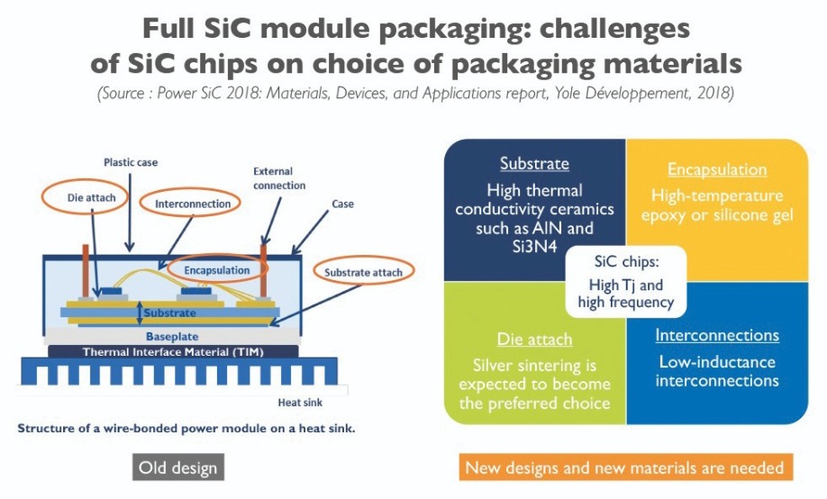
Couple this with the fact that the operating temperatures of SiC device packages now reach a scorching 225 °C, and one understands why the likes of Wolfspeed, Rohm, Infineon and GeneSiC have been busy pioneering new packaging structures to better handle the extreme switching speeds and temperatures.
At the same time, innovations, such as the use of copper connections and silver sintering joints instead of aluminium wire bonds and solder joints, have also emerged.
“Packaging-induced noise has a huge impact on device performance,” highlights Lin. “And so researchers have been working on reducing the inductance of the package, with many companies developing different types of packaging for this.”
The recent SiC-based inverter, developed by STMicroelectronics for Tesla’s all-electric Model 3, is a shining example of such innovation.
The inverter comprises 24 power modules, assembled on a custom-design ‘pin-fin’ heatsink. Each module contains two SiC MOSFETs with a novel die attach and connected directly onto the terminal with copper clips. Meanwhile a copper baseplate provides thermal dissipation.
“Tesla is one example, but almost all OEMs for car manufacturers have been looking at SiC technologies here, and each car company will adopt SiC at its own pace,” says Lin. “Mitsubishi Electric is another important player here, and has been providing lots of innovation in automotive as well as rail markets.”
Pick and choose
Still, automotive manufacturers remain technology-agnostic, keen to implement cost-effective, reliable systems, be they based on silicon or SiC.
“All silicon power device suppliers have a silicon carbide programme and are also looking at a gallium nitride programme,” comments Lin. “And there is not a packaging technology that we can say is only used in compound semiconductor-based systems.”
“These traditional silicon power device manufacturers also have a lot advantages over newer start-ups,” she adds. “For example, they understand packaging technologies very well and have a broad knowledge of applications and what a design needs... and of course they can leverage their internal capacity to take advantage of market growth.”
Indeed, looking to the future, Yole Developpment has forecast that the entire power module market will exceed $5.5 billion come 2023. “The industry is in an emerging stage right now with many companies proposing many different types of packaging,” says Lin. “The type of package also depends on its applications, and we can expect to see more and more customer designs being delivered to industry in the next few years.”
Wide bandgap semiconductors demand new package designs.
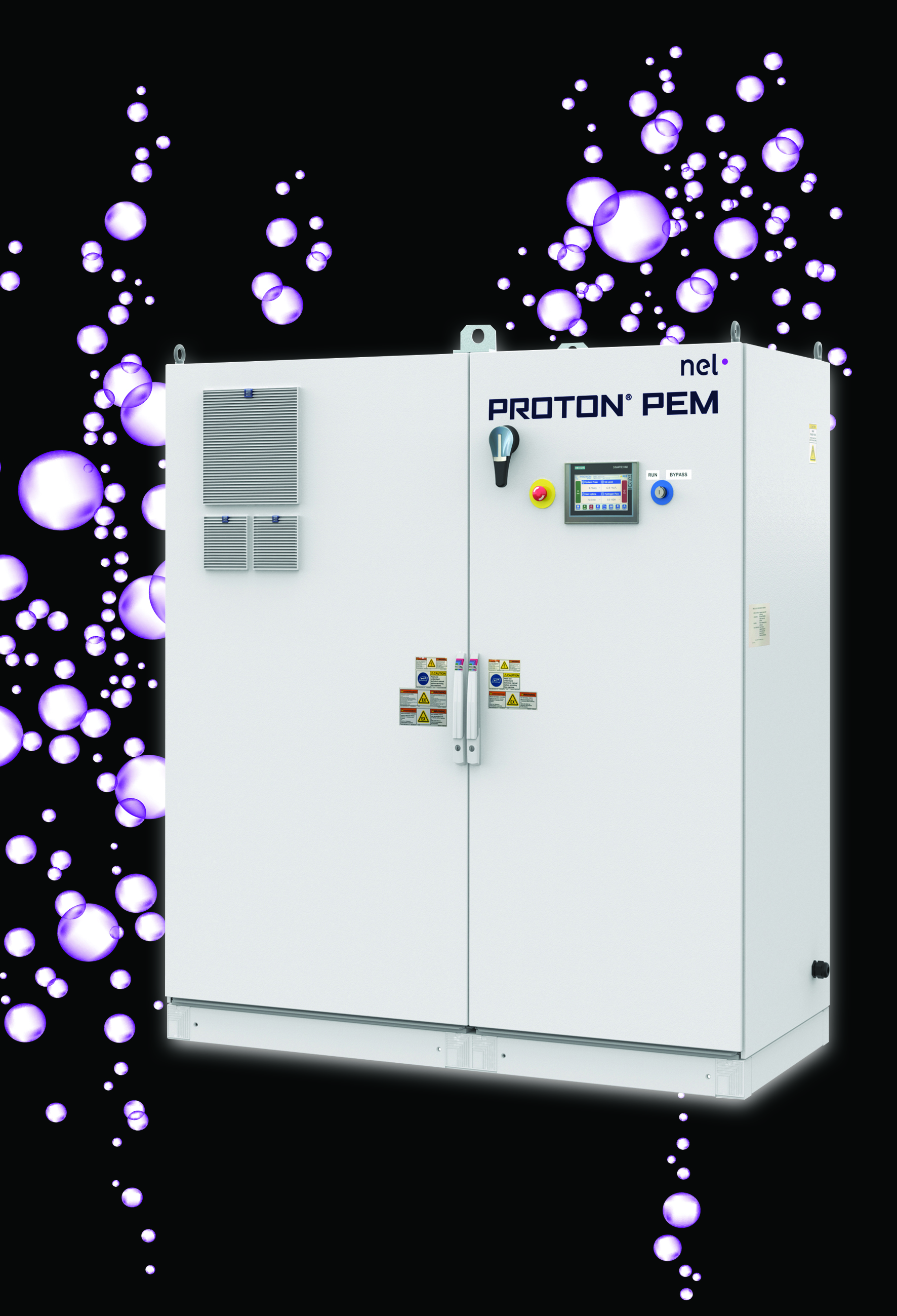
For low risk, low-cost production of high-purity hydrogen, makers of compound semiconductor epiwafers should install electrolysers based on proton exchange membrane technology
BY TOM SKOCZYLAS FROM NEL HYDROGEN
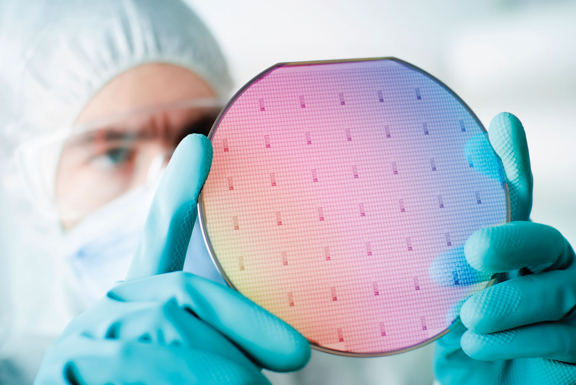
An essential process in the manufacture of compound semiconductor chips is the growth of a stack of epitaxial layers, which are subsequently processed into devices. Most often the growth of this heterostructure is carried out by MOCVD, a process that involves the decomposition of two or more types of organic molecule on a heated substrate to yield a thin film.
In this growth process, two key ingredients are metal-organics and the gases containing group V elements, such as arsine and phosphine – it is the decomposition of these sources and their subsequent reactions that produce the compound semiconductor epilayers. However, these are not the only materials with a critical role to play. There is also hydrogen, which is widely used in the production of devices based on arsenides and phosphides. This gas transports the metal organics, along with phosphine and arsine, from their containers to the growth chamber. Due to the rise in production of all forms of compound semiconductor chips, the demand for scalable, reliable, affordable, high-purity hydrogen is at an all-time high.
How pure is pure?
To ensure high-quality LEDs, VCSELs, transistors and the like, rigorous standards have been set for hydrogen purity. However, it is critical that this is assessed in a quantitative manner, rather than vague marketing terms. Different purity grades and terms are used by different suppliers, such as ultra-high purity and semiconductor grade – but they are just marketing nomenclature, and they fail to provide a quantitative description of the purity of the gas.
Makers of compound semiconductor devices will want to know the purity of hydrogen. It is often given in terms of the number of ‘nines’. For example, ‘five-nines’ would be used to describe hydrogen that is at least 99.999 percent pure. But that is not all that these chipmakers want to know. The nature of the impurity is also critical. It may be that the impurity is ‘destructive’ to the process, degrading process yield or impairing process control and leading to a cost increase in manufacturing. Or, worse still, impurities could result in device malfunction. That’s the threat with methane and CO, which may have to be completely avoided, or kept below well-determined limits.
Since the purity of hydrogen is so critical, it must be maintained up to the point of use. It is fruitless ensuring that the purchased hydrogen meets the level of purity for the process, and then compromising its integrity by transporting it to the facility through long-distance piping.
Delivery options
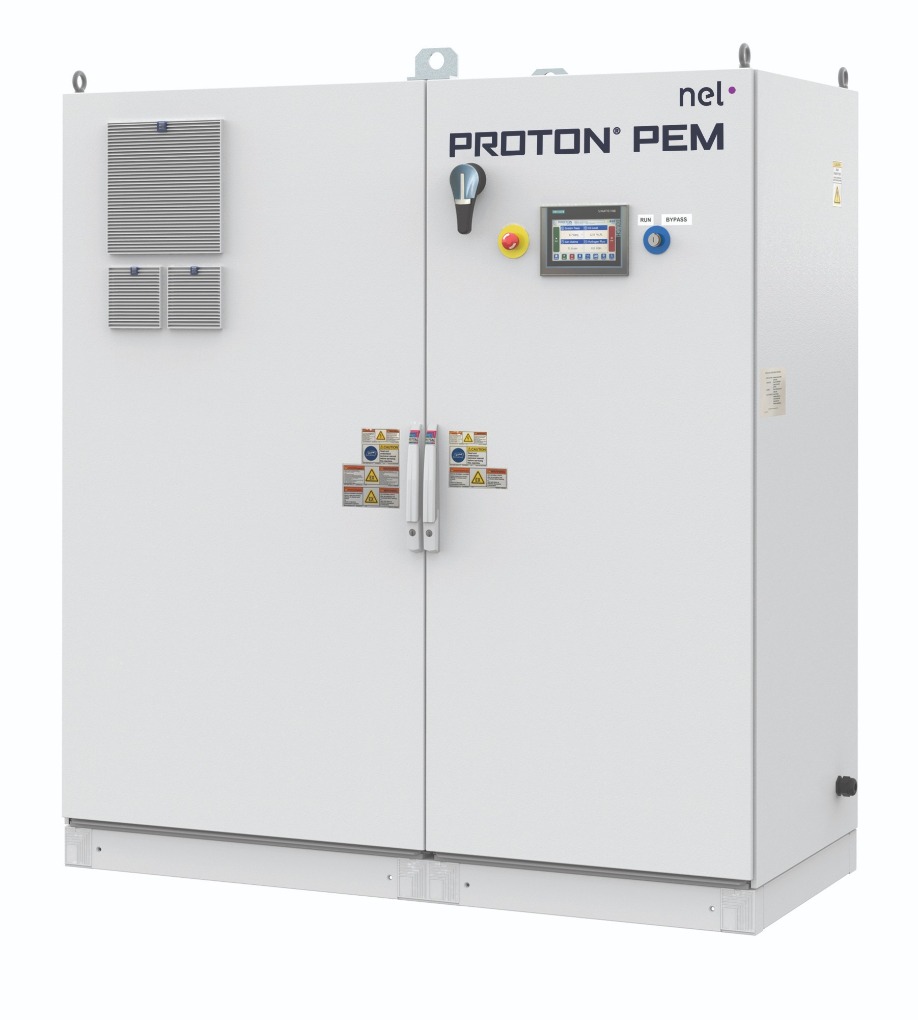
A pipeline is by no means the only option for delivering hydrogen. In fact, using a pipeline is rare, as it is only available when sites are near a large hydrogen production facility. More typical is delivery by truck. In that case, hydrogen either arrives in a compressed form in cylinders or high-pressure tubes; or for larger users, it is supplied as a liquid in a tank trailer, and offloaded into a site storage tank. There is also a third option, gaining in popularity: on-site generation using proton exchange membrane water electrolysers.
There are many challenges involved with delivered hydrogen, including specifying and maintaining purity. For instance, purity can be dependent on the method of production. Options for manufacturing hydrogen include methane or other hydrocarbon processing, salt brine electrolysis, and water electrolysis – and they can all introduce different impurities.
Once generated, all hydrogen is purified. How this is done is critical, depending on both what is removed and how this is accomplished. What are the risks to purity with this process?
Purity may be inconsistent, varying between batch deliveries. The cleanliness of the delivery vessels is beyond the customer’s control, as is the possibility of introducing contaminants every time a connection is made or broken on the supply side. Compromises to hydrogen purity can occur when filling up at the supplier’s facility, offloading at a previous stop or at the customer’s facility, or when changing out cylinders and tubes.
When deciding how to receive hydrogen, there are factors to consider that go beyond the integrity of purity. Delivery and offloading compressed gas or liquid hydrogen introduces site and personnel risk. There is also a safety risk associated with the moving, connecting and disconnecting of cylinders and tubes, and the transfer of liquid hydrogen from a tank trailer to a storage tank at the customer’s facility. All these tasks must be managed with strict discipline.
Many manufacturers of silicon wafer chip, semiconductor and MEMs use proton exchange membrane water electrolysers.
One drawback of having hydrogen delivered to a site is that its supply cannot be guaranteed. Deliveries can be delayed by a natural disaster, such as a storm or flood; by demand exceeding supply capabilities; and by labour strikes affecting the supplier’s plant or delivery methods. Whatever the reason, interruptions can wreak havoc. In the worst case scenario, chip making may have to stop, leading to the loss of key customers due to delays in shipments.
When hydrogen arrives on site, it needs to be stored with great care. It is a highly hazardous and flammable material, and it must be accommodated in tanks or cylinders that are compliant to codes and standards enforced locally and nationally.
In the US, storing of hydrogen must be undertaken in a way that meets precautions based on quantity and pressure, according to the NFPA2 Hydrogen Technologies Code, as well as codes prevalent in various states and municipalities. These codes may include EPA, NFPA, OSHA and frequently even more stringent local regulations.
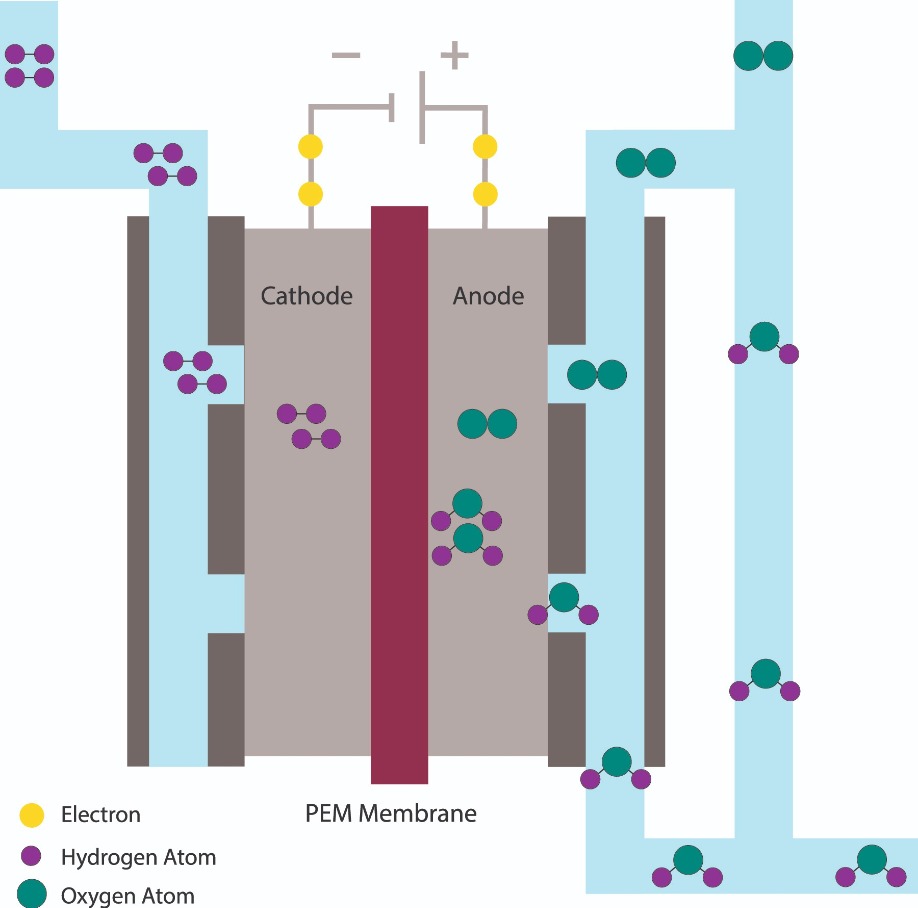
A proton exchange membrane water electrolyser cell stack produces hydrogen by splitting deionized water into hydrogen and oxygen. Unlike hydrogen produced from fossil fuels and other methods, there are no other contaminants present that can enter the hydrogen stream.
To meet these requirements, hydrogen storage may have to be sited well away from other buildings, in order to separate tanks from sources of ignition, air intakes, wiring, pathways and building walls. This situation brings its own issues, such as the need for expensive piping, which could become prone to leaks. There may also be the need for special permits, depending on local safety standards, that insist that engineering details are provided to appropriate authorities.
It is also important to be aware of the magnitude of the hazard. Just 1 m3 of hydrogen gas has a chemical energy equivalent to 2.9 kg of TNT. So a typical portable cylinder tank, which holds about 6.9 m3 of hydrogen, has as much energy as 20 kg of TNT – a sobering thought when manoeuvring hydrogen tanks and cylinders on or off manifolds feeding a facility. Note that typical facilities may store between 100 m3 and 3,000 m3 of hydrogen, equating to 290 kg to 8,700 kg of TNT. And if hydrogen is stored in liquid form, the magnitude of its energy is far, far higher. The remote possibility of a hydrogen explosion may not just be a major concern for those that work at the facility – it can be a worry for those that live nearby, who may over-estimate the risks and react in ways that do not support local chip making.
When siting a hydrogen storage area, several criteria must be considered. As hydrogen is not odorized, unlike natural gas, sensors and alarms may be required to alert safety personnel in the case of a leak. Storage may also need to comply with maximum inventory limitations according to regulatory codes, and there may be requirements for fencing and signage of the storage area. Generally, the sterile area near hydrogen storage is unavailable for parking or other uses.
On-site generation
An increasing number of compound semiconductor chipmakers are avoiding issues associated with the over-the-road delivery and storage of hydrogen by switching to on-site generation of hydrogen, in the form of proton exchange membrane (PEM) water electrolysers.
A key benefit of this technology is that it eliminates risks associated with deliveries and the maintaining of a hydrogen supply – because there is zero inventory required. Eliminating a hydrogen inventory means that the regulations associated with bulk hydrogen storage no longer apply. With a hydrogen generator, the magnitude of any leak cannot exceed the hydrogen production rate. Thanks to this, there is no danger of a leak filling the surrounding area with hazardous levels of hydrogen. What’s more, all piping remains tight, as there is no need to remove, replace or refill tanks.
When considering purchasing a PEM water electrolyser for on-site hydrogen generation, one should make sure the system is designed in accordance with NFPA and OSHA regulations for indoor installation. This means that the hydrogen supply can be closer to the point of use, trimming the length of piping, and in turn minimizing the risk of leaks and contamination.
With appropriate drying, PEM water electrolysers can produce pressurized hydrogen with a purity of at least 99.9995 percent on a constant basis, due to the stoichiometry of the generation process. Using this approach, production avoids the introduction of contaminants associated with the manufacture and transport of hydrogen from other sources, such as petroleum-based raw materials. The technology
also eliminates variations in impurities from batch to batch, because electrolysers continually produce hydrogen from water. In addition, contamination issues arising from cylinder change-out and refilling are eliminated.
Reliability also benefits from the use of electrolysers. As hydrogen is made on-site and on-demand, the supply of this source is not disrupted by uncontrollable situations such as severe weather, traffic tie-ups, accidents, labour strikes at the
supplier or trucking facility, and shortages in the supply chain. The generators are fully automatic, so no personnel are required for 24/7 operation (dependability is proven in submarines, where PEM electrolyser cell stacks provide oxygen for life support). Since there are limited moving parts – primarily a circulation pump, a circulation fan and a few solenoid valves – these units require minimal maintenance.
PEM water electrolysers also have the upper hand in terms of cost control. The price for hydrogen delivered from an off-site source may fluctuate significantly, while the costs for hydrogen generated on-site with an electrolyser are relatively fixed, and limited to capital, electricity and preventive maintenance.
Another benefit of PEM water electrolysers is that they allow users to produce very pure hydrogen at a lower cost than alternatives, even at low usage rates. And if the user’s demand increases, there are options for increasing capacity. Depending on the model, units can be expanded by adding components to increase output capacity, or more machines can be installed to match the customer’s process needs.
PEM water electrolysers will transform the industry. Up until recently, larger fabs have had to store large quantities of hydrogen to meet their production requirements. Now, with the introduction of electrolysers that have a capacity of up 1 Nm3/hr to 4,000 Nm3/hr, a greater range of operations, from small start-ups and educational facilities to high-volume plants, are able to benefit from on-site hydrogen generation systems that are armed with the attributes of high purity, low risk, and low-cost.
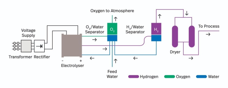
The flow of hydrogen, oxygen and water in a proton exchange membrane water electrolyser.
When a university installs its reactor in a commercial foundry, there are benefits for students, research groups and the chipmaker
BY RICHARD HOGG FROM THE UNIVERSITY OF GLASGOW
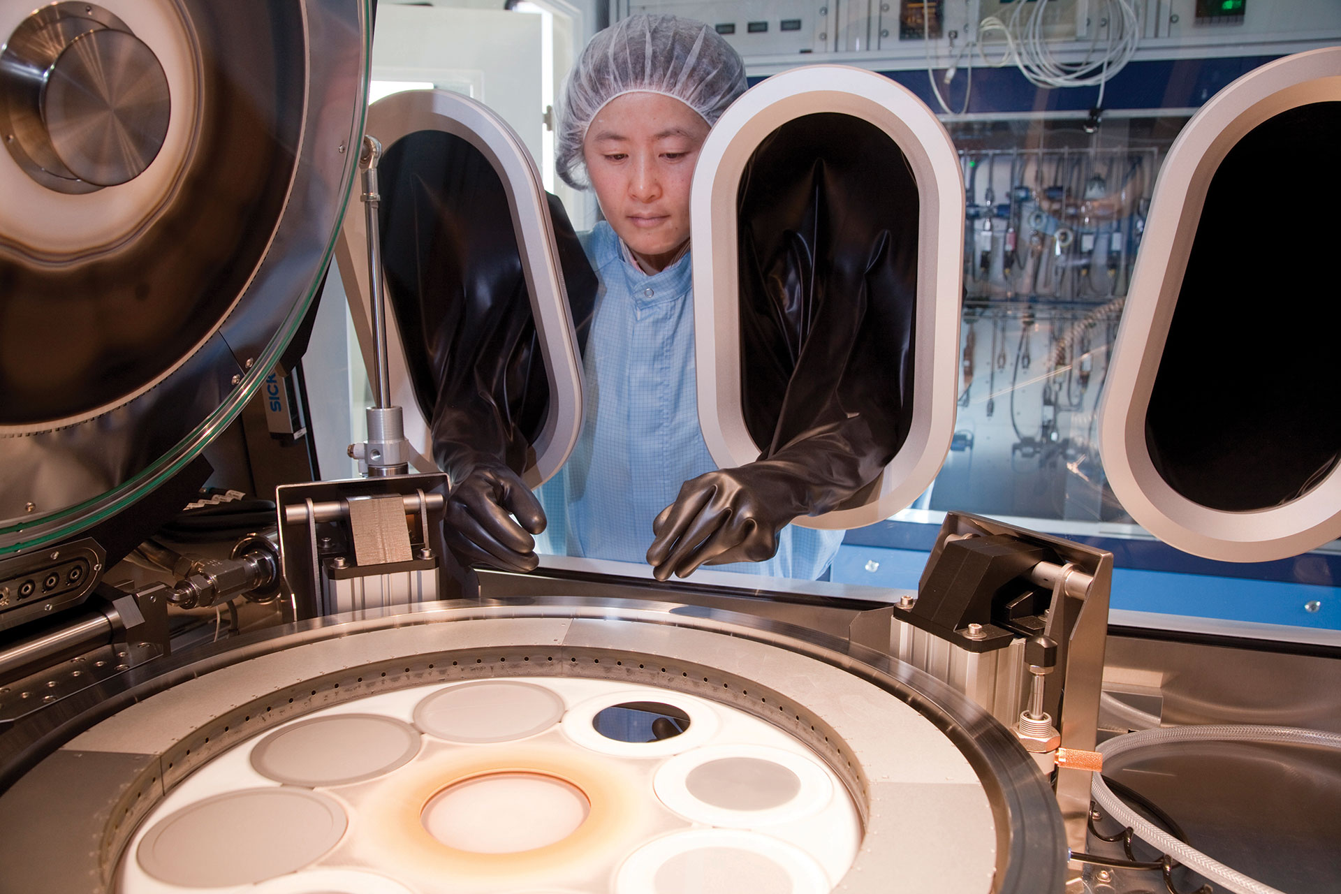
When business is booming, manufacturers of compound semiconductor devices find it a challenge to recruit PhD graduates with experience in MOCVD growth. Expertise on this front is highly valued because the growth of high-quality epilayers using this technique is a key process in the production of LEDs, lasers, solar cells and transistors.
However, it is unlikely that these PhD graduates will hit the ground running when they start work in a III-V foundry. Their skills have been honed on small tools designed for growing material for research purposes, in labs run in a manner that are research focused, and so not aligned with best practice for high-volume production. These new recruits will only be at their most productive after being given a chance to acquire the skills to run a high-throughput MOCVD reactor, housed in a cleanroom with a strict set of operating guidelines in terms of quality, yield, and cost.
But it doesn’t have to take this long to get up to speed.
The solution is to adopt another way of working: site the university’s MOCVD tool in an independent, volume-producer of III-V compound semiconductors. That’s the approach we are pioneering at the University of Glasgow, with our reactor housed at CST Global’s manufacturing facility in Blantyre, on the outskirts of Glasgow.
This new facility is jointly managed by ourselves and CST. This approach to operating an MOCVD tool is not just of great benefit to the PhD students. It’s also a winner for the research group, the chipmaker and the local economy.
Our students benefit from working in a commercial setting, with an MOCVD tool operating in a cleanroom complying with ISO 9001:2015 quality, the highest environmental and safety standards, housed besides foundry services. In this environment, our PhD students are rubbing shoulders with experienced engineers on a day-to-day basis. They therefore pick up informed, industrial knowledge, benefiting their development and employability. This unique environment targets the production of work with both commercial value and academic excellence. In turn, this allows us to to recruit high-calibre PhD students, being attractive to those who prefer to work in a commercial environment whilst studying, as it can make them more employable than those who dedicate their time to more fundamental work.
Another great advantage of our new approach is that the novel semiconductor materials and devices developed during our electronics and photonics research projects can be taken seamlessly from the laboratory to commercial, volume production. That’s obviously not the case when similar developments occur in universities with more traditional ways of working. In those environments, efforts to commercialise technology often require a senior academic to launch a start-up. That takes a lot of time and effort – but they are not the only drawbacks.
A far bigger issue is the clear conflict of interest between the commercial and academic worlds. In a commercial setting, a company must ‘feed’ a reactor with R&D and manufacturing work to ensure profitability and achieve a return on investment. Success requires an overhead of strong sales, administration, production and marketing infrastructures, not to mention a customer base to sell to. And the more repetitive the work the better, as margins rise when a tool is optimised for volume production of familiar, repeatable products. This is the domain of efficient business.
By contrast, a university, which holds charitable status, cannot operate effectively in a commercial environment. A university may undertake research projects for commercial entities, but these can be less inclined to further knowledge and understanding; instead they major on the development of manufacturing processes and rapid pay-back. A commercial focus therefore often conflicts with the academic aims of the university, where the measure of excellence is research with a high global impact. It is this metric that drives the ratings of our schools; the recruitment of our students; and the level of funding from research organisations and investment from the university. The majority of academics are driven by creativity, and judge their success by various factors, such as the number of citations of their high-quality research papers. Business accolades and efficient production often mean little to them, making their very involvement in managing a spin-off business a possible distraction.
Further benefits of housing a university-owned MOCVD reactor in a commercial setting relate to health and safety and the cost of ownership. Running an MOCVD reactor requires the use of potentially toxic, explosive chemicals. They can be costly to source, have long lead times, and are a security issue. And their use requires infrastructure to ensure safe handling of gases and their abatement. When the MOCVD reactor is sited in a commercial setting, these issues are far easier to address. That’s partly because it is far more likely that there are staff with experience of handling environmental protection procedures and legislation. What’s more, a university campus is, more often than not, a poor choice to house such a reactor. In our case, The University of Glasgow is surrounded by suburban regions of Glasgow and traversed by several thousand people a day. Additionally, many of our buildings are accessed very easily by our students and visitors. An industrial setting is clearly a far better option!
What about the benefits for the company that has a university-owned MOCVD reactor within its facility? Well, in the case of CST, by collaborating with us on cutting-edge research projects, it can identify the very best PhD talent available for recruitment. Three highly employable PhD students are currently coming through this route.
In addition, CST Global uses the MOCVD reactor for its research projects, including university collaborations, and has an agreed percentage of the reactor’s capacity reserved for its own work. This allows their other growth tools to concentrate on volume production. The CST custom foundry setting, where many separate confidential projects are executed on a daily basis has been beneficial in teaching me new working methods. These allow the MOCVD tool to be included in both highly collaborative working with CST, but also the development of devices and processes with trade secrets being developed and maintained with other collaborators.
Benefits of this way of working even extend beyond those for PhD students, universities and chipmakers: it is good for the nation. In Scotland, by leveraging our academic and commercial infrastructures, we are creating jobs and contributing to the UK economy. This should help us to attract more great people to come to Scotland, furthering our already strong photonics and electronics industries.

Professor Hogg heads a group that is researching device physics and engineering, epitaxial processes and fabrication technologies. These efforts are helping to develop diverse applications for semiconductor devices.
Hogg studied physics at The University of Nottingham, before completing a PhD at The University of Sheffield in Semiconductors. He has over 22 years of post-doctoral experience in industrial and university research, including at NTT Basic Research Laboratories (Japan) and in Professor Arakawa’s Laboratory at the University of Tokyo as an EU-Japan Fellow. He held a research position at Toshiba, Cambridge, and had a key foundry management role at Agilent Technologies, Ipswich, which was, at the time, the highest volume III-V facility in Europe. He has been Professor at the University of Sheffield, where he worked from 2003 to 2015 and is now Professor of Photonics and Head of Electronics and Nanoscale Engineering at the University of Glasgow.
Engineers at ISFOC have racked up more than ten years of experience in operating, optimising and analysing CPV plants. To find out what they have learnt over that time Richard Stevenson quizzes CPV technology manager Maria Martinez and maintenance manager Eduardo Gil.
Q Broadly speaking, how is ISFOC assessing the performance of CPV?
A Maria Martinez (MM). ISFOC is a public R&D company, and our focus is to foster and promote CPV industrialization. With this purpose, when we were founded in 2006, our goal was to carry out electric power-plant
installations with the CPV technologies available in those days. Up to 3 MW was the first idea.
Technologies were selected in a public call for tenders. In the first phase, three different suppliers were installed [at our headquarters] in Puertollano (Ciudad Real) and in a second location 300km away, Almoguera (Guadalajara).
We have 800 kW in Puertollano and 300 kW in Almoguera in operation and connected to the grid since September 2008. Puertollano is our main installation where most of the performance studies are carried out.
For the power plant of Puertollano, one supplier was Concentrix Solar, who became Soitec Solar in 2009, and since October 2016 is owned by Stace Electric. The second is SolFocus and the third Isofotón – for those two, the suppliers are not available, but we don’t know if in the future someone will begin working again with their products.
We have 200 kW of Concentrix – 36 concentrators of 5.5 kW. Each concentrator has its own inverter.
We have 200 kW of SolFocus. Here we have different types of concentrators, different versions, in order to test them. We have two concentrators of 7 kW; another 28 of 6 kW; and additionally, two more of 9 kW of a next-generation product, which were installed in May 2012. Each concentrator has its own inverter.
And then we have Isofotón. Here we have CPV plants and one flat-PV plant mounted on two-axis trackers, with the goal of making some comparison between CPV and flat PV performance. For the CPV plants we have 27 concentrators of 11.1 kW, with three centralized 100 kW inverters.
The first objective of all these installations was to help the suppliers. They had feedback about the qualification of the modules, the characterisation of the CPV plant, and the long-term performance. We were always collaborating with them and giving them our support to improve their products. All made new versions of their products that can be found here, in Puertollano.
We have a lab for the qualification of modules (standard IEC-62108) and trackers (standard IEC-62687). New developers have been always working with us. We can carry out tests to improve the product during the design phase.
We also have in our installations the prototypes of new developers, for instance Isofoton and Semprius. Isofotón installed in 2012 two concentrators of their last generation. Also, we have a prototype, but not connected to the grid, from Semprius. The CPV module of Semprius set a world record efficiency of 33.9 percent in 2012 and at ISFOC the real performance of the module in real operation in the field was assessed.
Q Is your local climate typical for a CPV installation?
A MM. No. We have a good, sunny summer, but during winter we have lots of cloudy days.
During the summer, when we have plenty of hours with high values of direct irradiance, we often observe peak values higher than 1000 watts per square metre. So, for assessing CPV, I think we are a good location, because we have high temperatures and high irradiance values. We also have some sunny and cold days that are very helpful to model CPV technology in best operating conditions – high irradiance and low temperatures.
The DNI in Puertollano is around 2,200 kilowatt-hours per square metre. It’s one of the highest values in Europe, but it is far away from values in South Africa or Australia, where they see 3500 kilowatt-hours per square metre.
Q The role of the compound semiconductor industry is to provide multi-junction cells that operate at high levels of concentration. So far, is it fair to say that your data suggests that the cells are up to this task?
A MM. Yes, although we are not experts in evaluating solar cells in depth, we can indicate that not too many issues, related to solar cells, have been detected so far.
We are members of the IEC committee, and what we see is that there is a lot of effort being carried out to improve the efficiency and performance of CPV cells, keeping always in mind the reliability of the devices.
CPV optics focusing the sunlight onto a CPV cell
A: MM. The first thing that I want to remark is that this module was used for making the installation here in 2007. At the beginning of the project, all the technologies were required to pass some IEC-62108 tests to ensure the reliability of their design, and this technology was failing some of the tests.
In Spain, in those days, a feed-in tariff existed for PV installations, and to obtain those benefits it was mandatory to connect our plants before September 2008, since an important income for ISFOC comes from selling this electricity. Therefore, we decided to go ahead with the installation of this version of the product, although we knew it was failing in some lab testing.
On the one hand, from an R&D point of view, this was a great opportunity to verify if the failures detected in the lab were going to be reproduced in the field. On the other hand, we had a contract with the manufacturer, to maintain our income. If the failures were reproduced, affecting the performance, they would replace some of the concentrators. Finally, failures were repeated in the field. In 2012, they replaced the 18 kW with a new- generation product that was IEC-62108 certified.
The first issue occurred in the first years. It was the gasification of some of the materials inside the module, that were deposited over the optics surface. The effect is like some scattering of the light, reducing the energy that reaches the cells.
There was also some damage to the secondary optics caused by the concentrated sunlight, some kind of failure in the reflective coating.
The most important result that we obtained from this experience is that the IEC-62108 standard is working. It was possible to detect in the lab, with tests, some of the failures occurring in the field.
But some other failures were not possible to detect, so further work is needed in the standardization committee to modify the tests if possible. Failures related to long-term exposure to direct or concentrated sunlight are
not so easy to reproduce.
Q: Do you think that when designed with skill and care, modules can be robust, showing minimal degradation?
A: MM. Yes. We have some technologies that have been operating for more than ten years. Up to now, everything is working at the same level as it was in the beginning.
It’s also important to say that our installations are prototypes. The next products were even better than the ones we have here.
Q: Based on your data, what have we learnt about the reliability of tracker designs?
A: Eduardo Gil (EG). I would like to remark that our trackers are based on preliminary designs. At the time, the CPV community focused its efforts on developing CPV modules to be as efficient and reliable as possible. When we started operating and maintaining our CPV power plants, we started to be aware of the importance of other components.
We learnt that the identification of all key components responsible for the vast majority of unavailability is essential to reduce unplanned intervention, increasing the reliability of the trackers. However, if reliability and maintainability weren’t taken into account during the early stages of the design, when the cost of making any change is cheaper, the cost of increasing the reliability during the operation time would be unaffordable.
Q: Do you see any concerns relating to reliability when moving to higher concentrations, such as focusing light by 2000 suns rather than 500 suns?
A: MM. We are not experts in cells. Going to a higher concentration means that more heat dissipation in the module and the cell is needed. Most modules have passive cooling. And perhaps higher concentration will require active
cooling, which it is not desirable because it would be more complex and expensive during installation and O&M tasks.
We have systems here with small cells that are working up to 1000 suns. But going to higher concentration, in my view, may require a move to dense CPV receivers with solar dishes or parabolic mirrors, including active cooling for heat dissipation – like Solar Systems, Raygen, in Australia.
I know that one way to reduce the cost of a concentrator is to increase concentration without increasing the cost of the rest of the elements. But I think that perhaps 2,000 suns is too high at present.
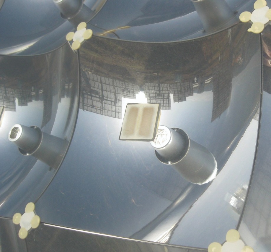
A CPV receiver illuminated through a multi-phase reflective optic
Q: To me, it is the parts of the system that I have given little thought to that are to blame for the most failures. These are control systems and firmware. Why have they been so problematic? And can these weaknesses be addressed?
A: EG. Not all software and firmware is problematic. That only occurred with one of our partners who decided to design their own inverter, due to the fact that there wasn’t in the market any specific inverter for CPV technology.
We also suffered from hardware issues. That inverter included the control system in the same box. It had caused several problems, because of the heat generated inside.
Thanks to our data analysis and support, they improved the software and were aware of the heat dissipation problems.
Some years later, some inverter manufacturers adapted their design for CPV technology. This partner decided to use commercial inverters in their system, avoiding the problems of the combination of inverter and the controller of
the tracking system.
Q: A significant proportion of CPV downtime is also due to issues associated with encoders and limit switches. What’s the role of these components, and can they be improved?
A: EG. A tracker usually has two encoders: one for the elevation axis, and one for the horizontal axis. Basically, the encoder is a counter. It sends the position of the tracker to the control board.
Regarding the limit switch, it is used to prevent the tracker from reaching a forbidden position during operation. It’s a normally closed contact, but when it is pressed, the contact opens and stops the current.
We now have more than ten years of experience in the operation and maintenance of tracking systems. We have detected many of these components located in an improper place. Most of the time, the encoder is in a place where, for example, water can get inside; if it were better located, it would work properly. It’s not really a problem with the component; it’s a problem with the design of the tracker.
Q: Now that the most likely causes of failure for a CPV system have been identified, what figures should be possible for uptime and annual degradation?
A: EG. Up to now, we don’t have enough records to answer this question. In our opinion, the degradation of mechanical parts is always a controversial topic and depends on not only the maintenance strategy deployed but also on the operational environment where the CPV is installed. High winds, extreme temperatures, heavy rains, etc., will play an important role.
MM. And if we talk about degradation of the CPV technology itself, the CPV modules, we can say that this is one of our fundamental analyses. We are continuously analysing the performance of the CPV plants but filtering out all the data related to maintenance and operation incidences, which means analysing the performance of the CPV technology only. We compare the energy of production with the DNI accumulated for the different years of operation. What we have up until now – and what we hope will continue in the future – is that the level of degradation is less than one percent per year. It’s in the same level as flat PV.
Q: Is there a role for preventive maintenance in the operation of a CPV plant?
A: EG. Of course there is a role for preventive maintenance in the operation of CPV plants. Preventive maintenance is essential for boosting the market confidence of this technology. Many people believe that maintenance is an extra cost, however, from our point of view, it’s an investment. During the first years of operation of our CPV power plants, we evaluated and adapted all the operation and maintenance protocols for CPV technology, which allowed us not only to increase reliability of our CPV power plants, but also to reduce drastically the maintenance costs, increasing the uptime of the systems installed at our facilities.
The main idea is that we pay for maintenance to gain reliability and availability of our CPV plant. Optimised maintenance strategies increase production revenue, and that means more income for the investor.
Q: You have found that operation incidences would be lower if more support were given by suppliers. But some suppliers are no longer in business. That must be a concern for efforts to rejuvenate this industry, as investors in CPV will want to be supported by system makers that will be in this industry for many years to come?
A: MM. Economic issues have really strangled the photovoltaic sector.
Manufacturers of CPV were trying to develop a different product, like some special PV technology, so for them it was even more difficult to obtain funds from banks or investors. Without investment, you cannot make any improvement to the technology. A lot of companies were pushed to close their business, because of this crisis.
I think, and hope, that new CPV developers will not suffer from this issue. The story of Concentrix, Soitec and Stace Electric shows that if you have a good a product, someone will have confidence in it.
I hope that in the near future we will have again big partners in this industry.
Q: Compared to the figures quoted about a decade ago, is the levelised-cost-of-energy coming down, due to a greater understanding of reliability issues?
A: EG. The levelised-cost-of-energy is coming down due to two main reasons. On the one hand, the CPV installation cost has dropped significantly from 2009 to 2018 – this fact strongly affects the levelised-cost-of-energy.
On the other hand, our maintenance strategy has allowed us to increase reliability. In other words, it has allowed us to reduce the maintenance cost, so the levelised-cost-of-energy also comes down because of this cost reduction.
Moreover, it is important to remark that year-after-year, the three-junction cells are beating the efficiency record. This also helps to reduce the levelised-cost-of-energy.
Q: Do you see any signs for a possible re-birth of the CPV industry?
A: MM. Yes, I think so. Inside the community, what we see is that again there are new developers, university researchers and small companies fighting to demonstrate that their product has a place in the electricity generation market.
A sample of active companies nowadays: BSQ Solar, Spain; Raygen, solar dishes and central tower receivers, Australia; Morgan Solar, Canada; MagPower, Portugal; and don’t forget about Stace Electric, Canada, who currently owns the technology of Concentrix Solar.
Moreover, we must name some projects that are funded by public entities, such as CPV4all and CPV Match, demonstrating that there are some interesting developments in CPV.
Finally, it must be said that there are new CPV concepts under development that could enlarge the market of the technology – like hybrid CPV-thermal systems, which use an active cooling of the solar cells to warm up fluids – or BICPV – building integration CPV – that are being explored by the CPV community.

One of the CPV plants located at ISFOC headquarters
Satellites could be powered by incredibly efficient modules featuring five-junction micro-cells and tiny glass lenses
BY MATTHEW LUMB FROM GEORGE WASHINGTON UNIVERSITY
By far the most efficient class of technology for converting sunlight into electrical power is the high concentration photovoltaic (HCPV). Modules that are based on this technology use low cost lenses or mirrors to focus sunlight onto multi-junction cells with three or four junctions, to realise conversion efficiencies at the cell level that are nearing 50 percent. Note that the focusing of sunlight by factors of typically 500 to 1,000 is critical to increasing the bang-per-buck of this technology: it spawns a hike in conversion efficiency, as well as slashing cell costs, due to a dramatic reduction in the amount of compound semiconductor material required to deliver a given output.
The commercial success of HCPV has been thwarted by several factors, limiting this field to a handful of companies. Arguably the most damaging of thorns has been the rampant success of low-cost, large-area solar cell technologies, particularly crystalline silicon. But there are other issues, such as the requirement for precise two-axis tracking, which adds cost and complexity to an installation, while limiting packing density due to shadowing. Another impediment is that it is impossible to focus diffuse light with conventional optics, so utility-scale CPV is restricted to desert-like locations, where the diffuse sunlight fraction is small.
One glimmer of hope is that conventional, large-area silicon solar panels are now beginning to push firmly against their fundamental efficiency limits. So, if a large boost in HCPV efficiency came along at low cost, and were combined with the remarkably high energy yield available from two-axis tracking of the sun, this solar technology could be highly competitive once again.
Further cause for optimism is the emergence of myriad niche applications where the key requirement is maximising the number of watts per square meter, rather than the cost per watt. The former metric is the priority in remote and space-confined applications, such as bicycle and car-charging stations; in temporary DC microgrids, such as those used for disaster response; and in the application we will focus on in this article – space power.
Cell considerations
During the last decade, many CPV companies have closed up shop. But the majority of cell suppliers have not suffered the same fate, thanks to a healthy market for III-V multi-junction solar cells in space. Here they are the established industry leader, with numerous multi-junction solar cells on the market. Success stems from a different set of priorities: cost-per-watt is a secondary consideration, and topping the list is the specific power, judged in watts-per-kilogram, and the volumetric power density, evaluated in terms of watts-per-cubic-metre.
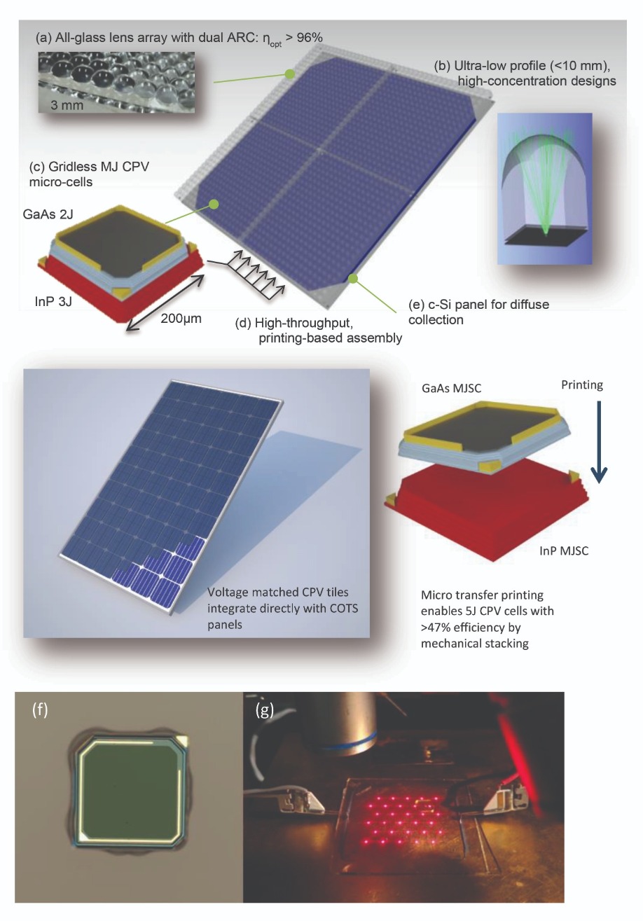
Figure 1. (a)-(e) The main features of the micro CPV design, which has been developed by a team that is led by researchers at George Washington University. Modules incorporating state of the art CPV microcells, all-glass optics and diffuse collection using off-the-shelf crystalline silicon solar panels. (f) A GaAs-based dual-junction microcell transfer printed on to a glass substrate. (g) A hexagonal array of dual-junction microcells under forward bias, operating as LEDs.
The need for a high specific power reflects the very high launch cost for putting anything in space. Regardless of what it is, it costs in the region of $10,000 per kilogram. So, to drive down launch costs, solar cell suppliers try to produce the lightest weight cells possible.
The other key consideration is the volume of the payload. To minimise this, extremely creative and hi-tech photovoltaic panel deployment systems are employed on satellites. They feature low profile modules and large-area, III-V multi-junction solar cells with industry leading performance.
Devices that work well on earth may not do so in space, due to the far higher levels of radiation that degrade material quality and reduce efficiency. To minimise this over the lifetime of the cell, suppliers encapsulate their devices in tens to hundreds of microns of cover glass. This coating shields the semiconductor layers from radiation, but adds significant weight to the final product.
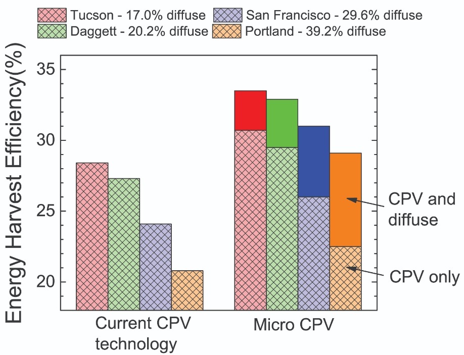
Figure 2. Predicted DC global energy harvest efficiency (annual kWh production / annual global resource on a two-axis tracker) in locations with different diffuse contents for conventional HCPV and a micro-CPV array.
CPV in space?
There have been several notable, successful experiments based on taking CPV panels into space. These efforts, aimed at exploiting the high efficiency of the technology to increase specific power, have focused on low concentration demonstrations that have failed to gain a strong foothold. But this time it could be different, thanks to the advent of a new type of CPV technology – micro CPV. Its timing could not be much better, given that multi-junction cells operating at one sun are reaching practical limits for efficiency and specific power; and the advent of reusable rockets, coupled with large increases in space traffic, could drive down launch costs.
Helping to develop a new generation of CPV technology for space is the US Department of Energy’s Advanced Research Projects Agency-Energy (ARPA-E). Through the programme MOSAIC – Micro-scale Optimized Solar-cell Arrays with Integrated Concentration – it is funding 11 teams with a total of $24 million.
The efforts that ARPA-E are supporting include those by our team at George Washington University, working in partnership with researchers at the US Naval Research Laboratory, Veeco, Northwestern University, MIT and X-Celeprint. Together, our collaboration is aiming to address some of the main obstacles facing conventional HCPV by marrying ground-breaking, ultra-high-performance five-junction cells with all-glass lens arrays and a glass backplane (see Figure 1 for an overview). Our glass lenses feature a novel, bifacial anti-reflection coating that provides an extremely high optical efficiency while concentrating sunlight by a factor of approximately 500.
One of the great strengths of our modules is that they can capture diffuse light, thanks to the incorporation of a bifacial, crystalline silicon solar panel. Attaching this to the CPV module injects a significant boost to the overall power output, especially in locations where a large fraction of the total solar resource arrives as diffuse illumination (see Figure 2).
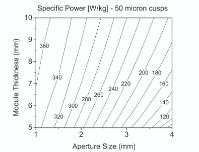
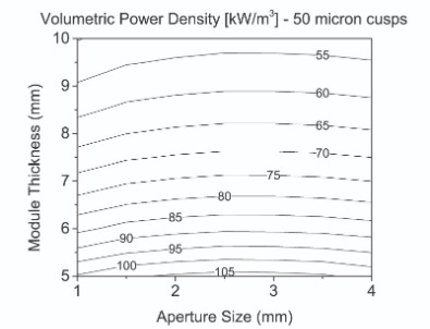
Figure 3. Specific power and volumetric power density for different lens designs for the five-junction CPV cell developed by the team led by researchers at George Washington University.
Our micro CPV module is also able to excel in efficiency. The apertures for our CPV cells are just 170 μm by 170 μm, so the devices are small enough to avoid the use of metal grid fingers when efficiently extracting current from the cell. Instead, a single metal contact is employed at the edge of the aperture, eliminating shadowing loss. Another benefit of using microscale cells is that they simplify thermal management. Thanks to this, cells can operate at lower temperatures, thereby churning out power at higher efficiencies.
We assemble our microcells with a micro-transfer printing process, a technology commercialized for PV by former CPV company and team partner Semprius. Note that this is also the core technology of our industry partner, X-Celeprint: it applies micro-transfer printing to a range of micro-optoelectronic applications.
Micro-transfer printing allows precise, parallel assembly of microscale devices that are removed from their native substrate with a wet etch procedure. In addition, we use micro transfer printing to heterogeneously integrate dual-junction, GaAs-based solar cells with triple-junction InP-based solar cells. The five-junction cells that result – featuring high quality, lattice-matched materials – capture a broad range of the solar spectrum. Do this at low cost, and it can be disruptive to conventional PV technology.
Our CPV module is well-suited for use in space. Its merits include: a very high radiation tolerance, thanks to shielding by the glass lens array; a reduced arcing risk between cells, due to their large separation; and a low profile module, enabled by focal lengths of just a few millimetres. Those dimensions allow units to be drop-in replacements for conventional panels, and be compatible with existing deployment techniques.
In missions to deep space, it’s actually an advantage to operate multi-junction cells at high concentration. That’s because this negates many of the difficulties associated with low-temperature, low-intensity environments. These issues, which include complications arising from hetero-barriers and trap states, are encountered on missions to parts of the solar system much farther from the sun.
Yet another strength of our CPV modules is that they have the potential to be far cheaper than large-area III-V solar cells. This benefit will become increasingly important in the future, due to decreasing launch costs.
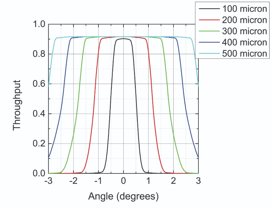
Figure 4. Optical throughput versus incident angle for glass lenses with a
Sweet spots
Modelling suggest that the efficiency of our CPV cell in space peaks at roughly 200 suns. Go any higher and performances falls due to temperature-related losses and series resistance. Note that lower values of concentration are used in space than on earth, due to the lack of convective cooling, which impairs thermal management. A higher cell efficiency does help thermal management though, as less wasted power is required to be dissipated.
We have evaluated the specific power and volumetric power density of our module for different lens aperture sizes, while assuming all-glass lens arrays with square apertures (see Figure 3). In this study, our 1 mm by 1 mm lens aperture provides a concentration of about 35 suns, while the 4 mm by 4 mm aperture offers a concentration of 550.
The smaller lenses are compromised by a lower optical efficiency, due to a ‘cusp’ region that extends for about 50 μm along the perimeter of each lenslet. This flaw, resulting from the surface tension of glass as it cools in the mould, hampers the focusing of light from the cusp region. However, even with this imperfection and the lower concentration, the smaller lens yields a higher specific power. That’s because these lenses are lighter, thanks to the combination of their smaller apertures, and their lower lens curvature, due to a longer focal length.
Unfortunately, from the perspective of maximising the volumetric power density, it is better to use a lens with a shorter focal length. The highest density values coincide with concentrations that correspond to the peak cell efficiency.
This creates a conundrum that is not faced by the designers of conventional flat panel designs, which produce highest specific power when delivering their highest volumetric power density. However, there is a happy medium for micro-CPV modules in space: small aperture lenses with a short focal length. In future, it may be possible to make even lighter lens arrays using Fresnel lens concepts – this would improve the specific power even more.
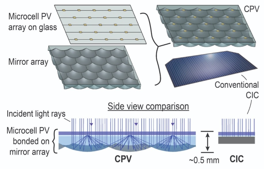
Figure 5. A reflective microcell CPV array is hardly any thicker than a conventional coverglass-integrated space PV cell (CIC).
Wherever CPV systems are used, arrays must be pointed directly at the sun to maximise power. This is not as daunting to realise in space as it might first appear, as most satellites can track the sun to within a degree or so, using a variety of attitude control systems. However, the danger is that if the design employs a narrow acceptance angle, a significant pointing inaccuracy runs the risk of a power outage.
The good news is that it is easy to avoid this scenario, because the economics of space are in our favour. To highlight the way forward, we have considered the optical throughput efficiency for broadband illumination at varying incident angles, for a 1 mm square lens, 5 mm module thickness and a variety of CPV cell sizes (see Figure 4). This study shows that by oversizing the cell, a much wider angular acceptance is possible. There are penalties to pay, in the form of a slightly reduced cell performance – solar cells generally work best when uniformly illuminated – and, of course, a higher overall cost, due to an increase in semiconductor content. However, even with those oversized cells, the cost of the panel is still an order of magnitude lower than an equivalent one with no concentration.
The work described so far considers refractive optics for a space concentrator system. But that is not the only promising option: there is also much potential with a reflective concentrator geometry (see Figure 5). Those of us at George Washington University are pursuing this as well, in a partnership with a team at Penn State University, led by Chris Giebink. Modules are formed by printing microcells on a thin sheet of glass, which is subsequently bonded to a reflective lenslet array.
One of the primary merits of CPV modules with reflective optics is that they enable cells to operate near the thermodynamic limit of concentration, while the optics have a far lower aspect ratio – the thickness, divided by the aperture width, may be as low as 0.25. With such a design, mass can reach a new low, while increasing the angular acceptance for a given concentration ratio.
For example, for 170 μm by 170 μm cells operating
at a concentration of roughly 35 suns, the total thickness of a practical concentrator can be as low as 0.5 mm – that is comparable to the thickness of existing coverglass-integrated space PV cells – while the angular acceptance can be as high as approximately ±5˚.
A practical challenge with this type of module is the extraction of heat from the cells, because they are embedded in low thermal conductivity glass.
This should be manageable, according to thermal modelling and experimental measurements on a similar, terrestrial microcell CPV. However, we can only be certain of this after we have experimentally tested this design.
We have no doubt that micro CPV offers exciting new opportunities for lightweight, low-cost, low-profile CPV arrays that set a new benchmark for efficiency. Armed with funding from ARPA-E, the new, state of the art CPV modules that we are developing using micro transfer printing promise to have benefits on earth and up in space.
The performance of the UV LED improves by trimming its dislocation density, boosting light extraction and enhancing thermal management
BY NEYSHA LOBO PLOCH FROM UV PHOTONICS AND FBH, AND MICHAEL KNEISSL FROM TU BERLIN AND FBH
Sales of the UV LED are rising, as more devices are being deployed in applications ranging from the disinfection of water, air and surfaces to medical diagnostics, phototherapy, and the curing of various materials. The success of this device is driven by its superior attributes to the incumbent source, the mercury lamp. The UV LED can be turned on and off in an instant, it doesn’t run hot, it is environmentally friendly, radiation hard, and its emission spectra can be selected to cover almost anywhere in the UVA, UVB and UVC range. What’s more, it has a low operating voltage, a compact size and it is robust, making it ideal for portable, battery powered applications.
Despite all these strengths, sales revenue for the UV LED is still dwarfed by that for the mercury lamp. That’s partly because fabrication technologies for this class of device are still at an early stage, and large-scale manufacturing is yet to take place.
There are also other issues, related to performance. Conversion efficiency for the UV LED is far lower
than that for its blue cousins, and is below ten percent in the UVB and UVC. And lifetime is far shorter: UVC LEDs may last for only a few thousand hours, or even a few hundred. These weaknesses crank up costs associated with ownership and maintenance, and are a barrier to a commercially successful, widely deployed technology.
To improve the commercial viability of the UV LED, there needs to be improvement in the lifetime,
wall-plug efficiency and external quantum efficiency. The good news is that for the most part, values for these characteristics are not held back by fundamental physical limitations, but can be increased by refining the fabrication technology.
Developing efficient devices
At UVphotonics, working in partnership with the Joint Lab GaN Optoelectronics that has been established between Technische Universität Berlin (TU Berlin) and Ferdinand-Braun-Institut (FBH), we are trying to address these key weaknesses of the UV LED. Our efforts are focused on increasing the efficiency and reliability of devices that are grown by MOCVD and emit in the UVB and UVC. The devices that we have made span 340 nm to 218 nm (see Figure 1).
To drive the development of devices that are cheaper, more powerful and longer lasting, we are evaluating and optimising each step of the LED fabrication chain, from growth of the different semiconductor layers with varying material compositions that make up the LED heterostructure to the packaging of the individual chips.
The first decision facing any maker of UV LEDs is the choice of substrate. We have chosen sapphire: it is optically transparent, low in cost and available in diameters up to 8 inches.
Sapphire’s weakness is that it has a large lattice mismatch with the AlGaN layers of the UV LED. This results in threading dislocations, generated at the interface during growth. If these defects propagate to the active region, where light is generated, they act as non-radiative recombination centres, pegging back device efficiency. According to simulations and experiments, this influence is so severe that the output power of 280 nm LEDs can more than halve when the threading dislocation density increases from
1 x 109 cm-2 to 5 x 109 cm-2.
To reduce the detrimental effects of threading dislocations in our UVB LEDs, we use thick AlN layers, followed by a strain management section, made of alternating thin layers of GaN and AlN. With this approach, the threading dislocation density is about 3 x 109 cm-2.
At even shorter wavelengths, dislocations are even more detrimental to efficiency. To combat this, fabrication of our UVC LEDs begins with epitaxial lateral overgrowth, to reduce the threading dislocation density down to around 1 x 109 cm-2.
We are currently investigating other promising, cost-effective techniques to reduce the threading dislocation density. They include sputtering AlN on sapphire, followed by annealing at high temperatures, to obtain a high-quality crystalline layer.
The growth of our UV LED structure begins with the silicon-doped n-type AlGaN layer, which must combine transparency at the emission wavelength with high electrical conductivity for homogeneous lateral current-spreading. After this is the active region, containing several AlGaN or InAlGaN quantum wells, followed by an electron-blocking layer that prevents electrons from escaping out of the active region, and a highly conductive magnesium-doped p-type AlGaN layer for hole injection.
Figure 1. Normalized emission spectra of III-nitride based UV LEDs fabricated within the Joint Lab GaN Optoelectronics between TU Berlin and FBH Berlin. © TU Berlin
These LED epiwafers are processed into lateral geometry devices using standard lithography techniques. A laser scribing and dicing process follows, to create individual die. Using this approach, we have produced 310 nm UVB LEDs with a 30 mW output at 350 mA. After burn-in, the extrapolated lifetime – evaluated in terms of the time taken for the output power to halve – is 8,000 hours.
As expected, moving to shorter wavelengths reduces the output: at 265 nm, which is in the UVC, our devices deliver a 25 mW output at 350 mA. At the even shorter wavelength of 233 nm the output is just 0.3 mW at 100 mA. Note that this result is obtained for one of the first fully packaged UVC LEDs worldwide to produce a single emission peak at such a short wavelength.
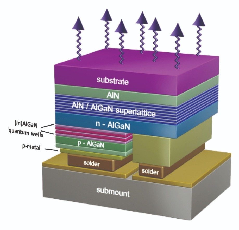
Figure 2. A flip-chip mounted III-nitride based UV LED die. © TU Berlin
In every LED, not all of the light that is generated within the active region exits the chip. But this situation is more severe in UV LEDs, as the high refractive index of the AlGaN layers increases the total internal reflection, leading to a hike in the absorption of UV light within the device. In particular, light is lost at the metal contacts and the p-AlGaN hole-injection layers.
Another issue with UV LEDs is that light extraction is influenced by changes in the valence band structure of the group III-nitrides. As the emission wavelength decreases – due to increases in the aluminium content in the quantum wells – the polarization of the emitted light changes. At longer wavelengths, emission is mainly transverse electric polarized with respect to the surface normal of the (0001) c-plane oriented sapphire substrate, but as emission heads deeper into the UV, polarization becomes predominantly transverse magnetic. This orientation leads to a lower light extraction from the chip.
According to extensive experimental and theoretical studies, the switch from transverse electric to transverse magnetic takes place at around 240 nm. However, this crossover point can be shifted by changes to the substrate orientation, and to the strain and confinement within the quantum wells.
For a typical UVB LED that is not equipped with any light extraction features, simulations suggest that just 8 percent of the light that is generated in the active region exits the chip. And at shorter wavelengths, this figure is even less. Consequently, light extracting technologies are essential for realising high-efficiency devices.
Our team is developing two approaches to boost light extraction: transparent p-current spreading layers, combined with a reflective low-resistant p-metal contact, such as a transparent ITO layer together with an aluminium reflector; and growth on patterned sapphire substrates. With the latter, light extraction efficiency rises via an increase in the direct extraction of light and a randomisation of the angular distribution of the photons in the LED.
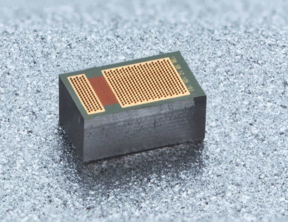
Figure 3. Single UVB LED chip with gold stud-bumps deposited by electroplating at the wafer level. © FBH /schurian.com
Downsides of low wall-plug efficiencies are not limited to a low output power. With less light getting out, more heat is generated within the chip. That’s a big issue, as higher temperatures impair the electrical and optical characteristics of the LED, and also speed its degradation.
The most common approach to prevent an UV LED chip from overheating is to flip-chip bond the low thermal conductivity sapphire die to a material that can suck the heat away. With this approach, the die is bonded epi-side down, enabling heat to transfer efficiently to the metal bonding pads (see Figure 2).
It would be a mistake to combine this flip-chip device with inexpensive, readily available alumina ceramic packages that are commonly used for visible LEDs and have a limited thermal conductivity. Far better is one of the newer packages being developed for deep UV LEDs that feature AlN ceramic layers with thermal conductivities of 150-170 W m-1 K-1.
These packages are far from ideal, though. As well as being pricey – they are more than a dollar a piece – it is difficult to integrate them with an aluminium UV reflector. In addition, device encapsulation is tricky, as the majority of state of the art, high-index transparent silicones and epoxy resins that are used in visible LEDs are not stable when exposed to high-energy UV photons.
Given these issues, today’s packaged deep-UV LEDs tend to include UV transparent quartz windows or lenses. This adds to the price, and can increase the complexity of manufacturing, because integrating quartz lenses into the device is challenging. Clearly, the development of inexpensive packaging materials for deep-UV LEDs is pivotal to commercial viability.
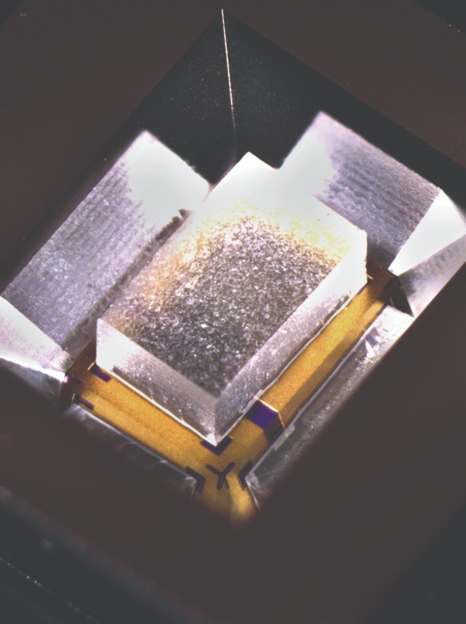
Figure 4. 320 nm LED flip-chip mounted in a silicon package. The package is developed by the CiS Research Institute forMicrosensors, Germany © CiS
In collaboration with our partners at the CiS Research Institute for Microsensors, we are developing a silicon-based package for UV LEDs (see Figure 4). Drawing on our collaborator’s great expertise in silicon technology, we are able to develop a cost-effective package that combines a low thermal resistance with the integration of versatile features, such as an aluminium reflector for increased light extraction, integrated diodes to prevent electrostatic damage, and monitoring sensors.
What’s next?
The UV market is definitely on the up, with ever more companies competing for sales. There is tremendous acceleration in the pace of development of UVB and UVC LEDs, and in the coming years, the focus will be on the development of advanced technologies to increase light extraction and on cost-effective packages exceling in thermal management.
Two of the biggest issues are arguably lifetime and the cost-per-watt. A far longer lifetime is needed to ensure stability of the UV LED systems for real world applications. Meanwhile, while today’s bang-per-buck of around $1 per milliwatt might be good enough for early adopters, breaking into the mass market will require a seismic shift to around $1 per watt for devices delivering far longer lifetimes.
The authors acknowledge the support of the Federal Ministry of Education and Research (BMBF) of Germany within the Twenty20 initiative Advanced UV for Life. The consortium Advanced UV for Life consists of 50 German industrial and academic partners working together on the development and application of UV LEDs. This effort is coordinated by the Ferdinand-Braun Institut, Leibniz Institut für Höchstfrequenztechnik, Berlin, Germany.
Further reading:
N. Susilo et al. Appl. Phys. Lett. 112 041110 (2018)
F. Mehnke et al. IEEE J Sel Top Quantum Electron. 23 1 (2017)
T. Kolbe et al. Materials 10 1396 (2017)
J. Rass et al. Proc. SPIE 9363 93631K (2015)
C. Reich et al. Appl. Phys. Lett. 107 142101 (2015)
J. Glaab et al. J. Appl. Phys. 123 104502 (2018)
M. Kneissl, J. Rass (Eds.), III-Nitride Ultraviolet Emitters-Technology and Applications, Springer Series in Materials Science, ISBN 978-3-319-24098-5 (2016)
Applications for UV sources
There are many applications that can be served by LEDs operating in the UVA (315 nm to 400 nm), UVB (280 nm to 315 nm) and UVC (100 nm to 280 nm) ranges.
LEDs emitting in the UVA and the UVB can be used for the industrial curing of resins and polymers, a process that hardens the surface and enables the production of abrasion-proof products. However, the primary applications for UVB LEDs are phototherapy for the treatment of skin diseases, such as psoriasis and vitiligo, and plant growth lighting for the targeted triggering of secondary plant metabolites.
For UVC LEDs, the largest market is the disinfection of water, air and surfaces. Here, the fast turn-on of emission and the ability to be electronically dimmable and compact in size, offer unique advantages for the design of energy-efficient systems that are customized for large-scale applications and small mobile systems. For very-short-wavelength UVC LEDs, there are also opportunities associated with non-line-of-sight communication, as well as basic science experiments in the area of gravitational sensors.
Additional opportunities for UVB and UVC LEDs are the detection of gases, such as SO2, nitrous oxides and ammonia, and analysis of DNA, RNA and other biomolecules.
Armed with minimal wafer bow, good wavelength uniformity and an internal quantum efficiency exceeding 80 percent, the 200 mm GaN-on-silicon epiwafer is an ideal ingredient for making displays
BY Liyang Zhang, Kai Liu, Peng Xiang, Hongjing Huo, Ni Yin and Kai Cheng FROM ENKRIS SEMICONDUCTORS
Flaws hamper the two incumbent display technologies, which are based on liquid crystals and organic LEDs. Those that feature liquid crystals are compromised by the complex architecture: each individual sub-pixel consists of a backlight, polarizers, a matrix of liquid crystal, and colour filters. This leads to a low efficiency. With OLEDs, efficiency is addressed, but at the expense of lifetime and reliability.
A far more promising option for making a display is an array of microLEDs. Each of its pixels is formed with an LED with dimensions of less than 30 mm that has the strengths of its bigger brother. Those merits include a high brightness and contrast ratio, a low power consumption, a fast response time, a long lifetime, a wide range of operating temperature and a wide viewing angle.
Armed with all these attributes, the power consumption of a microLED is very low. It’s just
10 percent of that of a liquid crystal display, and half of that of one based on OLEDs. The low power consumption does not hold back the brightness of the microLED display: it can be as bright as that made from OLEDs, while using just one-tenth of the OLED’s emitting area.
On top of all these strengths, gains may be realised from the smaller pixel size. This makes microLEDs an excellent candidate for transparent display applications – and it opens the door to integrating, in the spare space between the emitters, sensors and circuits. Adopting this approach enables the construction of displays with embedded sensing capabilities, such as fingerprint identification.
Thanks to the remarkable set of properties listed above, the microLED can be used in many applications, including large TVs, smart watches and wearables, virtual reality and automotive head-up displays. Consequently, the microLED display is regarded as a leader of next-generation display technology.
Figure 1. An LED epistructure used by Enkris for making devices on 200 mm silicon.
There are two options for fabricating microLEDs: monolithic integration and mass transfer. For applications like wearables that have less than 1000 pixels per inch, the ‘pick-and-place’ approach is used for massively parallel transfer. However, when microLEDs are used to make high-resolutiondisplays – that is those that have more than 1,000 pixels per inch – pick-and-place is not feasible. In this case, the monolithic integration of arrays is a better approach to producing high-resolution displays, because it can directly transfer a processed LED wafer to a target backplane through wafer-bonding technology.
For this latter approach, production ideally involves the use of large, flat epi-wafers with a narrow wavelength bin range and a low defect level. Flatness is important, because it allows the epiwafer to be transferred directly to a target backplane through wafer-bonding technology. A narrow spread of wavelengths is highly advantageous, because it can eliminate time-consuming die binning; and a low defect level is critical to improving final yield.
Requirements for the epiwafer may be specified as follows: a wafer diameter of at least 150 mm, to ensure high transfer efficiency; a wafer bow below 30 mm, to enable a high bonding yield; a wavelength uniformity that places die in a ±1 nm bin, so that display production is binning free; and a combination of a high internal quantum efficiency and a high light extraction efficiency, ensuring high brightness.
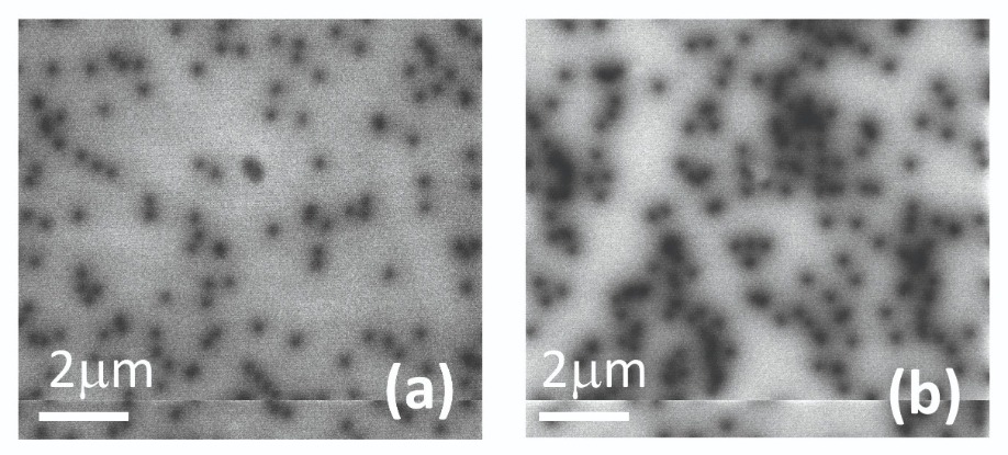
Figure 2. Cathodoluminescence reveals the threading dislocation density of unintentionally doped GaN on a (a) 200 mm silicon substrate and a (b) 100 mm planar sapphire substrate. Densities of threading dislocations are estimated to be 1.5 x 108 cm-2 and 1.9 x 108 cm-2 for (a) and (b), respectively.
At Enkris Semiconductor, China, we believe that the best way to fulfil all of these requirement is to produce LED epiwafers on silicon substrates. That’s because silicon is available in sizes of up to 300 mm in diameter, cost is low – it is less than $50 for a 200 mm substrate – and this material can provide the foundation for epiwafers with a high
quality and a low particle level. What’s more, GaN-on-silicon offers the advantages of compatibility with mature silicon-based manufacturing, which has well-established technologies for thin-film processes and the monolithic integration of arrays. And last but by no means least, proper strain engineering can be applied to GaN-on-silicon epiwafers, leading to good uniformity and minimal bow.
Figure 3. In-situ wafer curvature measured during the growth of the silicon-doped GaN step. Different doping concentrations are indicated in each curve.
Figure 4. Wafer bow map for three different types of LED epiwafer: (a) 100 mm GaN-on-sapphire LED, (b) 150 mm GaN-on-sapphire LED, and (c) 200 mm GaN-on-silicon.
To produce our LED epiwafers, we load 200 mm silicon substrates into an MOCVD chamber and grow a stack of nitride layers. The growth process is not straightforward. It is impossible to grow GaN directly on a silicon substrate, due to ‘melt-back etching’, which is a high-temperature reaction of gallium and silicon to form a gallium-silicon eutectic at high growth temperatures. The solution is to deposit an AlN nucleation layer prior to GaN growth. After this, an Al(Ga)N strain management buffer layer is added, followed by a standard LED structure.
We have scrutinised our epiwafers with XRD rocking-curve scans and cathodoluminescence measurements. These techniques highlight the high crystalline quality of our material. Full-width at half-maxima for rocking curves in the (002) and (102) directions are 334 arc sec and 299 arc sec, respectively. These values correspond to a threading dislocation density of around 1.5 x 108 cm-2 (see Figure 2 (a)). In comparison, for GaN epilayers on a planar sapphire, this figure is around 1.9 x 108 cm-2 (see Figure 2 (b)).
Another key requirement for LED epiwafers is heavily silicon-doped n-GaN. This is tricky to deposit, as it can lead to the relaxation of compressive stress, via the creation of threading dislocation inclination in the presence of high-density threading dislocations.
We have measured the in-situ curvature of our GaN-on-silicon wafers during the growth of n-type layers with different doping concentrations (see Figure 3). Plotting curvature as a function of doping produces a straight line, even for doping levels in excess of 1 x 1019 cm-3, indicating minimum compressive stress relaxation. This has been accomplished by reducing the dislocation density, which in turn minimises compressive stress relaxation.
It is preferable to produce thin epi-layers for microLEDs, because they result in a small wafer bow and a higher bonding yield. We are able to do just that, producing wafers with a total epiwafer thickness below 3.5 mm and thickness uniformity of just 1.5 percent.
Figure 5. Measurements of quantum efficiency, as function of excitation power density, for a 200 mm GaN-on-silicon LED epiwafer held at 12K and 290K. These plots indicate that the internal quantum efficiency for this heterostructure is more than 80 percent.
When the size of the LED chip is shrunk to mini or micro dimensions, surface texturing cannot be used to improve light extraction. Making matters worse, sidewall non-recombination becomes more severe. For these classes of LEDs, the key is a high internal quantum efficiency. Our wafers meet this requirement, with an internal quantum efficiency estimated to exceed 80 percent (see Figure 5 for temperature and power dependent photoluminescence measurements of our GaN-on-silicon LED wafer).
Figure 6. (a) Mapping the average dominant wavelength for a 200 mm GaN-on-silicon LED reveals an average wavelength of 442 nm and a standard deviation of 2.4 nm. (b) Corresponding probability plot of the average dominant wavelength.
We believe even better results are possible. To realise superior wavelength uniformity, we will undertake further optimization, engineering wafer bow during the growth of the multi-quantum wells to match the profiled susceptor. This will enable uniform multi-quantum-well temperatures across the whole wafer during growth.
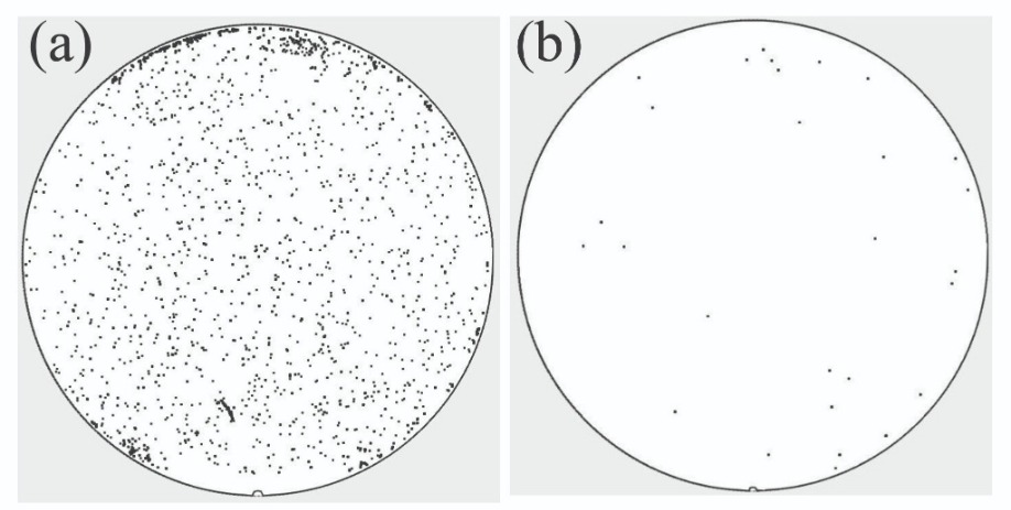
Figure 7. Defect inspection reveals the far higher particle count for 150 mm sapphire (a) than (b) 200 mm silicon. (c) The particle count of two different substrates.
One of the potential downsides with GaN-on-silicon epiwafers is cracking at the edge of the material, due to strain. However, we are able to control cracks, limiting their propagation to within 1.5 mm of the wafer edge. Note that even without any edge exclusion, the total number of cracks across the entire wafer is less than 100.
The extensive characterisation of our epiwafers highlights their great capability for making microLEDs. Armed with a wafer bow below 30 µm, an internal quantum efficiency of more than 80 percent and good wavelength uniformity, our material is well set for supporting the ramp in the manufacture of microLED displays.
Figure 8. Defect inspection highlights the high-quality of 200 mm GaN-on-silicon LED epiwafers produced by Enkris
Adopting techniques for improving the performance of the infrared laser creates powerful, reliable blue sources
BY HARALD KOENIG FROM OSRAM OPTO SEMICONDUCTORS
The laser is an ideal tool for efficient manufacturing. It is highly flexible, offers negligible changeover times, and is free from wear, thanks to its non-contact mode of operation. What’s more, improvements in laser diode performance have enabled this source to be efficient, operate either continuously or with a train of pulses that can be as short as a few femtoseconds, and provide such versatility that it can machine nearly every material.
Today, its only significant drawback is its unsuitability for processing highly reflective materials, such as gold, non-ferrous metals and particularly copper. This class of material switches from being weakly absorbing in solid form, to strongly absorbing in a liquid state, causing the melt to blow out in an uncontrollable manner. With copper, an additional issue is that it has a very high thermal conductivity, which makes it challenging to inject enough power into this material to process it. So, in short, processing highly reflective materials with infrared lasers is far from easy – and with copper it is incredibly difficult.
This issue matters, as it is a major impediment to the growth of electric-powered transportation. Manufacturers of electric vehicles need to process copper, including securely joining it to other materials and applying it as a cladding.
The solution is to reduce the wavelength of the laser. At wavelengths below 500 nm the absorption of these highly reflective materials is far higher: in copper, it is 12 times higher, and in gold it is up by a factor of 40.
However, before shorter-wavelength lasers can be used in industry, there needs to be an increase in the power produced by these sources. To realise this, our team at Osram Opto Semiconductors, working in close partnership with colleagues at Laserline, Coherent DILAS Diode Lasers and the Max Born Institute for Nonlinear Optics and Short Pulse Spectroscopy, is developing kilowatt-power direct blue lasers through a project called BlauLas, which is funded by the German Federal Ministry of Education and Research (BMBF, FKZ13N13900).
The successes that we are having will do more than just improve the capability of lasers for processing highly reflective materials. They will also support the development of blue sources for under-water materials processing, and powerful white-light sources based on the pumping of a phosphor with a short-wavelength laser.
From infrared to blue
We have no intention of re-inventing the wheel. Instead, our plan is to replicate the success of infrared laser diodes. When these are in the form of bars, they can produce a 200 W output; and when stacked together for industrial applications, they can form multi-kilowatt sources.
Today, for blue laser diodes, the commercially available sources are limited to single emitters in metal housings. These MOCVD-grown individual laser diodes, manufactured on 2-inch GaN substrates, produce just a few of watts of power in the wavelength range of 450 nm.
For the processing of copper and gold, it is far better to use a laser that emits in the blue than the infrared, due to the far higher level of absorption at these shorter wavelengths.
As a first step towards a kilowatt source, we have targeted the fabrication of a blue, 450 nm laser that continuously emits light and produces an optical output of more than 50 W when mounted on an actively cooled heat sink. To succeed, we had to ensure that the growth of epiwafers led to high-quality, homogenous epitaxial layers. This is not easy – today there exists no commercial blue-emitting laser bar on the market, due to many emitters with poor performance on the chip.
Our epiwafers, which contain as few defects as possible, have been fabricated into a range of ridge waveguide laser bars, using industry-standard chip processes. These bars, which have 23 emitters, are capable of a 98 W output when driven at 60 A. Maximum conversion efficiency is 46 percent at target operation point of 50 W.
Combining bars
To increase the output of the source, we have combined the output of several bars.
Our efforts, led by Laserline, have involved a stack of ten diode laser bars, a beam transformation system, matching optics, a focusing lens and a common fibre. With this set up it is possible to study the optical path of the laser beam from the diode facet to the optical fibre.
Osram is raising the bar for the efficiency of blue laser diodes.
This set-up welds pure copper while realising very stable heat conduction. Additional demonstrations have included the welding of gold-plated copper and fibre-reinforced plastic preforms with infrared transparency, and the joining of pure copper and steel and copper to copper.
The feasibility of kilowatt powers is clearly a breakthrough. However, this does not guarantee that the source is suitable for use in industry, which may have requirements related to the size of the source and the quality of the output. To this end, efforts led by Coherent DILAS have been directed at: decreasing the volume of the source; reducing its complexity compared with that of a single emitter; and reducing the beam parameter product, which is a figure-of-merit for the quality of the laser beam – it reveals how well the output can be focused to a small spot. Goals in this part of the project have included realising a source with a high brilliance, so it is capable of efficient coupling into a fibre with a small diameter.
Like the effort led by Laserline, bars have been used to reduce the volume of the source. The alternative – a stack of single emitters – is avoided, because it would lead to a complex, cumbersome system that is challenging to optimally align. However, for Coherent DILAS the requirements, in terms of beam-parameter product, are more challenging. The high output from the Laserline system is capable of coupling to a fibre with a high diameter, but that under development from Coherent DILAS has to couple into a small-diameter fibre high-brilliance sources at lower output power.
Coherent DILAS has much expertise in combining the output of various emitters – at the start of the project it was already capable of using this approach to produce a collimated output power of about 80 W. This power came from using integrated packages with up to 20 individual emitters, and aligning the divergent radiation from each of them with their own aspherical lens. A collimated 80 W output came from polarisation-combining two modules.
Replacing individual emitters with diode laser bars promises to lead to substantial simplification. Rather than using many lenses, just two are needed to adjust all the beams from one bar. However, to ensure success, the laser bars must be specially tuned to the beam quality of the target fibre, so that they can be combined without the need for expensive beam shaping optics. A key requirement is that, for all the emitters on a bar, the collimation of the fast and slow axis is in parallel.
Note that this approach to simplification is not a new idea. It is already used with infrared diode laser bars. Modules are made by mounting several diode laser bars with the necessary optics on a common base plate. Powerful lasers result from combining up to eight base plates in a single unit.
Our team has taken this approach with 450 nm lasers. It reaps rewards: even without additional components for symmetrizing the beam, the emission profile of the blue diode laser is good enough for efficient coupling into a common fibre. Compared with a 25 W module of individual emitters housed in standard housing – so-called TO-cans – volume is slashed by a factor of 25, while power increases from 25 W to 35 W. In addition to these gains, there is greater simplicity. Single-emitter modules require individual alignment of approximately 30 optical elements, while our tailored bar approach only needs three optical elements to be actively aligned.
We have also produced a more powerful module by mounting nine blue-emitting diode laser bars, along with collimation and stacking optics, on a common base plate. The beam quality produced by this source, which produces an output of 160 W, is good enough to efficiently couple into a 200 µm-diameter fibre.
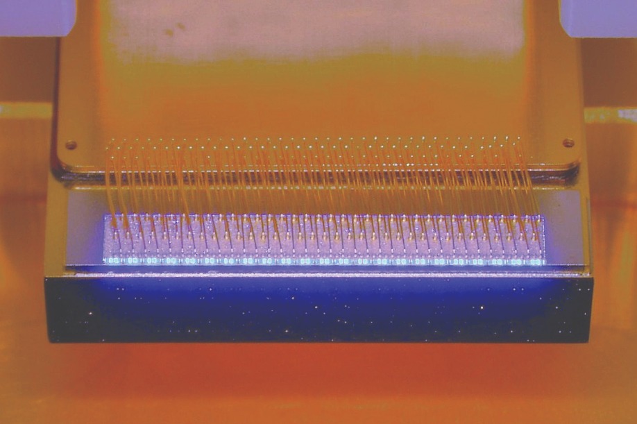
Following in the footsteps of infrared sources, a switch from a single emitter to a bar increases the total output power.
Our next step will be to combine several of these units. A source producing more than 500 W is planned by uniting the output of four 135 W tailored bars.
Ensuring lengthy, safe operation
To win deployment in industrial applications, it is essential that laser systems are reliable and can operate for many, many hours. The primary barrier to realising this is a degradation mechanism known as catastrophic optical damage, which is often fatal. Catastrophic optical damage is a generic, sudden degradation mechanism that occurs when light is locally absorbed, the temperature rises, and this is followed by further increases in absorption and temperature that spiral out of control.
Catastrophic optical damage can initiate at any absorbent point. So it may begin at either of the facets of the edge-emitting lasers, at internal defects within the waveguide, or at absorptive sites in passive waveguides. As blue sources move to a lower cost per watt, these devices will be operated at higher loads, increasing the likelihood that catastrophic optical damage will become a bigger issue in GaN-based devices.
Again, the development and long-lasting experience of the infrared lasers can come to our aid. For GaAs-based devices, there are proven techniques for reducing susceptibility to catastrophic optical damage and degradation. So, in our project we have used these approaches, such as facet coating technologies, and particular chip designs and packaging, to increase the reliability of our blue-emitting, GaN-based lasers. These efforts have paid dividends: in-depth testing by colleagues at the Max Born Institut can expose critical issues related to reliability. First long-term tests at Laserline demonstrate that these laser bars are reliable during a 12,000 hour test. Recent results show a power degradation rate of less than 3 percent per 1000 hours.
Our project is already leading to prototype commercial sources. At Welding and Cutting 2017, Laserline exhibited a demonstrator LDM 500-60 blue: it is a 450 nm blue diode laser with an output of 500 W. More success is sure to follow during our BlauLas project, including the primary goal of demonstrating 1 kW blue laser sources.
Further reading:
H. Wang et al. Optics Letters 42 2251 (2017)
H. König et al. Proc. SPIE 10514 1051402 (2018)
A. Balck et al. Proc. SPIE 10514 1051403 (2018)
Bernd Köhler et al. Proc. SPIE 10514 1051408 (2018)
Introducing an electron-shower current in an ion-implanter eliminates charge-induced damage in GaAs epiwafers
BY LAM LUU-HENDERSON, SHIBAN TIKU, MEHRAN JANANI, JOHN BONK, STEVE CANALE AND MARK BOREK FROM SKYWORKS SOLUTIONS
One of the most complex, persistent sources of yield loss in the IC industry is damage caused by electrical discharge.
Given that the silicon industry has a greater level of maturity than that of our own, it is no surprise that there is a considerable history and established methodology for addressing charging effects in silicon IC manufacturing. In those fabs, there is a potential for yield loss during the ion implantation step, commonly used to produce active devices. For certain processes, this step is carried out after the deposition of a dielectric layer, such as a gate oxide.
In addition, there may be charge-related yield loss in silicon fabs, due to the exposure of wafers to plasma treatment. During this step, which follows the formation of transistors or capacitors, damage to active and passive devices can occur due to electrical discharge accumulated during various ion bombardments.
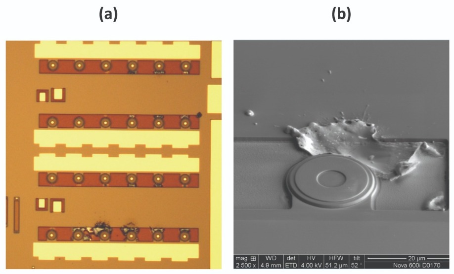
Figure 1. (a) Electrical charging defects on a pilot lot for a Skyworks HBT transistor array (b) Scanning electron microscopy image of the charging damage to the HBT structure
When processing III-Vs, a potential source of electrically induced defects is the plasma system, because it generates a high voltage on the wafer. To prevent generation of reliability impacting imperfections, proper precautions are needed to protect the wafer.
A noteworthy difference between the silicon IC industry and that of our own is that we do not employ an oxide or insulator under the gate. Consequently, electrical discharge avoidance is not common practice. In our industry, it is rare to produce ion implanted active layers – dopants tend to be introduced during the growth of epilayers. That’s not to say that ion implantation has no role to play; it is used to isolate regions of a wafer. This is normally undertaken with medium-current ion implanters, but the beam current can still exceed the limit for producing electrical damage.
Table 1. Summary of critical experimental results to determine the origin of charging defects in HBT arrays.
Device isolation in our industry is normally accomplished with the implantation of He++ or He+ ions. Due to the inherent nature of ion implantation, it is inevitable that charge build-up takes place on the wafer, despite some neutralisation of the helium beam as it traverses from its source to the target. The insulating photo resist layer and the semi-insulating nature of GaAs prevent the net positive charge, which can build up instantaneously, from adequately dissipating. This charge is an issue, as it can lead to extreme instances of electrical discharge failure.
Unfortunately, it is challenging to eliminate this charging effect on the devices on the wafer. This is particularly problematic when there are sufficient numbers of metal contacts on the wafer surface prior to ion implantation – charges can accumulate at these contacts and go beyond the threshold for electrical damage. Note that the discharge current can be so high that it can cause melting and destruction of device structures.
Figure 2. Stacked automatic inspection maps of damaged die, exposing a cross-hair and outer ring pattern with electrical discharge failures.
Pilot challenges
Several steps have been re-arranged during the development of our latest HBT process. During our evaluation of pilot lots, we observed several defects caused by severe electrical charging damage (see Figure 1). These charging-induced, blown-out defects contributed to visual and probe failures, and accounted for an overall yield loss of about 0.5 percent. Our inline automatic optical inspection tool uncovered visual defects, while functional leakage failure exposed the probe yield loss.
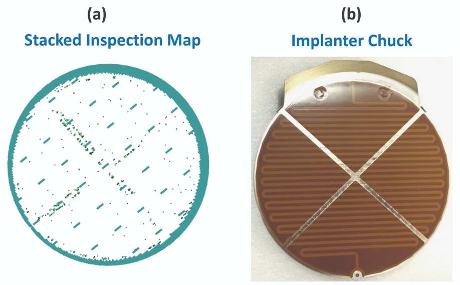
Figure 3. (a) The yield map of damaged die reveals a cross-hair pattern of electrical charging failures (b) In the Axcelis 8250 ion implanter, the electrostatic chuck ground path is in a cross and ring pattern, with the grounding pin to the left of the chuck.
Our findings, summarized in Table 1, include our observation that our wafers do not exhibit any electrical discharge damage when they are cycled through the implanter without receiving any ion implant processing. That implies that the charges generated for these defects occur during the implant process, rather than from a build-up of charge on the implanter wafer station. We also found that the higher the implant beam current, the greater the severity of charging damage; and that failures appear to be highly area dependent, impacting the larger metal features far more than smaller, isolated ones.
Another observation is that when the wafers are covered by a nitride film or photo resist, they have the most severe charging defects. Particularly susceptible to this ailment are wafers with a blanket, unpatterned sheet of photo resist. This insight reveals that it is not possible to dissipate the charges that are accumulated during the implant process, due to the combined insulating effects of the dielectric, polymer and semi-insulating GaAs substrate.
Initially, we thought that our blown and melted features, which we discovered by inline visual inspection, were distributed in a fairly random manner across the wafers. But when we stacked up the inspection yield maps, we found a very distinct cross and outer ring pattern (see Figure 2).
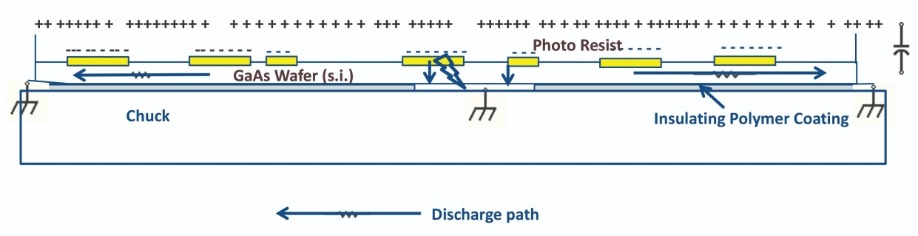
Figure 4. An illustration of the charge distribution across the wafer during implantation and the dissipation path through the grounded channels of the electrostatic chuck.
The implanter that we use is the Axcelis NV8250. The wafer station in our Axcelis NV8250 has been uniquely designed for GaAs processing, with the chuck divided into four equal quadrants so that the polarity of each of these sections can be reversed, enabling a better release of the wafer after it has been implanted. Note that the electrostatic chuck of this implanter is a modification to the original chuck offered by Axcelis. It is designed to tackle the frequent wafer breakage we faced with the original, single-outer-ring electrostatic chuck design. Prior to modification, we struggled to separate the wafer from the chuck after the implant step, due to excessive build-up of charge, which would not dissipate quickly enough to allow easy release of the wafer.
With the new chuck design, four sections are laid out in a cross configuration within the outer edge ring. With this arrangement, the entire surface of the chuck is coated with polymer, except for the aluminium cross-hair and the outer-edge ring areas – these are the only locations directly connected to ground through a grounding pin (see Figure 3(b)).
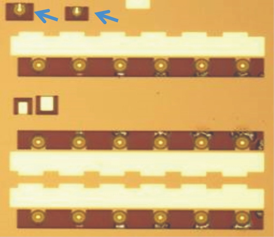
Figure 5. Electrical discharge induces damage on HBT transistor array, but the lone transistors are defect-free.
Encapsulating the metal contacts with the nitride and photoresist films prevents the accumulated charge from dissipating. Although these contacts have a lower resistance than the epitaxial layers of the HBT, the epiwafer itself is semi-insulating; consequently, the least resistive path for the release of this charge build-up is through the grounded cross and outer ring of the chuck. Due to this, the concentration of the discharge current on the wafer metal features increases along the cross pattern and outer ring areas, leading to a higher probability for electrical discharge damage in those regions.
If they are exposed, the metal features on the wafer act as antennae; and if they are covered by photoresist, they charge up like capacitors – depending on position, size and shape – until the voltage builds to a critical level, followed by a fast discharge to ground (see Figure 4 for an illustration of this failure mechanism). Note that the path of resistance depends on the position on the chuck, and is lowest in the cross and ring.
As the beam current is cranked up, there is an increase in charge accumulation on the wafer. This results in current crowding around the grounding regions during implant, and subsequently increases the number of higher electrical-discharge failures. As expected, there is a direct correlation between the magnitude of the beam current and the extent of the charging damage.
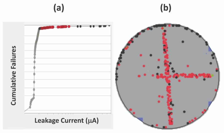
Figure 6 (a) Example of a leakage test detecting electrostatic damage failures. (b) A yield map showing failed dies in a cross and ring pattern.
Note that with product wafers, it is most common for the metal features to be under photoresist, and the remaining open field areas to be covered and implanted. However, in extreme cases, the whole wafer can be covered by photoresist, causing an aggressive build-up of charge, followed by catastrophic electrical charging failures.
To effectively identify these discharge failures, we have employed two modes of detection: automatic optical inspection, first after the implant step and again at the final outgoing die inspection; and a leakage probe test. The latter employs tighter limits to catch electrically weakened die that threaten to go undetected by automatic optical inspection and could potentially result in escapes. To identify these marginal and leaky die, we increased the bias voltage (see Figure 6 for the results of this approach).
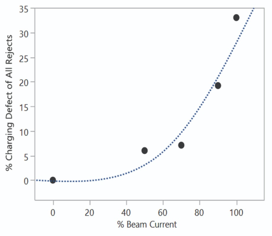
Figure 7. Charging induced defects increase as the implanter beam current rises.
We live in an era of lean manufacturing, where it is often unfeasible to modify hardware for defects occurring at a level of parts per million. In these circumstances, alternative approaches are required to mitigate and contain these types of yield loss. One option is to dial back the implant beam current to limit the rate at which the ions hit the wafer. Ultimately, this decreases the charge collected at the contact metal, and should diminish the level of damage (see Figure 7).
To put this theory to the test, we varied the implant beam current from 0 percent to 100 percent, before immediately scrutinising implanted wafers with automatic optical inspection. After comparing the number of charging-induced failures with the total for detected defects, we observed a strong correlation between the beam current and the amount of charging damage.
Back in the 1980s, Eaton Corporation thoroughly studied and documented the role played by the implant current on the degree of charging on the wafer. They drew the same conclusion: reducing the implant current offers a quick, simple containment method for reducing the number of charging-induced failures. However, this undoubtedly comes at the expense of reductions in throughput and overall efficiency.
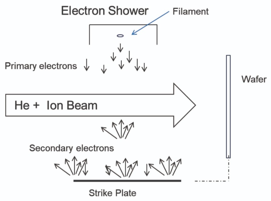
Figure 8. Charge-induced defects fall with the introduction of an electron shower into the end station, which features a single filament configuration. The strike plate is made of graphite to avoid contamination to GaAs circuits.
InAir transfer robot for the Axcelis NV8250.Source: Axcelis Technologies
Operator Interface and Load Station for the Axcelis 8250.Source: Axcelis Technologies
This concept will be familiar to anyone that’s aware of the ‘antenna’ rules applied to the processing of silicon ICs. The basic principle is that the area of the wafer covered by a resist should not exceed a certain threshold. However, this can be hard to accomplish when undertaking isolation of some circuits, such as the HBT power array. In this case, the entire array can be 100 microns or more in length, but covered by a photoresist as a single entity, since electrically it is just a single device.
One way to comply with these rules is to configure the transistor collector contacts in the array so that they are just segmented electrically (see Figure 5). This ensures that each contact has a smaller conducting surface. Joining the contact areas together with an interconnect metal, deposited after the ion–implant step, trims charge build-up and reduces the likelihood of arcing-related events.
Showering with electrons
Out of all the options for addressing implant-generated charging defects, the most dependable and recommended is the industry-tested electron shower. Originally developed by Eaton Corporation, it has been widely adopted in the silicon industry.
In the case of our Axcelis NV8250 ion implanter, the electron-shower is integrated into the end station, where the wafer is staged for implantation. Using this design, electrons from the emitting filament flood the ion beam with a surge of negative charge, neutralizing positive He+ and He++ ions prior to implantation (see Figure 8).
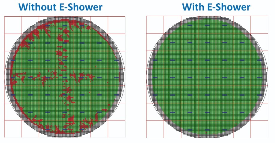
Figure 9. Yield maps of wafers with and without electron-shower during isolation implant.
Many high-volume, high-density IC fabs use tools with electron showers. It is a dependable technology, but there are risks, as there is the possibility of having charging defects from a negative potential. So, to avoid inducing discharge damage created from an overdose of negative charges, careful process development is essential when optimizing electron-shower settings. Engineers must tread a fine line between ensuring neutralization and preventing excessive negative charges.
To determine the optimal electron-shower settings, we performed a ‘design of experiments’. This involved GaAs wafers deposited with contact metal and coated with SiN, and also wafers with an unpatterned isolation photoresist, which provides an extreme condition for assessing the degree of charging damage. Both types of wafer were implanted with and without an electron-shower beam. Experiments revealed that wafers processed with an electron-shower were free from charging symptoms, while those without an electron shower exhibited a severe case of discharge damage (see Figure 9).
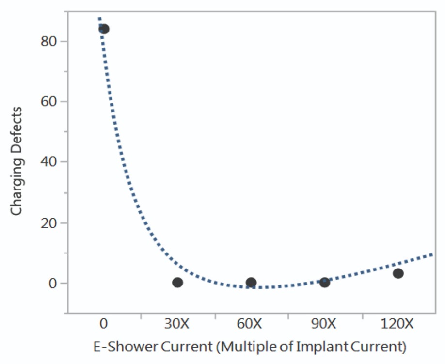
Figure 10. The charging-induced defect percentage as a function of electron-shower primary beam current, for a given implant recipe.
It is recommended that the electron-shower primary current should be around thirty times the implant beam current. We have put this figure to the test, finding that even when the current is increased well beyond this recommended value, there is still zero to negligible implant charging-induced defects (see Figure 10). In other words, there is a very broad process window for using the Axcelis NV8250, while realizing an extremely low probability of negative charging.
By undertaking several iterations of our design-of-experiment, we have determined the ideal electron-shower process conditions for the Axcelis NV8250 implanter. In turn, this has led to improvements in optimal isolation and cycle times, as well as a major improvement to the electrical charging yield loss.
Our work shows that electrical charging and its consequent damages are not limited to the silicon IC industry, but extend to the makers of ICs based on
III-Vs. Charging can occur in all process steps involving plasma or charge beams. In particular, failures can be traced back to the ion implantation step used during the isolation process, which has the potential to produce heavy, visible damage to metal features. If the order of processing is changed, or there is a modification to process steps that involve charge species, there is the threat that this new routine creates visible or optically undetectable defects.
In our case, our new process flow has involved covering semi-insulating wafers, which have existing metal features, with insulating SiN and photoresist, prior to an ion-implantation step. Unfortunately, this combination creates the ideal condition for a catastrophic electrical discharge yield event. To get to the bottom of this issue, and ultimately determine the best way forward, we undertook a detailed assessment of these implant induced failures, followed by thorough experimental analysis. The discoveries that followed have enabled us to uncover the primary failure mechanism, and unlocked the door to critical preventive methods, proper quality control measures and overall improvement to product yield and reliability.

The MOCVD growth of heterostructures incorporating the E-type polymorph of gallium oxide could open the door to devices combining an ultra-high bandgap with a high carrier mobility
Researchers at Sun Yat-Sen University, China, are claiming to be the first to grow high-quality layers of e-type Ga2O3 on a sapphire substrate.
Their efforts could aid the development of power devices that combine tremendous levels of efficiency, thanks to an ultra-wide bandgap of typically 4.9 eV, with low cost, due to growth on a relatively cheap substrate.
For some forms of Ga2O3, such as the b-type, the highly anisotropic lattice structure dictates that a native substrate of the matching polytype is used for the growth of epilayers. That restriction is far from ideal, according to team spokesman Zimin Chen, because the cost of this form of gallium oxide substrate is around one hundred times higher than that of sapphire or silicon.
“Even though the cost of the beta gallium oxide substrate should decrease in future, we do not think that it could become as cheap as sapphire or silicon,” argues Chen.
However, it’s not just the high cost that is discouraging the use of the Ga2O3 substrate. It’s also small in size, holding back economies of scale, and is hampered by a poor thermal conductivity.
With sapphire and silicon, the merits of the substrate extend beyond its widespread availability, low-cost, and large diameter. It also has the potential to address the low room-temperature carrier mobility of Ga2O3 – it is typically below 150 cm2 V-1 s-1.
The promising solution, which follows in the footsteps of the evolution of GaN, is to exploit the pronounced polarization effect in the e-type polymorph of Ga2O3. To do that, there is a need to form heterostructures with a two-dimensional electron gas.
“This is why we are more interested in e-Ga2O3, rather than a-Ga2O3 or b-Ga2O3,” explains Chen.
Ultimately, Chen and co-workers want to grow e-Ga2O3 on silicon. That’s not easy, because this ultra-wide bandgap material must be grown at high-temperatures under oxygen or water, conditions that could easily oxidise the silicon surface.
Due to this pitfall, the team have started with growth on sapphire. Double-polished c-plane substrates are loaded into an MOCVD reactor equipped with triethylgallium and deionised water precursors. Then, using argon as a carrier gas, heterostructures are formed by growing a 15 nm-thick e-Ga2O3 nucleation layer at 600 °C, followed by a 200 nm-thick layer of this oxide at 640 °C.
Scrutinising this film with cross-sectional transmission electron microscopy exposes the interfaces between sapphire and the nucleation layer, and the nucleation layer and the epilayer. This technique also reveals that the interface between the nucleation layer and the epilayer is rough, due to the three-dimensional growth mode. However, as growth proceeds after this interface, the film flattens, indicating a switch to the two-dimensional growth mode.
The team have studied the surface of their samples by atomic force microscopy. This reveals steps and terraces, indicative of layer-by-layer growth. Non-even distribution of the steps is attributed to a distortion caused by pinholes, which result from the significant lattice mismatch between the substrate and the epilayer.
X-ray diffraction offers an insight into the density of screw dislocations, with values from the rocking curve suggesting a density of 1.8 x 108 cm-2. Meanwhile, optical absorption measurements indicate a bandgap of 4.9 eV.
Chen says that the next steps for the team are to try and demonstrate heteroepitaxy of high-quality e-Ga2O3 on silicon (111) and to produce high-quality heterostructures from e-(AlGa)2O3 and e-Ga2O3.
Reference
Z. Chen et al. Appl. Phys. Express 11 101101 (2018)
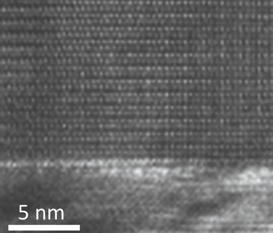
Cross-sectional transmission electron microscopy reveals the three-dimensional growth mode in the nucleation layer and the two-dimensional growth mode in the epilayer.
When high-order gratings are formed along the sidewalls of the ridge, GaN lasers can produce a high side-mode suppression ratio
Low spectral purity is preventing the GaN laser diode from providing a source of emission for laser-cooling, a technology used to improve the performance of atomic clocks.
But this could now change, thanks to the development of a novel GaN laser with a very high side-mode suppression ratio.
This device, produced by a team from the UK and Poland, realises a high spectral purity by incorporating high-order notched gratings into a distributed feedback laser.
Turning to gratings to ensure single-wavelength emission in a GaN-based laser is not a new idea. However, conventional approaches run into difficulties. If buried gratings are employed, they require complex overgrowth steps that can introduce defects; and if surface gratings are used, this can compromise the quality of the p-type contact, and increase optical losses in electrically unpumped grating regions.
A far better approach, according to the team from the UK and Poland, is to form the gratings along the sidewalls of a ridge-waveguide laser.
Merits of this architecture are that the sidewall grating can be designed and implemented postgrowth, after the emission wavelength is known; and there is greater design freedom, because the coupling coefficient is determined by the planar layout of the grating, rather than the etch depth.
The GaN laser produced by the team has a high-order distributed-feedback design, known to provide an intrinsically narrow line-width in InP lasers. With GaN, implementing the design is more challenging, as the reflection bandwidth must be far narrower.
To determine the design of the GaN laser, the team turned to a transmission matrix method to estimate the number of notched pairs. This suggested that a 39th order grating with 125 notch pairs along the ridge would lead to a bandwidth of about 0.1 nm.
Lasers were formed by processing epiwafers containing Al0.06Ga0.94N cladding layers and three InGaN quantum wells sandwiched between GaN barriers. A Raith VB6 electron-beam lithography system with a write resolution of 1 nm defined the ridge and grating patterns.
Using a 120 nm-thick SiO2 mask, the researchers etched smooth, vertical structures into the ridge using an optimised, inductively coupled plasma etching process. After this, the team deposited a SiO2 layer to insulate metal contact pads from the semiconducting layers, added metal contacts, and cleaved the wafer into individual chips, which were mounted in TO cans.
Testing these laser chips revealed a threshold current of 130 mA, a slope efficiency of 0.27 W/A, a side-mode suppression ratio of 35 dB, and a continuous-wave output power of 20 mW. According to team spokesman Thomas Slight from CST Global, these performance figures should be good enough to use this laser for the cooling of Sr+ atomic clocks.
The team also processed Fabry-Pérot lasers from the same wafer. They had an efficiency that is more than double that of the lasers with the sidewall grating, and a threshold current that is lower by more than a factor of two.
“We think big improvements can be made by optimising the grating design and using facet coatings,” says Slight.
With these steps, the efficiency of the Fabry-Pérot laser will still be a little bit higher, but that will not be an issue for the cooling of Sr+ atomic clocks. “Maybe in a miniature portable device it would become a consideration,” reasoned Slight, “but even then the power consumption wouldn’t be much increased.”
The next goal for the team is to measure the linewidth of its laser. “This is key, as it must be less than one megahertz for use as the cooling laser in the strontium-ion clock,” says Slight.
Reference
T. Slight et al. Appl. Phys. Express 11 112701 (2018)
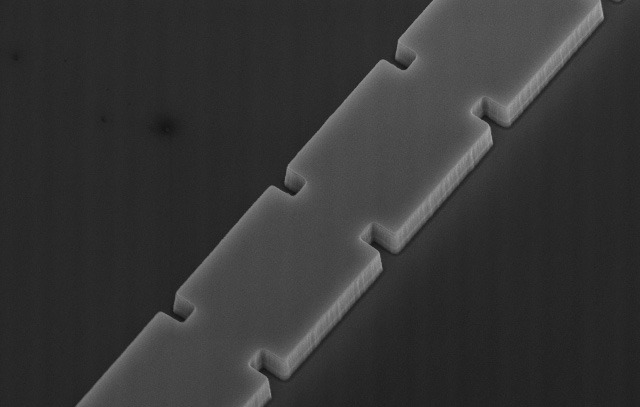
A high-quality, high-order grating formed by inductively coupled plasma etching holds the key to the very high side-mode suppression ratio of the GaN laser.
Record-breaking output powers are realised by doubling the cavity length of the GaN VCSEL
Engineers at Stanley Electric and Meijo University, Japan, are claiming to have set a new record for the output power of the blue VCSEL. The team’s device produces a CW output of more than 15 mW at room-temperature, and 2.7 mW at 110 °C.
The capability to operate at high temperatures makes this VCSEL a promising candidate for deployment in car headlights, according to corresponding author Masaru Kuramoto, an engineer at Stanley’s R&D Labs.
“Stanley Electric currently produces automotive headlamps using LED white light sources,” says Kuramoto, “and we expect that the blue VCSEL will be used for next-generation laser headlamps.”
He believes that there are many reasons why the VCSEL is an ideal source light for headlamps: it is not plagued by catastrophic optical damage; it emits a circular beam with limited divergence; it has a small temperature dependence on the lasing wavelength; and it can form two-dimensional arrays.
To realise the record-breaking output power, Kuramoto and co-workers trimmed the thermal resistance of the VCSEL by lengthening its optical cavity.
Additional features are a low internal loss and a low reflectivity for the front mirror. These refinements, reported earlier this year, raised the bar for the peak output power from this class of device to its previous record of 6 mW.
The latest design has an optical cavity length of 10l, which is twice that of its forerunner.
There is no point in increasing the cavity beyond this, argues Kuramoto. Go down this path and thermal resistance fails to improve, while slope efficiency and threshold current are impaired, due to higher diffraction loss and a reduction in optical confinement, respectively.
Fabrication of the team’s VCSEL began by loading a GaN substrate into an MOCVD reactor and growing a distributed Bragg reflector with 42 layers of AlIN, interleaved with 41 layers of GaN, and then a 10l cavity. This cavity contained a 1.57 mm-thick layer of n-GaN, an active region with five quantum wells, a p-AlGaN electron-blocking layer and a layer of p-GaN. To benchmark results, the team also produced a variant with a 5l cavity that only differed in the thickness of its n-GaN: in this case, 660 nm.
Reactive-ion etching into the p-GaN to a depth of 20 nm defined the circular apertures for the devices, prior to the deposition and lift-off of a 20 nm-thick film of SiO2 with a self-aligned process. Fabrication finished with: the deposition of an indium tin oxide layer, a Nb2O5 spacer layer, and a 10.5-pair distributed Bragg reflector made from the pairing of SiO2 and Nb2O5; the addition of n-type and p-type electrodes; and the coating of the back surface of the substrate with an anti-reflection coating, formed from the pairing of SiO2 and Nb2O5.
Measurements on devices mounted p-side down on a copper heatsink revealed that the VCSEL with the 10l cavity had an output power of 15.7 mW at 20 °C, a threshold current of 4.5 mA, and a threshold voltage of 5.1 kV. In comparison, the variant with the 5l cavity had an output power of 8.2 mW at 20 °C, a threshold current of 4.2 mA, and a threshold voltage of 5.1 V.
Thermal rollover limits the optical output of both devices. This impediment leads to a peak output at 20 mA for the VCSEL with the 5l cavity, while the 10l-variant produces its maximum at 29 mA.
Kuramoto believes that the team’s refinements to its lasers, such as the reduction in thermal resistance, could also be applied to green VCSELs.
“The internal-loss reduction by introducing the silicon dioxide, buried lateral index guide, will lead to superior performance, such as low threshold and high efficiency, even in the green VCSEL,” says Kuramoto.
Plans for the future include the fabrication of a VCSEL that combines single transverse-mode operation with a high output power, and the construction of arrays delivering a high output power.
Reference
M. Kuramoto et al. Appl. Phys. Express 11 112101 (2018)
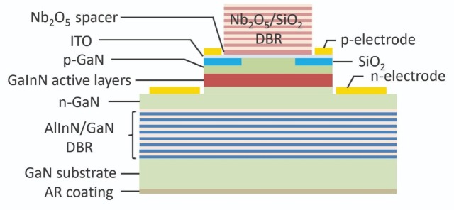
A record output power for a blue VCSEL resulted from lengthening the cavity, while trimming optical loss and reducing the reflectivity of the front mirror.