


Advances in optical communications are at the heart of every ECOC gathering, with this year’s conference taking place 23-27 September in Rome. ECOC once again addressed the width and breadth of the industry from its most advanced research to practical demonstrations of next-generation optical circuit design, fabrication and photonic integration. If your company unveiled a new device, technique, or integration advances at ECOC, share your insights with PIC Magazine readers—our next editorial deadline is 16th November.
A hot topic at ECOC was the impact of coherent optical technologies, with 400G transceivers garnering the most attention. Coherent Solutions, MultiLane and National Instruments demonstrated their combined transceiver PXI test platform for pluggable devices. A 100G transceiver was on the test bed, but according to visitors, the companies stated their approach would scale for 400G—a single solution applicable from design to the production floor.
Elsewhere in Coherent Land, NeoPhotonics discussed its success with 64 Gbaud optical solutions, while there were multiple 100G / 200G transceiver demos. The IEEE is developing a new task force that will explore taking high-speed Ethernet beyond 10 km, with smart money betting that coherent optics will play a role. IEEE’s ultimate view on coherence will likely influence the future shape of data center interconnects and potentially create opportunities for PICs.
Other hot topics at ECOC included interoperability and speculation over roles that optical technologies might/could/will play supporting 5G rollouts. Most saw possibilities for 25G/100G transceivers as well as photonic integrated circuits (PICs) for front-end requirements. While this was discussed in Rome, two US telecom Tier One’s (AT&T and Verizon) were promoting their 5G systems in select cities. Both are using proprietary approaches to achieve 350-1000MB downloads. ECOC exhibitors foresaw opportunities for 100G transceivers in super MIMO antennas, but with so few retail 5G services now available, expect no ‘one-size-fits-all’ consensus anytime soon.
Multi-source agreement (MSA) announcements were another ECOC staple along the Road to Rome. Attendees noted that demonstrations hosted by the 100G Lambda MSA and COBO were highlights, and that multiple testing vendors offered excellent examples of 400G hardware and methodologies. The Ethernet Alliance booth saw several 400G MSAs represented.
In this edition of PIC Magazine we delve into scaling indium phosphide (InP) for PICs from authors at Eindhoven University of Technology. We also dive into automating test, assembly and packaging courtesy of Physik Instrumente (PI), and new PDK support from VPIphotonics. We also look at the ability to add micro-optic structures through advanced 3D micro-printing by Nanoscribe, and have an excellent series of updates from EPIC by Ana Gonzalez and Jose Pozo.
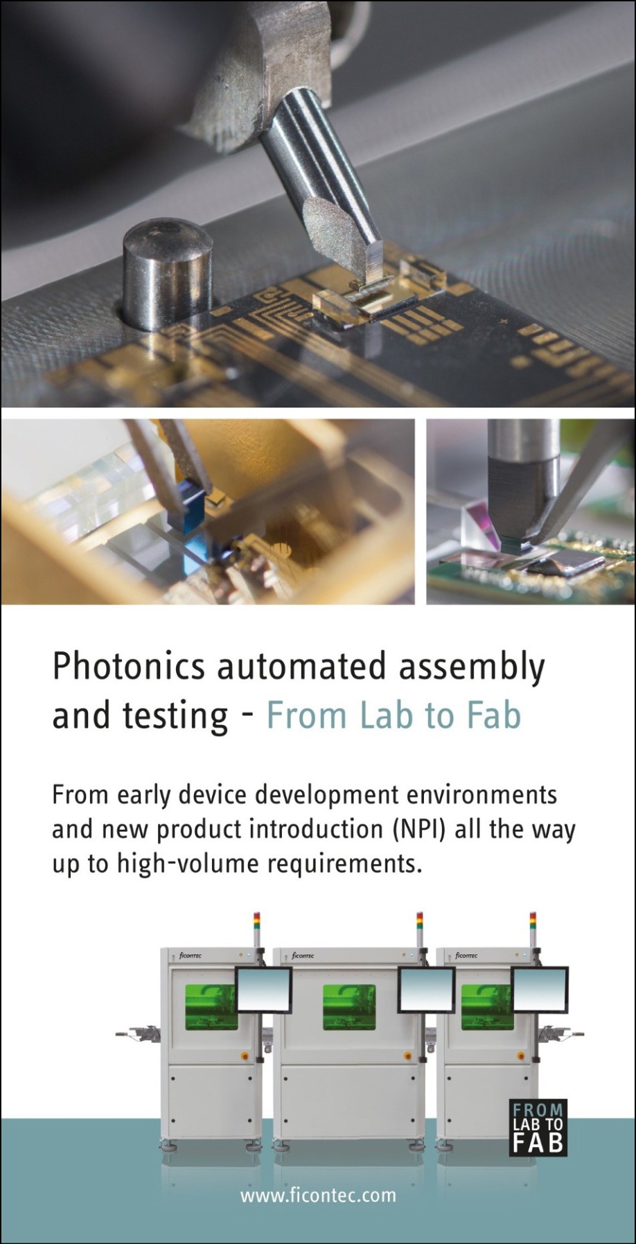
ficonTEC Service GmbH has announced a comprehensive modernization of the company’s product strategy. The new approach allows ficonTEC to properly address increasing customer focus on in-line production line applications, while at the same time retaining continuity for existing customers, commitments and projects with current stand-alone machines.
Initially, new ASSEMBLY machine systems, utilizing a newly-designed housing format and state-of-the-art feed-in/out capabilities, will be offered in specific ‘in-line’ configurations for production line applications. The new machine format can be supplied either individually as a versatile production cell designed to slot into an existing or proposed production line, or as task-optimized machine segments comprising several different systems.
Looking forward, the new housing format is already compatible with other ficonTEC assembly and production machine types and can additionally be offered both as stand-alone and in-line machine systems.
Importantly, for customers and key activities requiring continuity with previous systems, the entire range of current machine systems – including ASSEMBLY, FIBER, BOND, CUSTOM, TEST, INSPECTION and STACK– will continue to be available indefinitely. All stand-alone products remain custom configurable with ficonTEC’s proprietary assembly and test modules.
While retaining all of the popular customer-oriented features of ficonTEC’s existing stand-alone products, the new in-line machine systems additionally provide much improved support for high-volume production requirements, for example, those associated with the highly visible transition to integrated photonics approaches for component manufacturing.
ficonTEC’s easy-to-use but nonetheless sophisticated process control software will continue to tie everything together, providing a consistent look & feel across all products –both old and new.
SMART Photonics have completed another equity investment round. SMART Photonics is a European manufacturer of InP Photonics components with production and research facilities located in Eindhoven, The Netherlands. SMART Photonics offers production and development portfolio of generic technology as well as engineered custom processes. The production services range from epitaxial growth and regrowth to coating and testing of the individual chips.
SMART Photonics accommodates both proof-of-concept and volume manufacturing. The generic integration process is specifically designed to provide short turn-around time and low-cost prototyping and volume manufacturing for photonic integrated circuits.
CFO Robert Feelders: “We collected another € 6 million, mainly from informal investors. Besides this new investment, the majority of our existing informal investors converted their loans into shares (€ 4,5 million), which strengthens our financial position even more. This expresses great confidence in our potential and growth. With this new funding, we will be able to improve both the stability and robustness of our processes, which will lay a firm foundation in making the next step towards a full production plant.”

Mentor, a Siemens business, has announced LightSuite Photonic Compiler – the industry's first integrated photonic automated layout system. This new tool enables companies designing integrated photonic layouts to describe designs in the Python language, from which the tool then automatically generates designs ready for fabrication. The resulting design is "Correct by Calibre" – with the implementation precisely guided by Mentor's Calibre® RealTime Custom verification tool. LightSuite Photonic Compiler enables designers to generate as well as update large photonic layouts in minutes versus weeks.
With this breakthrough technology, companies can dramatically speed the development of integrated photonic designs that will bring speed-of-light communications directly into high-speed networking and high-performance computing (HPC) systems. It also speeds the development of more cost-effective LiDAR technology, which is seen as essential to enabling the mass deployment of autonomous vehicles.
"Mentor's LightSuite Photonic Compiler represents a quantum leap in automating what has up to now been a highly manual, full-custom process that required deep knowledge of photonics as well as electronics," said Joe Sawicki, vice president and general manager of the Design-to-Silicon Division at Mentor, a Siemens business. "With the new LightSuite Photonic Compiler, Mentor is enabling more companies to push the envelope in creating integrated photonic designs."
"LightSuite Photonic Compiler fixes the biggest roadblocks preventing industry-wide adoption of electro-optical design and simulation of photonic chips," said M. Ashkan Seyedi, Ph.D., senior research scientist, Hewlett Packard Enterprise. "Photonic chips promise amazing performance, but designing circuits today is just too difficult and requires specialized knowledge. LightSuite Photonic Compiler circumvents those challenges and enables scalability. I'm thrilled to have worked with Mentor to develop this tool to make it possible for anyone to design and build photonic circuits as easily as designing electronic circuits."
Until now, photonic designers have been forced to use analog, full-custom IC tools to create photonic designs. In this flow, designers manually place components from a process design kit (PDK) and then interconnect those components manually. Photonic components must be interconnected with curved waveguides. After they have manually placed and interconnected the components, they typically perform a full Calibre physical verification run to check for design rule violations, as Calibre DRC can find violations even in photonic designs.
Mentor designed the new LightSuite Photonic Compiler specifically for photonic layout so that engineers have complete control of their layouts and can use the tool to automatically perform the placement and interconnecting of both photonic and electrical components. The designers create a Python script that is used to drive the LightSuite Photonic Compiler. Initial placement can also be defined in Python, or come from a pre-placed OpenAccess design. Next, the tool interconnects photonics components with curved wave guides. As some of the components might contain built-in electrical elements, the tool will route these electrical connections simultaneously along with the curved waveguides.
LightSuite Photonic Compiler uses Calibre RealTime Custom during the inner placement and routing loop, resulting in a layout that is design-rule correct. The tool enables designers to perform "what-if" design exploration for photonics designs, which was prohibitively time consuming with manual layout. With this new level of automation, designers can generate a new layout in minutes versus weeks for large designs.

Silicon photonics is held back by the lack of a suitable monolithic light source. The solution: introduce lasers, waveguides and photodetectors that are formed from arrays of nitride nanowires with InGaN disks by Pallab Bhattacharya and Arnab Hazari from the University of Michigan
Throughout the twentieth century, engineers improved the performance of the silicon IC by simply reducing the size of the transistors. But in recent times, progress has been far harder to come by. It has hinged on the introduction of exotic materials and architectures to ensure that the miniaturisation of the transistor does not produce dire consequences – and it will not be long before there is a need to add light-based communication, to enable faster transfer of information within and between CMOS chips.
The latter technology, often referred to as silicon photonics, has much promise, because light travels far faster than electrons (see Figure 1 for an example of a simple photonic circuit). Due to this hike in speed, circuits that incorporate photonics can operate at far higher communication rates than their electronic cousins, shortening on-chip and off-chip delays.
Fulfilling the promise of the optically equipped IC is not easy, however. Silicon will undoubtedly remain the material for the electronics, but its indirect bandgap hampers its use in the components needed for optical communication. While impressive progress has been made in research and commercial development of silicon-based detectors, modulators and passive waveguides, III-Vs are the essential ingredient for making a light source.
The current solution is to bond either GaAs-based or InP-based lasers to the silicon wafer. That’s not ideal, though, because it creates thermal issues: the silicon gets hot, pegging back laser output and efficiency. A far better approach is the epitaxial growth and fabrication of a diode laser on silicon. Ideally, this source must emit at around 1.3 μm, the zerodispersion wavelength for the SiO2 waveguide. Note that another advantage of this spectral range is that it is in the regime of eye-safe operation.
Unfortunately, success with this approach is hampered on three fronts: there is a large lattice mismatch, giving rise to a high density of dislocations; there is a thermal expansion coefficient mismatch that can cause strain in the device; and there is the potential for unwanted antiphase domains, which can be created during the growth due to the polar/non-polar nature of the epitaxial layers and the substrate.
Despite all these drawbacks, encouraging progress has been made by using devices that sport suitable buffer layers. At the University of Michigan, we have led the way, demonstrating the first InAs/GaAs quantum dot laser that is grown directly on silicon. And other groups are now following in our footsteps, improving the performance of this device on (001) silicon substrates.
However, progress is slow, and problems remain. The silicon that’s used as a foundation for the lasers is offcut at 4° towards the (011) direction in order to avoid anti-phase domains and resulting defects.
Meanwhile, CMOS circuits are formed on (001), a situation that’s not going to change. In addition, fabrication of the lasers involves the growth of complicated buffers and intermediate layers, making the whole process cumbersome.
Switching to nitrides
Our view is that instead of trying to address all of these problems, it is far better to switch to another material system. We chose the nitrides, because they combine tremendous tunability of the bandgap with growth on a variety of substrates, such as sapphire, SiC and silicon – including the form that’s used for CMOS circuits.
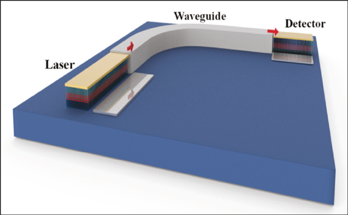
Figure 1. The simplest example of a photonic integrated circuit on a silicon platform. At the University of Michigan, diode lasers and photodiodes are fabricated with III-nitride heterostructure disk-in-nanowire arrays grown directly on silicon by MBE. The waveguide is formed by dielectric deposition.
One distinguishing feature of GaN and its related alloys is its large, intrinsic polarisation. The fields that result aid the design of HEMTs, but are a drawback to LEDs, hampering radiative recombination efficiency and limiting the thickness of the quantum well. A further complication is that increasing the indium content of an InGaN well to propel its emission from the blue to the green creates compositional inhomogeneities. This makes it very challenging to produce light sources with acceptable efficiency beyond the blue. And magnifying this issue is the high density of defects, arising from the substantial lattice mismatch with the substrate.
To sidestep these issues, we are avoiding planar III-nitride semiconductors, and instead working with nanowires. Arrays of these nanowires can be grown directly, without masks or catalysts, on various substrates including CMOS-compatible (001) silicon. The density of the nanowires in these selforganized random arrays may range from 108 cm-2 to 1011 cm-2, and their diameter can be between 20 nm and 80 nm (see Figure 2).
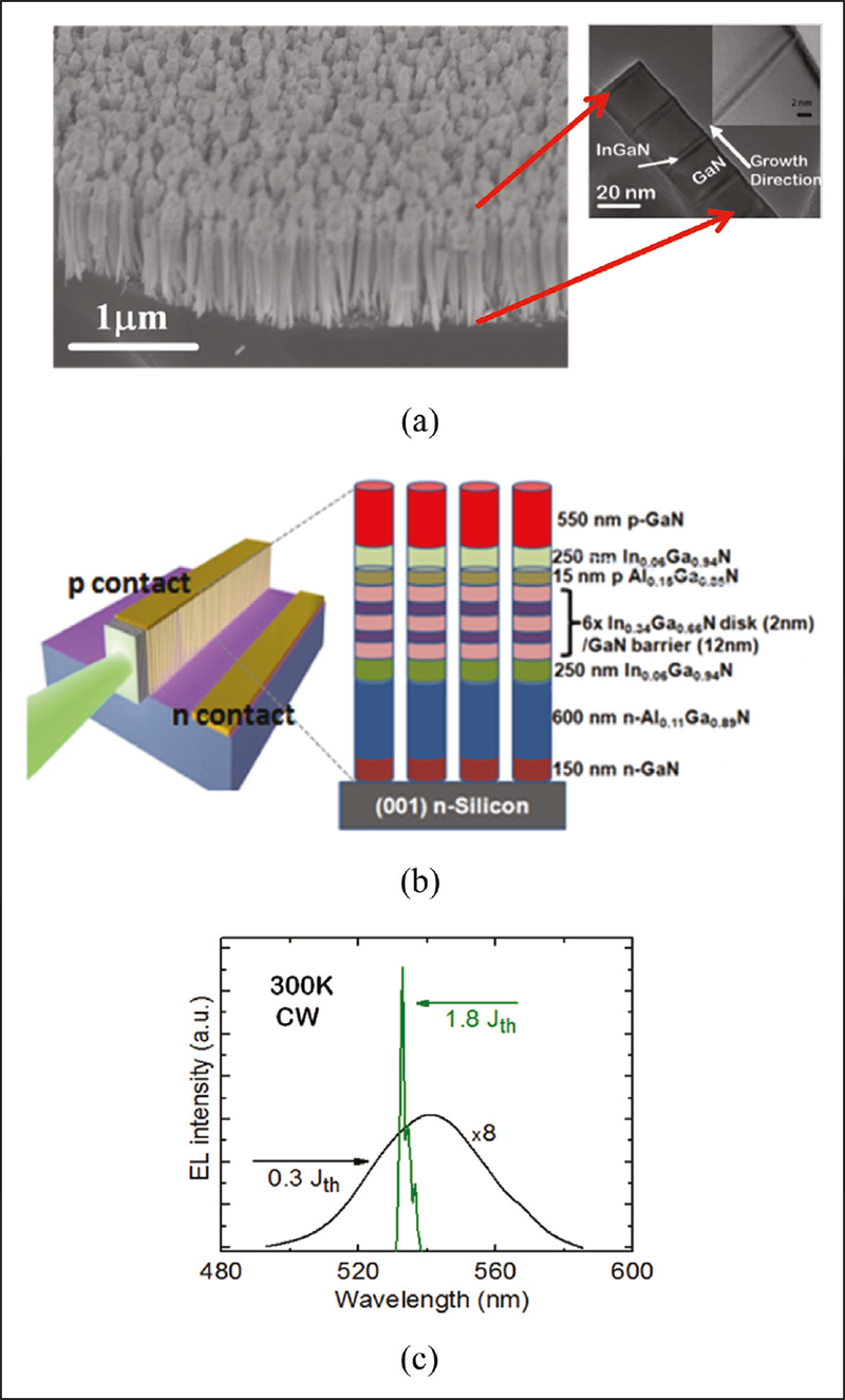
Figure 2. (a) Scanning electron microscopy and high-resolution transmission electron microscopy images of a disk-in-nanowire array on silicon; (b) an illustration of a disk-in-nanowire edge-emitting diode laser; (c) output emission characteristics of a green-emitting laser below and above threshold injection.
Issues related to high polarisation fields are greatly diminished in these wires, thanks to radial relaxation of strain during epitaxial growth. The nanowires also suppress extended defects, thanks to the larger surface-to-volume ratio; and emission can span a far wider spectral range through the insertion of lower bandgap disks, such as those made from InGaN, into larger bandgap GaN or AlGaN nanowires. Note that emission from the structure may be tuned by tweaking the composition of single or multiple disks.
Another benefit of the nanowires, which we realised soon after embarking on this effort, is that the indium incorporation in the InGaN disks can be far higher than it is in planar quantum wells, without any adverse effects. And we can realise quantum efficiencies of more than 50 percent.
We have used these disk-in-nanowire arrays to produce green- and red-emitting LEDs – and more importantly, diode lasers for the first time. Note that our edge-emitting nanowire array lasers (see Figure 2) appear exactly like planar devices after fabrication on the (001) silicon substrate. To realise emission in the green and red, the InGaN disks that form the active (gain) media within the GaN waveguide and AlGaN cladding have an indium content of 34 percent for 534 nm emission, and 51 percent for 630 nm emission.
Hallmarks of these emitters include the absence of reflections, scattering and distributed feedback, due to the wavelength associated with the emission being far larger than the diameter of the nanowire (the polymer parylene surrounds the wires, creating a structure that behaves as a composite medium with a refractive index of 2.1). Characteristics associated with photonic crystals are also avoided, due to the randomness of the array.
Typical output powers for these lasers are 10 - 15 mW. The threshold current densities are fairly insensitive to temperature variations (To >200K), and have a typical value of about 1 kA cm-2. Electrical modulation indicates that the modulation bandwidths reach 3 GHz without implementing any special designs to the nanowire heterostructures.
Realising the near-infrared
To propel the emission of our lasers from the visible to the near-infrared we have had to crank up the indium content in the InGaN disks. Following careful optimization of the MBE parameters, metal fluxes and growth temperature, we have incorporated multiple In0.85Ga0.15N disks in our GaN nanowires. Encouragingly, these structures produced strong, room-temperature photoluminescence at the desired wavelengths. We are thankful for the assistance of Millunchick’s research group at the University of Michigan – they offered an insight into the quality of our nanowires, by undertaking detailed imaging with a transmission electron microscope.
We have fabricated lasers from these heterostructure nanowire wafers at our university’s Lurie Nanofabrication Facility. Production of the devices involved a series of steps that included photolithography, etching, metal deposition, planarization and the addition of the polymer parylene. Fabrication is not easy, because rough laser facets that result from dicing the nanowire array/parylene composite reduce reflectivity to such an extent that it prevents the necessary cavity feedback. To overcome this, we smooth the facets with focused ion beam etching. A further enhancement to facet reflectivity comes from the addition of multiple periods of ZnSe and MgF2, which together form a distributed Bragg reflector. This enables a hike in reflectivity to around 90 percent, and ultimately the fabrication of lasers with an emission peak of 1.2 μm and a room-temperature output of around 7 mW. These first-of-a-kind, nearinfrared, III-nitride-based diode lasers are transparent to silicon, thereby making it possible to realize low loss photonic circuits monolithically on silicon.
In these devices, there is a large polarisation field, revealed by the blueshift between the electroluminescence peak below threshold and the coherent lasing peak above threshold. Nonetheless, these fields are far smaller than those in planar quantum wells.
Other encouraging attributes of these lasers are: the absence of any significant material segregation in the active disks; a low threshold current; a high degree of temperature stability of the threshold current (T0 >200K); a high differential gain; and good modal characteristics.
In our quest to realise a laser emitting at 1.3 μm – the sweet spot for silicon photonics – our only remaining option to red-shift the emission was to attempt to incorporate binary InN disks in the GaN nanowires. This is a far better approach than forming thicker InN regions along wires, because the disks provide quantum confinement, and tend to have a lower dislocation density.
Epitaxial growth of InN disks is far from easy. It is critical to determine the optimum growth temperature, which was an unknown parameter. We were also hampered by the low sticking coefficient of indium. If we selected too high a substrate temperature, this would enhance indium desorption; and if we chose too low a value, the heterostructure would be plagued by poor crystalline quality and defects. Following some optimisation, we selected a substrate temperature of 489°C.
We were delighted to discover that our InN/GaN disk-in-nanowire arrays could produce strong photoluminescence and a high radiative efficiency. The latter is 67 percent, a value exceeding that for ternary InGaN disks of all alloy compositions, before or after passivation with parylene. Photoluminescence intensity peaks at 1.6 μm, an extremely encouraging result.
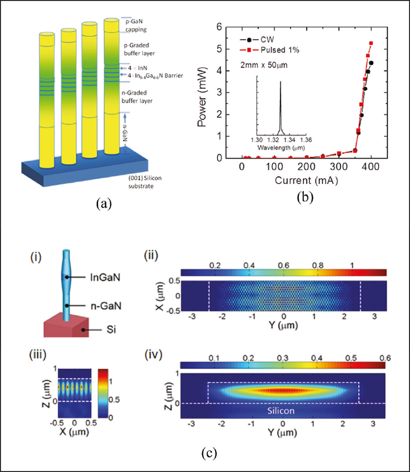
Figure 3. A 1.3 μm disk-in-nanowire array diode laser on (001) silicon. (a) a nanowire heterostructure with InN disks; (b) output light-current characteristics; (c) mode propagation and confinement calculated by the finite-difference timedomain technique.
To improve the performance of our edge-emitters, we adjusted the design, introducing a waveguide with a graded refractive index that has various compositions of InGaN. The device that resulted, which has multiple 6 nm-thick InN disks incorporated in the middle of the waveguide region, produces very promising output powers, good modal characteristics, extreme temperature stability (T0 ~220K) and a large differential gain, all at room temperature (see Figure 3 for details of the output light-current characteristics). With the emission peak at about 1.3 μm, our device is a promising candidate for silicon photonics.
Collaborators have simulated the performance of our lasers. Using the finite-difference time-domain method, Junseok Heo at Ajou University, South Korea, has studied the characteristics of the propagating mode (see Figure 3). Meanwhile, John Dallesasse and his group at the University of Illinois, Urbana-Champaign have calculated the strain distribution and bandstructure in the disks. Both studies have helped us to increase our understanding of the electronic and structural properties of the InN disks and the characteristics of the lasers made with them.
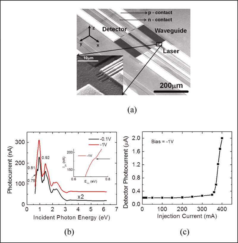
Figure 4. (a) Scanning electron microscopy image of a fabricated nanowire photonic integrated circuit on (001) silicon; (b) photocurrent response of integrated photodiode; response of photodiode to increasing injection current applied to the laser. The peaks and shoulders in the responsivity spectra result from interband transitions in the InN disks and other regions of the nanowire heterostructure.
To determine the usefulness of our lasers in communication-based applications, we have undertaken high-speed measurements on these devices. Using small-signal modulation measurements, we have found that our lasers can be modulated at frequencies of up to 3 GHz. This is by no means the limit of their capability: refinements to the design will increase this bandwidth.
Producing photodiodes
Another key component in even the simplest conceivable communication link is the photodetector. Success with our lasers has motivated us to investigate near-infrared guided wave photodiodes fabricated with the same nanowire array. This effort draws heavily on our previous work, because the only difference between the fabrication of our lasers and our photodiodes is that the reflective mirrors on the laser facets are replaced by anti-reflective dielectric coatings, made from SiO2.
Our photodiodes, which are typically 50 μm-wide and 1 mm-long, have been characterized under reverse bias. Dark currents are a few tens of nanoamperes. Meanwhile, responsivity is 0.1 A/W at 1.3 μm, according to measurements that use spectrally filtered light from a broadband source, directed through a monochromator and collected by a fibre that is focused on a facet of a photodiode (see Figure 4).
Following the fabrication of these devices, we have realized and tested an entire photonic integrated circuit consisting of a laser, photodiode and a waveguide. For the latter component, we have turned to an InN/InGaN/GaN heterostructure disk-in-nanowire arrays, identical to the one used for the fabrication of the 1.3 μm laser and photodiode (see Figure 3). Again, growth was by MBE, on a (001) silicon substrate.
III-Nitrides beyond the near-infrared
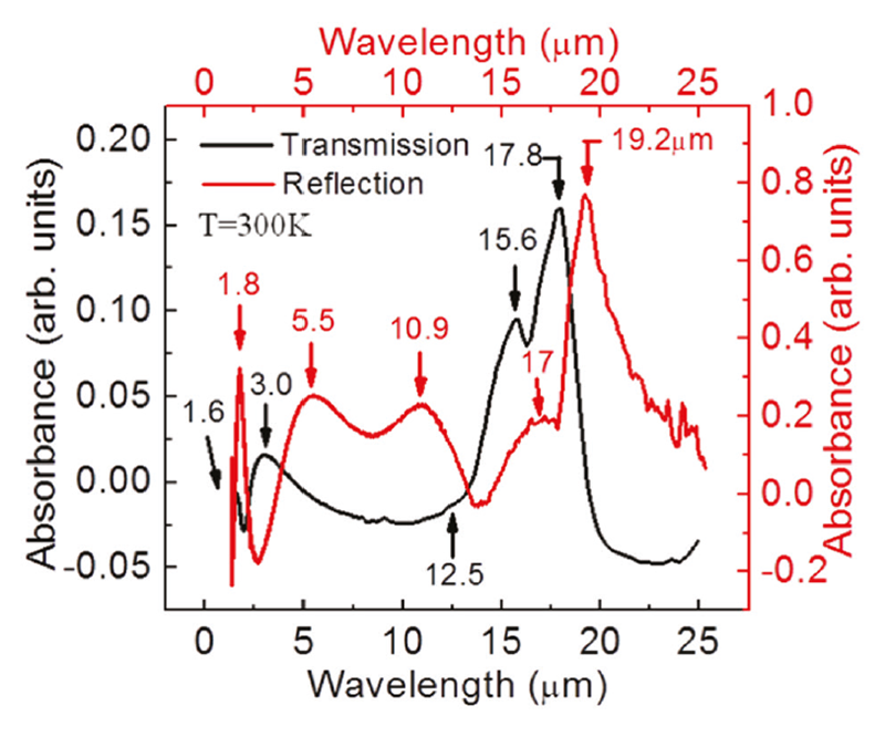
Significant research is being undertaken to explore applications of III-nitride materials beyond the near-infrared. The detection of light beyond 1.6 μm is possible by utilizing intersubband electronic transitions, rather than interband transitions. Intersubband transitions have been observed in In0.34Ga0.66N/GaN heterostructure nanowire arrays grown epitaxially on (001) silicon.
The polarization field in the InGaN disks is weaker than that in GaN equivalent quantum wells, due to strain relaxation in the nanowires during epitaxy. Consequently, the band bending in the active region is weaker, leading to a larger number of electron and hole bound states. Electronic intersubband transitions take place between these bound electron and hole states during absorption of infrared light in the 3-20 μm spectral range. Measurements of absorption peaks in an array of In0.34Ga0.66N/GaN disks-in-nanowires have been made by Alexander Soibel and Sarath Gunapala from the NASA-Jet Propulsion Laboratory (see Figure).
Infra-red absorption has applications in a wide range of fields, including chemical spectroscopy, and terrestrial and extra-terrestrial communication. These applications could be targeted by detectors based on nanowire-based technology that offer significant advantages over the traditional infrared detectors, which unite compound semiconductor based detector arrays and silicon readout integrated circuits with indium-bump bonding. This expensive technology is avoided, as nanowire array infrared detectors are epitaxially grown on silicon. And there is also the promise of room-temperature operation!
To fabricate the photonic integrated circuit, we used process steps that are identical to those employed for the two active devices. However, we used an extra dielectric deposition step to form a multi-layer Si3N4/SiO2 waveguide between the laser and the detector. Waveguide deposition parameters were optimized to minimize waveguide loss, measured in identical control waveguides. To improve the quality of the communication link, we deposited a ZnSe/MgF2 multi-layer distributed Bragg reflector (DBR) on the laser facet that is away from the waveguide, and added a SiO2 anti-reflective coating on the detector facet away from the waveguide.
Further improvements resulted from the introduction of a reflective coupling facet of the laser to the waveguide. To accomplish this, air/semiconductor (nanowire-parylene) DBR mirrors were defined by focused ion-beam etching. Just four periods of this DBR can provide sufficient reflectivity for successful laser operation and waveguide coupling.
To test the complete optical link (see scanning electron micrograph image in Figure 4), we gradually increased the bias to the laser and measured the photocurrent of the detector. As we had hoped, the photocurrent behaviour is identical to that of the light-current characteristics of the laser, confirming that light from the laser couples to the detector via the waveguide. The input power to the photodiode, for the maximum measured photocurrent of about 2 μA, is estimated to be 20 μW.
Our results demonstrate that an optical communication link can be formed on a (001) silicon substrate, the platform for all CMOS circuitry, from monolithic integration of an epitaxially grown 1.3 μm laser, photodetector and waveguide. The next steps in the development of this technology may include the introduction of a light modulator, as well as laser and detector biasing circuits based on silicon transistors. While the primary application for our technology is optical communication on silicon chips, it could also serve in future optoelectronic and biomedical applications.
The work was supported by the National Science Foundation.
Further reading
A. W. Fang et al. Opt. Express 14 9203 (2006)
T. Frost et al. Nano Lett. 14 4535 (2014)
S. Wirths et al. Nat. Photonics 9 88 (2015)
A. Hazari et al. Appl. Phys. Lett. 107 191107 (2015)
A. Hazari et al. Appl. Phys. Lett. 109 191102 (2016)
A. Hazari et al. IEEE J. Quantum Electron. 53 (2017)
A. Hazari et al. IEEE Photonics Technol. Lett. 29 1751 (2017)
L. Yan et al. J. Electron. Mater., 1 (2017)

An international team of researchers led by the University of Bristol have demonstrated that light can be used to implement a programmable, multi-functional quantum processor.
The team has developed a silicon chip that can be used as a scientific tool to perform a wide array of quantum information experiments, while at the same time showing the way to how fully functional quantum computers might be developed from mainstream chip-making processes.
Quantum computers are instead based on “qubits” that can be in a superposition of the 0 and 1 states. Multiple qubits can also be linked in a special way called quantum entanglement. These two quantum physical properties provide the power to quantum computers.
One challenge is to make quantum computer processors that can be re-programmed to perform different tasks in a similar way to today’s computers
The chip developed by the Bristol team can fully control two qubits of information within a single integrated chip. This means any task that can be achieved with two qubits, can be programmed and realised with the device.
“What we’ve demonstrated is a programmable machine that can do lots of different tasks,” said Dr Xiaogang Qiang, who now works in the National University of Defence Technology in China. “It’s a very primitive processor, because it only works on two qubits, which means there is still a long way before we can do useful computations with this technology. But what is exciting is that it the different properties of silicon photonics that can be used for making a quantum computer have been combined together in one device. This is just too complicated to physically implement with light using previous approaches.”
“We need to be looking at how to make quantum computers out of technology that is scalable, which includes technology that we know can be built incredibly precisely on a tremendous scale,” said Dr Jonathan Matthews, a member of the research team based at the Quantum Engineering Technology (QET) Labs at the University of Bristol. “We think silicon is a promising material to do this, partly because of all the investment that has already gone into developing silicon for the micro-electronics and photonics industries. And the types of devices developed in Bristol are showing just how well quantum devices can be engineered.
“A consequence of the growing sophistication and functionality of these devices is that they are becoming a research tool in their own right — we’ve used this device to implement several different quantum information experiments using nearly 100,000 different re-programmed settings,” he said.
Further information Paper:
'Large-scale silicon quantum photonics implementing arbitrary two-qubit processing' by X. Qiang, X. Zhou, J. Wang, C. Wilkes, T. Loke, S. O’Gara, L. Kling, G. Marshall, R. Santagati, T. Ralph, J. Wang, J. O’Brien, M. Thompson and J. Matthews in Nature Photonics

A new study by scientists from the University of Bristol brings us a significant step closer to unleashing the revolutionary potential of quantum computing by harnessing silicon fabrication technology to build complex on-chip quantum optical circuits.
Quantum computers offer an exciting new approach to solving problems that are currently intractable even on the most advanced classical supercomputers.
Building a quantum computer in the lab however has proven to be highly challenging.
Researchers at the University’s Quantum Engineering Technology Labs (QET Labs) are using single particles of light, photons, to construct optical circuits that process quantum-bits (qubits) of information.
Using the same materials and fabrication facilities originally developed by the electronics industry, QET Labs have demonstrated highly complex circuits on silicon chips that can precisely process small numbers of photonic qubits. Their findings have been published in the journal Optics Express.
Although circuits can be made almost arbitrarily large it has proven difficult to generate many perfect and identical photons at the same time for processing larger amounts of quantum information.
The research team, headed by Dr Gary Sinclair and Dr Imad Faruque, set out to investigate if several parallel sources on a single silicon chip could be made to generate perfect and identical single photons.
Dr Imad Faruque said: “We demonstrated for the first time that nearly perfect single-photons can be generated from two parallel sources on the same silicon chip.
“To demonstrate this, we took photons from each source and performed a “quantum interference” experiment: the ultimate test of photon quality.”
The results showed that using current techniques photons generated in multiple sources in parallel can be made up to 92 percent identical to each other, and that it should be possible to improve this even further by using the latest methods proposed.
Dr Gary Sinclair added: “Generating many identical single photons in parallel is essential if we are going to scale-up the proof-of-principle experiments currently performed in the lab into something large enough to become a practically useful computational tool.
“Our experiment has experimentally demonstrated that this is feasible for the first time. This demonstration marks a major step in quantum computing in silicon with photons and clears the way for a rapid increase in the scale of quantum computing demonstrations that are possible.
“Although our demonstration is an important step, many more hurdles remain. Our next aim is to use the latest advances in source design to demonstrate that we can generate photons that are much closer to 100 percent identical than the 92 percent demonstrated so far.”
Paper: ‘On-chip quantum interference with heralded photons from two independent micro-ring resonator sources in silicon photonics’ by I. Faruque, G. Sinclair, D. Bonneau, J. Rarity and M. Thompson in Optics Express.
Synopsys and SMART Photonics have announced that a new, production-ready process design kit (PDK) based on SMART Photonics’ Indium Phosphide (InP) process is now available in Synopsys’ OptSim Circuit tool to support InP-based photonic integrated circuit (PIC) design and simulation. Synopsys’ PIC Design Suite, which comprises OptSim Circuit and OptoDesigner tools, provides a seamless PIC design flow from idea to manufacturing from a single solutions provider. The addition of the SMART PDK to OptSim Circuit, combined with the PDK’s availability in OptoDesigner, enables users to use the PIC Design Suite to schematically capture and simulate InP-based PIC designs with the SMART PDK building blocks, and then synthesize and verify a SMART-foundry-compatible layout.
As PIC technologies advance, photonic design automation (PDA) software has become critical for improving PIC design productivity, driving time to market, and reducing costs. PDKs provide a crucial link between PDA circuit simulation and layout tools by supporting efficient design concept verification, signoff checks, and mask generation. The Synopsys PIC Design Suite, together with the RSoft photonic device modeling tools, give PIC designers and PDK developers a powerful infrastructure for creating and using custom PDKs, which is vital for generating foundry-specific intellectual property (IP), as well as augmenting existing PDKs with custom components, such as the SMART PDK.
“PhoeniX Software was the first commercial software partner with a proven track record for designing photonic circuits. The acquisition of PhoeniX and the OptoDesigner tool by Synopsys strengthens collaboration further and enables customers to move forward to use a single partner for the full simulation and design flow,” said Jeroen Duis, business developer of SMART Photonics. “We have been working closely with the Synopsys team to complete our PDK for use with the OptSim Circuit and OptoDesigner tools. This will help our mutual customers create more complex designs with a higher quality and shortened time to market.”
“This is another example of a world-class PIC foundry taking advantage of the new opportunities offered by rapid advances in photonic integration,” said Tom Walker, group director of R&D for Synopsys’ Photonic Solutions. “We are excited to be working with SMART Photonics and to be able to give our mutual customers the ability to design advanced custom photonic applications using the SMART Photonics InP semiconductor process.”
The U.S. Defense Advanced Research Projects Agency (DARPA) Microsystems Technology Office is asking industry to develop relatively simple portable PICs for high-performance position, navigation, and timing (PNT) devices as an alternative to GPS for when satellite navigation signals are not available.
A PIC or integrated optical circuit provides capabilities for information signals imposed on optical wavelengths, typically in the visible spectrum or near-infrared, 850–1650 nanometers.
The Atomic-Photonic Integration (A-PhI) program seeks to develop trapped-atom based, high-performance PNT devices, reducing the complexity of these atomic systems by using PICs. According to the DARPA document, the photonic integrated circuits will replace the optical assembly behind devices such as sensitive and accurate angle sensors and clocks, while still enabling the necessary trapping, cooling, manipulation and interrogation of atoms.
Advanced Micro Foundry, a spin-off from Singapore's renowned A*STAR Institute of Microelectronics, is a Singapore-based manufacturer of Silicon Photonics integrated circuits. Partnering with Lumerical, a leading developer of photonic simulation tools, AMF today announced the availability of a Compact Model Library (CML) for its Silicon Photonics process.
Integrating multiple photonic components on a single chip enables Silicon Photonics integrated circuit chips to achieve unprecedented performance, functionality, and economies of scale when compared to traditional photonics equivalents; rendering Silicon Photonics invaluable in multiple technologies and market domains. Smaller form factor and performance gain present Silicon Photonics with disruptive opportunities which were never possible for traditional optics, limited by material which could not be integrated and scaled like electronics.
AMF’s Silicon Photonics process is ideal for applications such as cloud computing, cloud security, hyper scale data centers, 5G communications, autonomous vehicles, robotics, telecommunications, AR and VR, and point-of-care diagnostic systems. Through a decade long intensive effort, AMF developed a comprehensive silicon photonic device library, which includes active and passive functional blocks. These blocks are now able to be simulated through the new CML using Lumerical’s INTERCONNECT Circuit Simulator.
The CML includes passive devices such as optical waveguide device, wavelength division multiplexer (WDM), micro resonator devices, and fiber-to-waveguide couplers as well as active devices such as thermally tunable devices, high-speed modulator, and large-bandwidth waveguide photodetector.
Photonic designers can leverage these pre-developed blocks to design and verify their photonics products more quickly and efficiently without crafting physical prototypes. These predictive capabilities enable photonics designers to validate designs prior to manufacturing, create new product concepts, and explore long-term innovative photonics research such as quantum computing.
“Combining our decade of silicon photonic leadership with Lumerical’s 15 years of photonic simulation leadership results in a capability that will increase our customers’ productivity and throughput. I’m looking forward to accelerating the amount of Silicon Photonic based commercial products as a result,” said Louis Lee, Business Operations Director of AMF.
James Pond, CTO of Lumerical said “Silicon Photonics is a key technology in enabling photonics to realize it’s potential by taking it from the research lab into the commercial world. This collaboration with AMF will help Silicon Photonics make its huge impact on technology advancement.”
AMF Silicon Photonics CML is available immediately from AMF. AMF CML Reader licenses are available immediately from Lumerical.
Optical network firm Infinera has completed its acquisition of Coriant, a privately held supplier of open network solutions. The acquisition positions Infinera as one of the world's largest vertically integrated optical network equipment providers, adding approximately 2,100 employees, over 1,600 patents and more than 600 customers.
In connection with the purchase, Infinera issued 20,975,384 shares of its common stock and will pay a cash consideration of approximately $230 million, of which approximately $154 million was paid upon closing.
“This is an exciting day for Infinera. The acquisition of Coriant is a major milestone, expanding the scope of our vertical integration strategy across a powerful suite of packet optical solutions for our customers,” said Tom Fallon, Infinera CEO. “The acquisition immediately strengthens our ability to serve a global customer base and accelerates delivery of the innovative solutions our customers demand.”
Initial feedback from existing Infinera and Coriant customers has been positive.
“Coriant already delivers strong technical value across our network, and we expect a stronger Infinera that will enhance and satisfy the transport needs of the customers,” said Cayetano Carbajo Martín, Telefónica CTO. “With the combined products and solutions from both companies, we look forward to more innovation from Infinera both for packet data and transmission.”
“GTT’s clients expect industry-leading, differentiated network infrastructure solutions to ensure their networks are reliable and secure,” said Paul Monteiro, SVP, operations and engineering at GTT. “We welcome Infinera’s acquisition of Coriant which enables Infinera to provide a broader range of high-performance network infrastructure capabilities.”
“The consolidation of both companies marks a significant milestone for the industry. As two industry pioneers, we believe strongly in their potential to deliver game-changing, innovative technology that will power the future of networks,” said Buddy Bayer, chief network officer at Windstream.
“We are excited to see Infinera’s acquisition of Coriant and anticipate that not only will we benefit from their combined innovation, but also their enhanced customer service as we invest in expanding our network footprint over the next five years,” said Conrad Mallon, chief technical architect at SSE Enterprise Telecoms. “It will be interesting to see how the orchestration and software strategy of the combined organisations develops and how they contribute to the world of SDN and NFV.”


Nanoscribe’s on-chip 3D micro-printing enables the creation of optical and MEMS components directly onto PCBs as well as electronic and optical device structures to support the development of photonic integrated circuits (PICs).
The growing demands of high-speed data communication, unmanned aerial vehicles and portable medical devices are but a few of the industries that can benefit from Nanoscribe’s new direct laser writing technology for additive manufacturing. The company is presently utilizing its technologies to produce photonic and electronic device structures to support wide-ranging applications in research and industry. Additive manufacturing at the nano scale enables designers and manufacturers to avoid some of the traditional processing steps employed to create electronic/ photonic circuits. Nanoscribe’s highest resolution 3D printers can print and integrate microscopic components directly on integrated circuits such as micro-lenses for photonic circuit applications and deformable structures for MEMS actuators.
Nanoscribe GmbH (Eggenstein-Leopoldshafen, Germany) designs and builds 3D printers for nano-, micro- and meso-scale applications as well as photoresists and process solutions. The company began as a spin-off of the Karlsruhe Institute of Technology (KIT, Germany) and now serves global research and industrial markets. Nanoscribe has received a number of awards and recognitions for its technologies including a 2014 Prism Award and the 2015 WTN Award. Nanoscribe was also a finalist in the 2015 Deutscher Gründerpreis competition (German Founders’ Award).
Nanoscribe’s groundbreaking technique enables the smallest objects with complex geometry and feature sizes (from hundreds of nanometers up to several millimeters) to be printed directly on wide-ranging materials common to electronic and photonic manufacturing. They are produced in a single printing step and on a scale which was previously inaccessible to 3D printing.
Nanoscribe’s Photonic Professional GT system uses two-photon polymerization to print nano scale device features. In this printing process a laser exposes a photosensitive resin by means of a high-numerical aperture objective along a controlled trajectory, layer-by-layer, that follows the pre-drawn CAD design. The material being printed solidifies only in the laser focus spot, which allows for a wide range of 3D structural types with even submicron features. The precision optics and advanced software tools of the Nanoscribe system enables the fabrication of 3D polymer structures with extreme precision, making the strengths of additive manufacturing available to micro- and nanofabrication including full 3D design freedom and a simple workflow from CAD model to final part. This process supports rapid design iteration cycles that save time and costs during product development. Additionally, the wide choice of print surfaces now also includes pre-patterned chips, making it possible to add 3D miniaturized functional parts to highly integrated circuits.

Image 1

Image 2
Nanoscribe printed a series of hemispherical micro-lenses (Image 1) onto photonic chips for the first time to demonstrate the capabilities of its unique hardware and software technologies. The micro-lenses were fabricated on top of grating couplers previously patterned on a photonic chip (Image 2). Using this technique, an array of micro-lenses can couple light into the circuit. The micro-optics were created in one printing step and without the need to align and mount the finished micro-optics mechanically into the pre-structured microchip. This process of direct fabrication of components onto existing circuits reduces packaging costs in equipment and saves time in calibration. Moreover, it avoids pick and place as well as curing-based fixing procedures. Taking advantage of the laser accuracy, 3D micro-printing also offers submicron precision and optical quality surfaces that meet the requirements for high performance micro-optics. Altogether, these benefits make this manufacturing technique a valuable method for in situ fabrication of micro-optics onto PICs for higher data transfer in telecommunication.
3D printed micromechanical components on MEMS actuators
3D micro-printing also benefits the development of new microelectromechanical systems (MEMS) actuator structures utilized in medical imaging and tissue regeneration amongst other applications. Professor Alice White at Boston University utilized Nanoscribe’s latest micro-printing techniques to fabricate deformable, bowtie-like structures directly on MEMS actuators (Image 3). These structures can stretch and bend and otherwise deform in a characteristic manner due to their design and 3D geometry. Deformation occurs through the application of low-voltage current.
“We have shown that coupling 3D micro printing with MEMS actuators is a powerful way to produce 3D micromechanical systems tailored to specific needs. Nanoscribe 3D printers allow us rapid prototyping of submicron-resolution structures that would otherwise be impossible to fabricate via single-photon stereo-lithography or the deposition and etching processes commonly used in semiconductor foundries,” said Professor White. The university is exploring methods to utilize the dynamic actuation of 3D printed microstructures for deformable optics and micro-miniature ‘scaffolding’ for tissue engineering experiments. This foundational work hopes to find better methods for restoring tissue that has been lost or damaged.

Image 3 – Boston University, under the direction of Professor Alice White, has successfully utilized Nanoscribe’s 3D micro-printing processes to create deformable optical and MEMS components for ongoing experiments into tissue engineering.

Image 4 -- CMOS-Chip: Lens stacks with different focal lengths printed onto a CMOS sensor for "foveated imaging". (Universität Stuttgart/PI 4)
Researchers from the University of Stuttgart used a Nanoscribe Photonic Professional GT system to print micro-objective lenses with different focal lengths onto a high-resolution CMOS chip. All images created by the lenses on the chip are simultaneously read out electronically and processed into an image with a significantly improved resolution in the center. This so-called ‘foveated imaging’ is very attractive for the production of cameras with sensors that mirror the extra-wide field of vision of an eagle's eye, e.g., for applications in automotive or smartphone industries as well as in the medical field.

Image 5 -- Semisphere micro-lenses with steep slopes and smooth surfaces are directly fabricated with a Photonic Professional GT.
This array of hemispheres (or semispheres) demonstrates the high shape accuracy and optically smooth surfaces achievable by using two-photon-polymerization. The printed hemispherical micro lenses have a shape accuracy better than 1 μm and a surface roughness better than 10 nm Ra. The array with a size of 1 square centimeter in total and hemispheres with a height of 150 μm was written into a solid negative tone resist. Due to the optimized combination of hardware and software components one can achieve a high and consistent precision on the whole area of the writing field.

Image 6 – Diffractive optical elements (DOE) can also be printed utilizing the Nanoscribe system.
Using a Nanoscribe system, the fabrication of diffractive optical elements (DOE) which typically have significantly smaller feature sizes than refractive optics, is possible as well. DOEs can be designed for functionalities that are hardly accessible with refractive optics, such as the generation of almost arbitrary light distributions in the far-field. By means of a Photonic Professional GT, functional multilayered diffractive optical elements can be directly patterned onto glass substrates within 10 to 20 hours enabling rapid prototyping and design iterations.
Nickel Shim
The challenge of fast and low-cost production of micro-optical elements can be solved by fabricating a nickel shim from the printed polymer structures by electroforming, allowing standard replication techniques such as injection molding or hot embossing to be used for subsequent mass replication; nanoimprinting is another viable replication route.
Summary
Nanoscribe’s 3D printer Photonic Professional GT allows producing almost arbitrary micro-shapes with optically smooth surfaces in an additive and tool-free way. This effectively circumvents limitations imposed by mechanical tools, and geometrical or process design-constraints often encountered with techniques such as subtractive machining, (greyscale) lithography, photoresist reflow and wet-etching. In this way, steep slopes for high numerical aperture micro-lenses, arrays with high filling factors and varying curvatures, as well as more complex 3D shapes can be achieved. Mass replication is possible by using metal replicas of these shapes.
Image 7 – Nickel-shim (right), fabricated from a 3D printed polymer master (left).
Earlier this year, Canada-based III-V photonics consultancy, Intengent, joined forces with US compound semiconductor wafer fabrication foundry, Global Communication Semiconductors, and photonics IC design house, VLC Photonics, from Spain, to take InP photonic IC development to commercial production.
Together the partners will offer fabless development for the production of customised InP PICs, and Intengent chief executive, Valery Tolstikhin, is certain that the new team has what it takes to deliver a generic InP PIC platform for industrial-grade wafer fabrication.
As he points out, GCS is one of the world's biggest III-V commercial foundries, churning out InP, as well as GaAs and GaN wafers, for RF electronics and optoelectronics markets in large volumes.
Meanwhile, Tolstikhin himself, has pioneered a re-growth-free photonic integration platform - Taper Assisted Vertical Integration - based on the GCS's well established optoelectronics process, for designing and developing InP PICs.
Factor in the VLC Photonics' design library and process design kit expertise, which is already applied to other commercial PIC platforms and can slash PIC design effort and risk, and Tolstikhin's confidence becomes understandable.

"Typically, people in the industry have an idea of the application they want to serve but often, don't know what device they want," highlights Tolstikhin. "So we can conceptualize the PIC that matches that application and develop it through regular design-manufacturing-verification cycles - that's what we do as a Consortium."
"Intengent provides the integration platform and underlying epitaxy design, VLC brings a wealth of experience in PIC design and characterisation, and GCS is probably the biggest commercial foundry in the III-V photonics domain," he adds. "I have seen optics increase from 5% of GCS's overall volume to more than 50%; this is a huge change and this [one-stop shop for InP PICs] is something I have wanted to be part of for a long time."
Early days
In the last two decades, Tolstikhin has launched several PIC-based businesses, pioneering various photonic integration platforms based on different versions of vertical integration.
He first became involved with PICs in 2000, when he joined MetroPhotonics, a spin-off from the National Research Council of Canada, set up to commercialise wavelength-division multiplexing technology for InP. Here, he led PIC design until the company folded in 2005, and during this time developed and patented a robust, regrowth-free active-photonic device integration technique called 'Single-Mode Vertical Integration'.
Having developed a number of InP-based WDM components at MetroPhotonics, he went onto launch OneChip Photonics, with a view to developing cost-efficient InP PICs using his regrowth-free PIC technology.
The OneChip business model was based on fabless manufacturing, which Tolstikhin has always touted as being appropriate for low volume markets. And during his leadership at OneChip, he honed his vertical integration process, pioneering 'Multi-Guide Vertical Integration'.

Here, by vertically stacking the necessary materials for, say, lasers and detectors, the technology allowed the company to monolithically integrate active, as well as passive, devices onto the same substrate in a single epitaxial growth step.
As the chief executive highlights: "I individually designed every single epitaxial structure for every PIC product developed or tried by OneChip, which was an absolutely crucial step in regrowth-free PIC production."
OneChip went onto develop PIC-based optical interconnects for 100G datacentre market applications, partnered with GCS and IQE on wafer processing and epitaxial growth but closed in 2014, by which time Tolstikhin had co-founded ArtIC Photonics, a fabless developer of InP-based PICs for telecoms and datacoms markets.
ArtIC remains today, designing PIC chips for optical component products, but in 2015 Tolstikhin founded Intengent to design and develop InP PICs, this time based on Taper Assisted Vertical Integration (TAVI).
Building blocks
The TAVI library comprises many building blocks, from lasers to amplifiers to detectors on the active device side and splitters/combiners, filters, and various elements of waveguide circuitry, on the passive device side. What is common to all of them is a lateral taper assisted adiabatic transition between vertically stacked and functionally different guiding layers.
Perhaps, the most generic building block, which showcases the TAVI platform from this prospective, is the spot-size converter that permits the transition of guided light from a PIC waveguide to an optical fibre. This is defined by building lateral tapers in a specially designed multilayer epitaxial structure. Indeed, as Tolstikhin points out: "Intengent has now been working with a commercial foundry on the epitaxy growth of specialised wafer designs that comprise up to 90 layers."
"It is so important to allow the optical signal to move from one vertical layer to another.... and lateral tapering allows you to vertically connect all of your waveguides," he adds. "This method is very flexible, it is a big deal and we are seeing big gains in reliability."
Right now, Intengent is predominantly working on four inch wafer sizes with GCS, but intends to transition to six inch wafers as soon as possible.
"I would love to work with six inch, even eight inch wafer sizes but these are not readily available right now," says Tolstikhin. "In terms of cost, size of wafers really does matter here as the number of devices you can harvest is so different from wafer to wafer; this is not like laser development, these really are big chips."
"I cannot name the date, but six inch wafer fabrication is coming," he adds.
Crucially, so is demand. According to Tolstikhin, he is thinking of expanding the company to cope with growing demand for InP-based PICs from various segments of the market, from tele- and Datacom to microwave photonics and quantum inscription.
And at the moment, the chief executive is also seeing interest from silicon photonics businesses demanding III-V integration. "[Designs] now need sophisticated light sources that cannot be provided by off-the-shelf by bulk assembly," he says. "This is one avenue that wasn't really evident a few years ago."
With demand rising, Tolstikhin is now looking forward to seeing what he describes as 'real commercial infrastructure' for the fabless development of III-V photonics. He hopes such infrastructure will be in place within the next five years, and importantly, he expects this to be able to provide a full level of customisation, within a reasonable budget.
"Following the development of silicon photonics, many in our industry now understand the need for fabless development and the pointlessness of building an entire infrastructure for just one device," he asserts. "We are trying to capitalise on this and provide the services that those people want."

In the next few years, we are going to see the incorporation of photonic technologies in many new products that will provide consumers with a new range of functionalities in such fields as telecommunications, healthcare and the environment. Electronic circuits shook the industry many years ago, and it’s now time for photonic integrated circuits (PICs) to replace them to produce a new generation of products. All the infrastructure necessary to build this new industry is now being assembled and the main actors are being appointed. In this article, we will look at the characteristics that position PICs as one of the key enabling technologies for the next industrial revolution. We will also review the different steps in the development of photonic products, and the capabilities that are available right now as well as the companies and organizations working in this new field.
by Ana Gonzalez, EPIC R&D Manager
Characteristics of PICs
Matter can interact with light, emitting or absorbing energy causing common optical phenomena such as rainbows, our reflexion in a mirror and the colour of everyday objects. Less well known by technical non-specialists is that light can also be confined in a material of very reduced dimensions, from micrometres to nanometres - so-called ‘waveguides.’ In a waveguide, different refractive index materials are employed, light is shaped, and it can propagate in its single-mode or multimode state. The technology that uses waveguides to perform optical functions (as just described) is called photonic integrated circuits (PICs).
Photonic integrated circuit technologies are impacting in different mass-markets such as telecommunications, sensors and healthcare. The introduction of PICs to improve existing products presents several advantages, such as miniaturization, cost reduction, and lower energy consumption. In telecommunications, the growing demand for more bandwidth density and data transfer is driving the incorporation of PICs in telecom and datacom transmitters and receivers. These new systems will reduce the overall power consumption of a data centre and bring down costs and its CO2 footprint. Necessarily, the new optical interconnect interfaces will be based on photonic integration and CMOS compatible photonics, the only mass manufacturing technology capable of meeting all these requirements. Despite the fact that the main application for PICs are telecommunications, they are also being increasingly used in the (bio)sensing field, opening up new opportunities for the development of diagnostic tools for personalized medicine and point-of-care (POC) devices. Currently, the clinical detection of biomarkers in disease detection is often performed using ELISA assays, which are time-consuming, involve a number of complex steps, and must be carried out at specialized laboratories by skilled personnel. However, PIC-based biosensors can enable direct detection at any place and anytime, without the requirement of additional steps or a laboratory. While the efficacy of PIC and semiconductor-based biomedical analysis is still evolving, the prospects, convenience and potential to reduce costs are driving growth opportunities.

The possibility of embedding some photonic functionalities into an integrated optical chip can simplify a system and dramatically decrease its cost. As an example, Optical Coherence Tomography (OCT), an imaging technique that captures micrometer-resolution, three-dimensional images from within optical scattering media such as biological tissue, can be miniaturized by using PICs, as can be seen in Figure 1. This means that what are now various bulky and expensive optical components can be replaced by PICs, avoiding the assembly of the components, allowing a reduction in price and size.
The next section will explore the manufacturing value chain that will allow the production of PIC-based products in Europe, highlighting the available technologies and main actors who will lead the introduction of PICs into mass-markets.
Design of PICs
Light propagation in an optical waveguide is described by Maxwell's equations, which means that the waveguide can be optimized to provide a specific behaviour and characteristic of the propagated light. There is a strong market in Europe in the development of software and process design kits (PDK,) containing component libraries that include the mask layout and accurate models of the building blocks in the foundry platform and the design and validation of photonic integrated circuits. Companies offering these services include VPI Photonics, CST, Phoenix Software, and Luceda.
PIC Foundries
The substrates most commonly used for the fabrication of PICs are silica-on-silicon (SiO2 / Si), silicon nitride (SiN), and III-V semiconductor compounds, such as indium phosphide (InP).
SiN/SOI (Silicon-on-insulator) is one of the most prominent platforms for PICS due to high refractive index contrasts (very high for SOI and moderately high for SiN) and compatibility with CMOS (complementary metal-oxide semiconductor) electronics. SOI-based PICs have low absorption losses in the wavelength range from 1.1 µm to about 3.7 µm. For applications requiring shorter wavelengths, SiN is a good candidate as it is transparent throughout most of the visible range. Foundries for SOI technologies are IMEC, LETI, IHP and VTT and for SiN technology they are LioniX (TripleX) and IMEC.
InP offers the possibility of an important level of monolithic integration. It is used to produce efficient lasers, sensitive photo detectors and modulators in the wavelength window typically used for telecommunications. Due to its high refraction index, devices are very small, but the optical loss is also relatively high, so InP is not typically used for passive functions. The foundry service providers for this technology include HHI Tx-Rx and SMARTPhotonics.
Such devices are fabricated in costly clean-rooms that provide access to fabless customers. Multi-project wafer (MPW) runs provide a solution for companies in the start-up phase to prototype and validate their designs. This solution consists of combining multiple designs from various teams and integrating them on one wafer leading to a significant reduction in research and development costs, allowing the sharing of mask and wafer resources to produce designs in low quantities. The PICs fabricated in such MPW runs are called ASPICs (Application Specific PICs).
Packaging and Assembly of PICs
Miniaturization is one of the advantages of PICs based products. However, in such small devices, the connection with the outside world is a challenge and requires a diverse range of technical competencies to make the optical, electrical, thermal and mechanical connections. The critical issues in a PIC based product are the micron-level alignment of optical components, temperature control and a high degree of vertical and horizontal electrical integration. Ensuring that these devices are fully functional when fabricated and assembled requires the adoption of packaging design rules (PDR) at the PIC design stage.
Optical packaging
Electronic Packaging
Electrical-routing structures are sometimes required for photonic packages: they are called PCBs (Printed Circuit Boards, see Figure 2). The gap between the PIC and the transmission lines can be bridged by a ceramic interposer. The electrical connection between the interposer and the bond-pads on the PIC are made using gold (Au) wire-bonds. “Glop top” encapsulation of the wire-bonds with silicon or epoxy can offer further protection. If a very high number of electrical connections to the PIC are needed, then vertical integration of an electronic integrated circuit (EIC) can also be required. The vertical integration of an EIC on a PIC can be made using either solder-ball-bump or copper-pillar-bump interconnects, which provide an electrical, mechanical, and thermal interface between the two chips
Figure 2. Flexible Transmitter, the PIC is integrated with a PCB. Courtesy of Cordon Electronics Italia.

Thermal Packaging
Photonic elements, such as sensors, exhibit strong temperature dependence. The thermal stabilization of the PIC in a photonic device with a thermoelectric cooler is essential for prototypes that need to be tested in the field. Finite-element simulations in COMSOL can be used to test and optimize new stack designs, which are then experimentally validated using the dynamic temperature measurements from thermal microscopy.
Conclusions
The high cost and low-speed of photonic packaging is probably the most significant bottleneck in developing competitive photonic devices. The need to create standardized design rules and standards for photonic packaging is gaining support as having these could reduce the price of PIC-based products. The challenge of assembling and packaging PICs is now shifting to automating the processes (see Figure 3), the development of package standards and mass-scale testing. These are the goals of PIXAPP (a pilot line for PIC packaging and assembly), a European initiative that joins the leaders in packaging technologies. PIXAPP bridges the ‘valley of death’ often associated with moving from prototyping to low-volume fabrication, by giving companies an easy-access route to transferring R&D results to the market.

Figure 3. Automatization of the assembly process of PICs. Courtesy of ficonTEC.
For further info: https://pixapp.eu/
[1] Lee Carroll et al. Photonic Packaging: Transforming Silicon Photonic Integrated Circuits into Photonic Devices. Appl. Sci. 2016, 6, 426
Dr. Ana González is R&D Manager at EPIC (European Photonics Industry Consortium). Her expertise relies on the development of systems based on integrated photonic circuits, packaging and assembly, and the investigation of applications such as chemical/biological sensing and Datacom. In addition, she has been involved in technology transfer and business development processes. She received her Bachelor’s degree in Chemistry from the University Autonomous of Barcelona (UAB) and her PhD degree from the Catalan Institute of Nanoscience and Nanotechnology (ICN2).

EPIC Meeting on Automation Tools for Packaging and Testing took place on 22-23 May in Karlsruhe, Germany, at the headquarters of PI (Physik Instrumente). The purpose of the meeting was to bring together equipment manufacturers and companies investing or interested in the further automation of their high precision manufacturing and testing lines, to discuss the production of optoelectronic components and modules (silicon photonics, PICs, AOC, VCSEL, laser diode, WLP, 2.5D/3D IC, TSV, TCB, fan-out/EWLP,…)
and to identify bottlenecks in process automation for any industry (HPLD manufacturing, fibre optics and opto-electronics, medical technology, security and military applications, R&D, telecommunications, and others) and volume demand. There were 15 presentations and 40 participants from 12 countries, with the presence of EPIC members like Jenoptik, ficonTEC, VTT, imec, Yelo, IRSweep, Nanosbribe, CESEM, Xeryon, TNO, QPO lenses, Aifotec…
EPIC Meeting on Singlemode vs Multimode Communication took place on 11-12 June at CommScope, in Kessel-Lo, Belgium. The meeting focused on the key important aspects to consider when choosing a single mode or multimode approach for a communication link. The large number of parameters to consider, as well as some myths and truths were discussed by suppliers, users and industry leaders.

The invited keynote speaker was Mark Lutkowitz, Principal at fibeReality. There were 18 presentations and 40 participants from 12 countries. During the meeting, there were many opportunities for networking, and the participants had the chance to visit CommScope facilities.

EPIC World Photonics Technology Summit took place last 30-31 August is Brussels. The purpose of this unique meeting was to bring experts and leaders from industrial companies around the world to discuss photonics technology developments and challenges.
The event was at CTO/CEO level, 1 representative per company, with an audience of 110 participants from 22 countries. The presentations were short (15 minutes) followed by 5 minutes of discussion moderated by Dr. Jose Pozo, EPIC’s Director of Technology, who engaged the audience to explore synergy and business opportunities.
The event was very much networking oriented with 11 such opportunities. EPIC meetings are held in a relaxed yet professional environment, with the purpose to get to know each other, get to know participating companies, the solutions, and especially the challenges.
As a tradition in the EPIC meetings the participants took their running shoes for a morning run before starting the second day of the meeting.
Upcoming PIC related EPIC events:
EPIC events are renowned for excellent networking opportunities for creating new connections and strengthening existing partnership connections. When EPIC members network and connect this means building trust within photonics industry leaders and experts.
13 November EPIC Tech Watch at MEDICA 2018, Dusseldorf, Germany
15-16 November EPIC Meeting on Environmental Monitoring at Avantes, Apeldoorn, The Netherlands
EPIC also hosted a VIP party at the ECOC Conference and Exhibition in Rome, Italy on 24 September.
Find out about upcoming EPIC events on www.epic-assoc.com/epic-events
Photonics influencers discuss the difficulties Europe faces in setting up manufacturing facilities, bringing products to market and finding talent.
Panel Members: Yossef Ben Ezra, Dean Holon Institute of Technology, Israel; Stephen Doherty, Program Manager, Viasat Antenna Systems, Lausanne, Switzerland; Annette Grot, Pacific Biosciences, Menlo Park, California, USA; Rick van de Zedde, Wageningen University, Netherlands; and Steve Walsh, Distinguished Professor, University of New Mexico, USA.
What about the difficulties of manufacturing in Europe?
The development of photonic integrated circuit (PIC) based products is gaining increasing interest in many different markets such as 5G, transceivers for datacom, LIDAR and (bio)chemical sensors. The PIC market based on silicon was valued at USD $626.8 million in 2017 and will reach USD $1,988.2 million by 2023 – a CAGR of 20.8 percent—according to researchers at Yole Développement, 2018. At the same time, InP PIC technologies already have 30 percent penetration by value for transceiver markets. The goal of the EU-funded pilot lines in photonics under the H2020 program is to keep European companies competitive by providing low-barrier access to new production services and by accelerating the time to market. However, the competition from other regions of the world is fierce. A round table during the World Technology Mapping Forum in Enschede (Netherlands) in June tried to unveil some of the strategy to keep Europe at the top of the game for the manufacturing of photonic integrated circuits.
1. Lack of government subsidies
One concern was the general impression that China values capabilities and competences more than Europe. The reason for a company to be transferred to China could not be based on that they have a better supply chain, or they could do anything faster. Nevertheless, the Chinese government could provide a two-billion-dollar facility for free. This is enormously attractive as 95 percent of the costs of components like semiconductors could be tied to infrastructure costs and only 3-5 percent comes out in labour costs.
2. Ecosystem and the supply of subcomponents
Another problem for Europe is the lack of a mature supply chain, i.e. a concentration of companies able to supply subcomponents like PCBs, resistors and capacitors. In the US, these companies are spread out, but in Asia you have 50 of 100 of them all in the same city making it more attractive from a business standpoint. In this context, Europe might do well to emulate China by providing incentives to help develop a European supply chain. For example, starting in the 80s and 90s China had imposed conditions on US companies such as requiring that if a company moved production to China, they had to buy 50 percent of materials needed for manufacturing from the Chinese supply chain.
3. Lack of imagination
For some people in the US, there is a lack of imagination and vision in risk-taking on the part of the European business community. While European technology and science is excellent, there are relatively few business initiatives emerging from Europe that can be capitalized upon.
Kaiam: A European success story
Despite these challenges, photonics companies are manufacturing in Europe. A case in point is Kaiam which originally manufactured in China but has since moved back to Scotland to produce 100G-CWDM4+ transceivers. Apart from still having to send sub assemblies to China for testing, their manufacturing is now 100 percent in Europe.
Process control and wafer level testing
After 30 years, so little progress had been made in developing control processes in photonics similar to those in silicon. Without adequate control processes, it will be impossible to develop a truly integrated approach and a roadmap for future growth. This control of processes can only be achieved through inspections at wafer level after every process. This will enable acceleration of new IC designs and process verification by assessing the reliability characteristics and improving repeatability. It also makes sound business sense as testing at wafer level is much cheaper than testing modules independently.
Standardization
In microelectronics, measuring different physical and process parameters is relatively simple, but with silicon photonics it's more problematic because of the variety of applications: some have a passive silicon device while others may have 3-5 active components integrated on the silicon. So, a prerequisite for testing and monitoring in silicon photonics is to define each of the parameters to be tested.
The diverse range of applications is a particular challenge for establishing packaging standards. Around 80 percent of component costs lie in packaging and testing and if the photonics industry cannot come up with a standard package, it will be impossible to make components cheaply enough. What has proved particularly difficult is optical fibre connections from both ends of the chips. These connections need fine accuracy, but standardisation has proved difficult due to variabilities in chip size. Another of the problems in standards is allocating the costs and responsibilities, e.g. the systems integrator, the component integrator or the packager—compounding this fact is that costs must be shared out equally.
There is also a need to develop tools capable of providing repeatable and reliable measurements. As Annette Grot of Pacific Biosciences succinctly put it, "if you can't measure it, you can't control it". It would therefore be useful for the photonics industry to work more closely with tool manufacturers to establish standards to grow the industry.
Future opportunities and challenges
A summary of recent forecasts (2013-2017) indicates a 10-20 percent sector growth in markets where InP PIC may be expected to have impact. InP PIC technologies already have 30 percent penetration by value for transceiver markets. Production will be significantly more profitable as engineering support is distributed across higher volumes, enabling lower chip prices for users and lower production costs for suppliers. However, the value of the chip is a fraction of the module cost, typically 10% of module cost for the more established product lines in telecommunications, residential broadband, consumer products and even fibre optic sensors. Then, the packaging and assembly of PICs are bottlenecks in the manufacturing of PICs-based products. Here, the challenge is to keep European companies competitive by providing low-barrier access to new production services and by accelerating the time to market. This is the goal of pilot lines in photonics: MIRPHAB (for prototyping miniaturized chemical sensors based on mid-IR technology), PIXAPP (for packaging and assembly of PICs) and PIX4Life (Si3N4 PICs for healthcare applications). Pilot line initiatives focus on the reduction of the costs for the production of PICs by the development of standards and the automatization of the process aiming to strengthens Europe’s position in the manufacture of photonics devices. These markets will be enabled by new products out of the traditional datacom.
Quantum technologies would be an example of increasing investor activity, particularly in quantum cryptography as security is seen as key for the future. Biophotonics is also gaining attention, but there are still gaps in the supply chain. For example, for optical coherence tomography, the biggest challenge in getting photonic integrated circuits into hospitals is the lack of system integrator companies to act as intermediaries between hospitals and technology producers. A possible solution will involve joining R&D programs between clinicians and photonics companies. This would help to develop the products required by clinicians and make clinicians more aware of how photonics can help to improve patient care. Also, the technology currently available is not able to support some areas of pharmaceutical research such as the continuous quality control required for many drugs. There is a need for system integrators to incorporate PICs in their systems to bridge the gap.
Finding Talent
A major hurdle in the development of European photonics industry is the scarcity of talent. The problem is not only contracting and holding on to personnel with the required training, experience and competencies, it's also the fact that many photonics technologies need interdisciplinary teams to develop.
The experience of Pacific Biosciences in this respect was outlined during the panel discussion. The company started out at Cornell University in the middle of New York, but venture capitalists would only put up funding for growth if the company moved to Silicon Valley. This condition was based on the recognition by the venture capitalists that health care technologies can only develop using a variety of skills via an interdisciplinary approach. The result was that the company moved to Silicon Valley, hired a CEO who was a proponent of optical communication and computation paired with efforts to bring in personnel from a variety of backgrounds including telecommunications, IT and biosciences.
This underlies the importance of location. Talent is part of the ecosystem and just as concentrations of subcomponent manufacturers are important for supply chains; photonics companies that set up or move near to concentrations of talent will be better able to recruit and keep talent, create multidisciplinary teams and obtain funding.

Dr. Ana González is R&D Manager at EPIC (European Photonics Industry Consortium). Her expertise relies on the development of systems based on integrated photonic circuits, packaging and assembly, and the investigation of applications such as chemical/biological sensing and Datacom. In addition, she has been involved in technology transfer and business development processes. She received her Bachelor’s degree in Chemistry from the University Autonomous of Barcelona (UAB) and her PhD degree from the Catalan Institute of Nanoscience and Nanotechnology (ICN2).

Fast Multichannel Photonics Alignment (FMPA) represents a clear break from the past in ways that are highly relevant to the advent of silicon photonics (SiP). Scott Jordan, Sr. Director, NanoAutomation Technologies, Head of Photonics, PI (Physik Instrumente) L.P.explains
The first computer link using optical fibers was commissioned four decades ago to safeguard communications from electromagnetic interference at the Cheyenne Mountain strategic command center in Colorado Springs, Colorado. Since then we have seen broad adoption of photonic communications technologies in an unfolding pattern of consistently diminishing physical scale. Milestone advancements include their implementation…
a) as a replacement for costly and ‘laggy’ satellite links for transoceanic telecommunications;
b) as the backbone of transcontinental communications, first for voice land-lines and later for data communications;
c) as the foundation for regional and metropolitan communications infrastructure;
d) as a delivery mechanism for bandwidth to businesses and consumers, including to the home;
e) most recently, as a scalable and high-capacity mechanism for data links across and between data centers, then from rack-to-rack, then box-to-box and card-to-card, and soon from chip-to-chip. IBM has even spoken of a ‘gaudily’ multi-core future chip architecture with hundreds of cores all interlinked by an on-chip optical mesh.
This unrelenting drumbeat of advancement and the monotonic diminishment of scale were interrupted by the industry die-back in the early 2000s as overcapacity and an economically unsustainable glut of under-differentiated ventures combined to harrow the field. In hindsight, this bow to “photonomics” seemed inevitable as supply and demand found themselves catastrophically imbalanced. It meant for a quiet decade-and-a-half, but only from a commercial sense. Technologically, the steady down-drop in scale continued in research and industrial laboratories. The goal – elimination of copper as the default interconnect. The promise – bounties of capacity, throughput, parallelism, scalability and energy savings.
About five years ago, the semiconductor industry began driving photonics, the fruit of advancements in technologies that facilitated the leveraging of light within silicon structures. This merger of technologies reflected a merger of destinies. In the photonics doldrums of 2002, no one was talking about streaming media, Big Data, or the Internet of Things. There were no iPhones with their media-enabled browsers in anyone’s pocket, no GPS apps with always-updated maps, traffic and routing data, no smart factory equipment driving artificially-intelligent prognostics to maximize uptime. Video-calls were a fanciful attraction for dazzled suburbanites to gaze upon in AT&T’s Tomorrowland attraction. Music was bought on CDs at record stores, and movies were rented on tape cassettes at Blockbuster. As new wonders swept these aside and became everyday fixtures of civilized life over the past decade (one decade!), as waves of creative destruction washed away entire industries, bandwidth demand proceeded methodically along its exponentiating path. Eventually, the photonics industry came back – because it had to.
Alignment Emerges
There was a time when testing and packaging a photonic device just meant attaching a single optical fiber to a single emitter or detector. Even in the early days of single-mode fiber optics in the late ‘80s and early ‘90s, this posed significant challenges. Such couplings are typified by a Gaussian cross-section (though departures from the idealized mathematical profile are common). For transverse misalignments of two parallel circular optical waveguides of waist radii w1 and w2 this equates to a transmission T that diminishes with lateral misalignment as d Equation 1.

Equation 1 – A classical Gaussian coupling. (Image PI)
As can be readily calculated, in the common case where w1 = w2 a misalignment of half a waist radius results in a diminishment of coupling throughput by 1dB; misalignment of a full radius diminishes coupling by a whopping 4dB. The steepening slope of the Gaussian means that drift and other misalignment processes start bad and get worse. It also means that recovering from an initial misalignment is a tweaky process since orders of magnitude of coupling change can result from only a small change in mutual alignment. Multi-mode fibers and devices are not necessarily easier to align, since determining the location of their globally optimum orientation is both less obvious and more device- and situation-dependent.
Consequently, the painstaking task of aligning fiber to device was a time-consuming and costly chore beset by poor yields and the necessity for a fine touch. In the late 1980s came the first alignment automation engines, notably the Nanotrak from England’s Photon Control and the FX-1000 from Newport Corporation in the U.S., both of which aligned single-mode fibers to devices, and the Launchmaster from the UK’s York, which automated free-space coupling into a fiber or other device. These mechanisms and their controls not only reduced the fiddly chore of transverse alignment to a few seconds, they could actively optimize the coupling to maintain optimum throughput to address the effects of drifts and disturbances.
These largely analog instruments employed a simple gradient ascent technique based on dithering one coupled element in a small circle with respect to the other. A detector interposed in the optical path observed the resulting cyclic variation of the coupled intensity. A phase demodulator circuit derived the phase angle between the dither and the varying intensity signal; this indicated the direction along the gradient of the coupling cross-section towards optimum. Meanwhile the amplitude of the intensity modulation represented the local magnitude of the gradient, providing a measure of lateral misalignment and falling to zero as maximum was reached. Between the direction (phase) and magnitude information (Figure 1), a servo slaved to the optical coupling could be implemented to quickly optimize and maintain the mutual orientation of the devices. This gradient-search technique could align the elements to even the sub-micron exactness required of the then-new single-mode fibers, and keep them aligned in the face of thermal drift and other disturbances.

Figure 1 – Graphical depiction of gradient determination via a circular dither, which modulates the coupled power observed at the photodetector. The phase of the modulation with respect to the dither indicates the direction towards maximum while its amplitude tends toward 0 at optimum. (Image PI)
These gradient-search mechanisms tended to be fragile, offer limited translation and capture range, and/or operate in open loop without position feedback, making them less than optimal for production purposes. These drawbacks began to be addressed with the digital gradient-search technology that originated in Newport’s AutoAlign system and subsequently acquired and further developed by ficonTEC. The first digital implementation of a gradient search was based on robust, industrial-class precision motion hardware capable of travels of many millimeters. It was quickly implemented into a host of packaging system designs suitable for 24/7 production applications. Its operating principle, documented in US Patent No.5,278,934, involved a point-wise dither followed by a gradient calculation and a resulting corrective motion. The gradient was estimated by observing Imin and Imax among the set of acquired dither points, then calculating an estimate of the gradient as, for example, Equation 2.

A corrective motion was then performed, in the direction of the observed gradient, the step size perhaps proportional to the error signal and subject to limits to prevent overshoot. The process is then repeated. As (the condition of alignment) the system naturally stops when alignment is optimized, yet it can realign when necessary due to drift or other disturbances.
Physik Instrumente’s LightLine alignment system implemented a novel piezo stepping mechanism to achieve similar aims, and in 1997 PI introduced its H-206 photonics alignment hexapod, a micro-robot that implemented its own hill-climbing algorithms and scans and could perform alignments and precision closed-loop motions in six degrees of freedom, with rotations cast by software to any desired center point, such as a beam waist or focal point. This proved essential for the packaging applications that emerged in the industry’s first great blossoming from 1997-2001. Many packaging applications of that era involved angle-sensitive devices such as confocal optical trains, small lensed assemblies that required alignment in multiple degrees of freedom.
These options served the market well through its original boom phase and then through its long doldrums. But with the advent of Silicon Photonics (SiP), new challenges necessitated new solutions.
SiP Devices Are Different
Silicon photonics (SiP) is the fabrication of planar optical devices and circuits, often alongside microelectronics, using materials and processes familiar from integrated circuit microlithography. The dozen years of industry doldrums that began in 2002 allowed the patient development of enabling materials such as germanium-on-silicon and high-index-contrast films and the requisite building-blocks like couplers, resonators, interferometers, detectors and the all-important laser integration approaches.
As with microelectronics, SiP devices are formed in layered fashion on the surface of a silicon substrate. The resulting waveguide channels are typically rectangular in format, presenting substantially different optical physics than the cylindrically symmetric geometries familiar from single-mode fibers and most free-space laser applications.
Device characteristic dimensions can also be much smaller than was typical back in the halcyon days of photonics’ youth. Often, diffractive couplers are used to kick light out of the wafer plane, making in-wafer devices accessible without dicing and facilitating some packaging approaches for the final devices. Coupling profiles are often asymmetric, astigmatic and (especially in the case of short waveguide devices) multi-mode. It’s common to see coupling cross-sections that have a narrow, knife-edge profile in one dimension and a much broader profile in the orthogonal dimension. And the inputs and outputs of short waveguide devices can interact, with slight changes of alignment position at each of the N inputs potentially steering the aligned position at the M outputs. So for these devices, overall alignment is a moving target on top of it all.
These all add up to significant alignment-process challenges for traditional techniques and mechanisms. The small dimensions and odd, non-circularly-symmetric profiles are problematic for legacy alignment mechanisms and algorithms. And even the simplest waveguide device presents an input and an output, both of which need to be aligned to source and receiving elements such as a laser or fiber. Since input and output can steer each other in many such situations, conventional alignment mechanisms often need to be actuated in an iterative, looping sequence until a consensus alignment is achieved. Add the angular optimization required of arrayed devices and many others, and the alignment process times quickly escalate in an economically prohibitive way. Then there are drift processes, which necessitate similarly complicated and time-consuming sequential realignments.
Puzzles for Packaging …and an Entirely New Consideration
All this poses complication for packaging processes of these devices. Then there’s the fact that the most compelling reason to pursue silicon photonics is, of course, the ability to stamp out hundreds or thousands of devices in one go on a single wafer. Just as this has enabled the entire digital revolution, so a similar promise is anticipated for exponentiating the adoption of photonics devices.
Late in the game, a dawning realization emerged that this meant wafer-level test of photonic elements would of course be required, just as it is for microprocessors and other microelectronic elements. As costly as a fully-patterned wafer is (and their value can exceed several million dollars), it represents a small fraction of the devices’ fully-packaged value. Consequently it is imperative that only known-good devices be allowed to proceed to the packaging phase. Hence, wafer-level testing is needed to identify and exclude faulty devices.
Such testing is performed in the electronic domain as a matter of routine course. Even non-photonic high-value chips tend to be 100 percent tested at the wafer level, both for bad-part rejection and for grading/binning. An entire ecosystem of wafer-probing tools exists to support this in both lab and fab testing. Conventionally, wafers are cycled into these tools and contacted by an array of electronic probes; lateral probe placement tolerances can be as tight as 20-30μm in today’s designs. Testing then proceeds using a variety of input and output stimuli and signals, often at varying temperatures. In this way, each die is qualified and graded so that its status is known long before dicing occurs.
Optical probing presents fresh complications. Contact is forbidden to prevent damage to the wafer and probe fibers or coupling optics. Positioning tolerances for photonic probing are typically two orders of magnitude tighter than for electrical probing, necessitating specialized photonic alignment and positioning mechanisms similar to those traditionally employed in packaging. This in turn places extreme demands on prober structural rigidity and stability and the sub-micron behavior of its positioning stages.
Whereas the packaging challenges posed by silicon photonics represent extensions of photonics-industry practices and processes stretching back 15 or more years, the need for wafer-level test is entirely new. All the considerations already mentioned apply, particularly the economic conundrum posed by the iterative requirement of legacy photonic alignment techniques and equipment when confronted with short waveguide devices, and especially those posing the NxM multiple input-output alignment issue. These challenges are magnified by the sheer number of devices present on a single wafer.
And bluntly speaking, the cost represented by a fully-patterned wafer eliminates the use of open-loop motion devices, or it should. Only closed-loop devices with real-time position encoding and soft-limit (exclusion zone) capability should be allowed to operate within microns of a costly patterned wafer. To do otherwise is the sheerest false economy, as one broken wafer exceeds the cost of many alignment subsystems. And if the positions of the devices being aligned is not known in real-time to sub-micron precisions, a broken wafer is just a matter of time, and its lost value will represent a large multiple of the saved equipment cost. In addition, incorporation of precision position encoders ensures that when automated alignment concludes, positions are maintained to nanometer-scale stabilities. By comparison, open-loop alignment systems tend to be quite drifty when not actively aligning.
Solve the NxM Problem, Enable the Industry
The economic impasse posed by the testing requirement over the mushrooming number of devices minted on every SiP wafer was recently broken. First, the foundational point-wise gradient search was supplanted in the mid-2000s by a mathematically similar but nonstop approach: PI’s CyberTrack, another all-digital gradient search. This technique, documented in US Patent No. 7,236,680, utilizes a continuous looping dither combined with synchronous observation of position and coupled power, enabling on-the-fly optimization at much higher speeds than the original, discrete approach.
This continuous, all-digital optimization has yielded the newest alignment solution, PI’s Fast Multichannel Photonics Alignment (FMPA) system. As its name implies, this advancement provides alignment of multiple inputs and outputs, and it does so all at once, as it is a technology with inherent parallelism. In the case of short waveguides with their interacting inputs and outputs, it achieves a global consensus optimization in one step, rather than requiring a time-consuming iterative loop. For waisted (most typically, lensed) couplings, optimization of the Z degree-of-freedom can also be performed simultaneously with the transverse alignments, since the Z axis’ power-versus-position curve has a unimodal hill-shape reminiscent of a slice through the Gaussian familiar from transverse coupling profiles. Similarly, angular alignments can be optimized simultaneously, which of course requires mechanics capable of multiple degrees of freedom such as a hexapod, which allows free placement of the rotational center point at or near the beam waist or other optically-desirable location, thereby minimizing parasitic errors. Continuous optimization to accommodate drift and disturbances is similarly active on all inputs and outputs and across all degrees of freedom simultaneously. (The technique is also applicable to fast, parallel multi-DOF alignment of elements in compound lenses.) The technology is of course capable of fast, parallel alignment of multiple, unrelated couplings.
Implementing for Speed
This breakthrough capability is built into the firmware of the alignment controller, providing a significant multiplier of execution speed versus software-driven approaches. The controller drives one or more three-axis piezo flexure stage and three-axis motor stage (coarse positioning/long travel) stacks.
Alternatively, angular optimizations can be achieved by substituting a compact hexapod, with its controller, for a motorized stage stack and controls.
Execution of the firmware-based alignment commands is straightforward and fast. One defines the alignment or scan process by specifying its operational parameters:
a) which axes are involved;
b) which optical input channel is to be optimized;
c) what outer bounds might be desired for an areal scan;
d) what dither radius to use for a gradient search, and so on.
Once defined, the user simply issues the “go” command: Fast Routine Start, FRS. This is a very terse command optimized for speed. For a multichannel or multi-degree-of-freedom alignment, several alignment processes can be started together by issuing the FRS command to them all in one command. They will then proceed synchronously to completion.
When deployed with the latest nanopositioning hardware, typical gradient search optimizations of SiP devices complete in about 250-400msec. In NxM applications, the global alignment time scales slowly with N and M. All told, input/output waveguide alignment is about two orders of magnitude faster than legacy techniques applied sequentially. Even a simple single-coupling alignment is about an order of magnitude faster than was possible with previous techniques

Figure 2 – An FMPA system for double-sided probing of waveguide devices on-wafer. Fully digital and closed-loop, it implements exclusion-zone capability, an internal data recorder, nanoscale-stable position-hold, and firmware-based fast scanning, modeling and multichannel NxM gradient search capability. (Image PI)
For alignments that depend on each other (for example, the Z and transverse alignments of a lensed alignment, where the mechanical Z might not be parallel to the optical Z), the user can specify a coupling between any processes, so that (again for example) the transverse alignment does not complete until the Z process completes, preventing the fiber from walking off the beam and ensuring a consensus, global alignment.
---fmpa_packaging_config-ivvzhq.jpg)
Figure 3 (left): FMPA 6-axis packaging configuration utilizes a hexapod for long travel precision alignment and an XYZ piezo flexure nanopositioning scanner for fast fine alignment and tracking. Figure 3 (right): FMPA 6-axis double-sided wafer probing configuration. (Image PI)
---dualhexnanodemo_with-red-wafer-amivka.jpg)
Figure 3 (right)
Of course, rather than completing when a satisfaction criterion is reached, any process or processes can be told to continue indefinitely, maintaining the global alignment in the face of drift and other disturbances. This is essential for devices incorporating active electronic elements such as lasers or heaters. Processes may also be instantaneously stopped or re-started at any time. When halted, the dithered device is instantly positioned at the dither center, where it remains, under stable closed-loop position control.

Figure 4 – Time series of coupling recovery times from >40,000 random offsets of amplitudes and statistical distribution representative of wafer-prober placement errors. (Image PI)
Fast Profiling for Characterization and First-Light Seek
The system also implements fast areal scans using patterns configured for minimal vibration: a sinusoidal raster and a spiral. These take advantage of the wide, 100x100μm travel range of the closed-loop piezo nanopositioners generally used with these systems. That travel range represents a 25X larger capture area than is typical of entry-level, open-loop nanopositioners often deployed in lab-class alignment applications. The sinusoidal raster is similar to a conventional serpentine scan, only without the vibration-inducing two-axis stop/start at the beginning and end of each scan-line. Since it is a single-frequency motion, structural resonances are not driven, leading to significant improvements of execution speed through elimination of settling intervals. This technique is also kinder to applications where small optical devices are held in tweezers, since the high accelerations inherent in each scan-line’s move-and-settle are eliminated, resulting in much gentler actuation despite the high speed of the process. Typical full-field scans are complete within 200-400msec (Figure 5).

Figure 5 – Fast sinusoidal raster scan showing departure from classical Gaussian coupling cross-section. Messy profiles of this sort cannot be reliably optimized with traditional alignment algorithms. (Image PI)
The spiral scan is similar: again, single-frequency and suitable for sensitive mechanical-optical setups. Its circular scan pattern is more ideal for situations of limited clearance, such as fiber-through-a-hole package designs. Typical scan times are similar to those of the sinusoidal raster.
The controller implements an internal data recorder capable of synchronous, simultaneous acquisition of multi-axis position and optical power at up to 10 ksamples/sec. This is useful for metrology of devices and couplings, which can be an important process metric. Once acquired, the bloc of data can be retrieved from the controller at high speeds via its USB or multiconnection-capable TCP/IP Ethernet ports in parallel with other process execution.
The areal scans are supplemented by the controller’s internal modeling capability that can accurately calculate the position of maximum coupling using only a sparse (that is, fast) data acquisition. This means dense scans are not needed, further speeding execution; the modeling
calculations themselves complete in under 1 msec. Modeling is also provided for flat-topped (“top-hat”) couplings, such as encountered when a comparatively large-area deposited photodetector is probed by an optical fiber of respectively smaller core dimension (Figure 6). It is also seen in Differential Mode Delay measurements when a small-core-diameter fiber is scanned across a large-core-diameter fiber. Such a flat-topped coupling profile cannot be aligned using a gradient search since there is no unique point of optimum coupling (or if there is one, it might be due to a tilted optical Z axis and lies on the edge of the flat top, an unstable position). But the areal scan combined with the modeling (which adds sub-millisecond execution time) will localize the true centroid of such a coupling very quickly. This is the position of most robust coupling for such devices.
Figure 6 – Top-hat coupling, typical of detector alignment and DMD testing. The FMPA controller can automatically determine the position of the centroid. Top-hat couplings could not be aligned by any integrated alignment technology prior to FMPA. (Image PI)
-kek20o.png)
Often the best strategy is a hybrid one: perform an areal scan to localize the approximate position of each coupling’s optimum, then command the gradient search to optimize all the couplings in order to achieve the global optimum in one step. Depending on fixturing accuracies and device-to-device consistency, the initial localization step can sometimes be omitted after the first device is aligned.
Conclusion: An Architecture that will Endure and Enable
Fast Multichannel Photonics Alignment (FMPA) represents a clear break from the past in ways that are highly relevant to the advent of silicon photonics (SiP). Previously, alignments were generally sequential and slow. With FMPA, they are parallel and fast. Areal scans optimized for speed and compatibility with today’s tiny micro-optical elements are also built into the system firmware, enabling automated alignment of devices that formerly required a laborious, software-driven approach. Up to six degrees of freedom of optimization are supported per coupling. Fast, fab-class interfaces speed communications to computers, with network-compatibility for integration into production information systems. Multiple connections are also accepted, so a fab dashboard can monitor the activities of multiple systems simultaneously with control by one or more local or remote computers. For rapid application development and supportability, a rich mnemonic command set provides deep functionality for alignment and precision motion and is supported by dynamic libraries (.dll for Windows, .dylib for MacOS, .so for Linux) and applications libraries for LabVIEW, MATLAB, Python and other popular architectures. A powerful graphical user interface example, constructed in LabVIEW and locally or remotely scriptable by Python, MATLAB and other environments, is offered (Figure 7).

Figure 7 – The example GUI provides intuitive access to key FMPA functionality. Shown: double-sided XYZ waveguide alignment. Novel cap-sensor-enabled fly-height control is circled. (Image PI)
Introduced in 2015, FMPA is available to engineers, researchers and OEMs and is already built into packaging and probing tools from some of the most respected integrators in the industry.
Figure 8 – FMPA provides fast NxM alignment of SiP devices in wafer probers. Cascade Microtech's pioneering CM300xi photonics-enabled engineering wafer probe station integrates PI's Fast Multichannel Photonics Alignment systems for high throughput, wafer-safe, nano-precision optical probing of on-wafer silicon photonics devices. (Images Cascade Microtech, a FormFactor company)

Generic multi-project wafer (MPW) runs have enabled new photonic integrated circuits (PICs) by lowering costs and providing proof of concept. But for PICs to achieve future performance targets, researchers envision utilizing new nanophotonic scaling concepts. By: Weiming Yao, Y. Jiao, K. A. Williams, Eindhoven University of Technology
The generic foundry model for realizing photonic integrated circuits (PICs) allows interested users and companies to access PIC technology at a low entry cost and get their application specific photonic circuits fabricated and packaged. It is based on the generic platform methodology where foundries offer basic building blocks, such as passive components, phase modulators and amplifiers, with guaranteed performance, out of which users can then construct complex functional circuits which target their specific problems with solution strategies [1]. When starting out, many user designs are combined and jointly fabricated by foundries through multi-project wafer (MPW) runs, lowering the total cost per customer. When scaling up, the wafer-scale methods enable companies to use the same tools, methods and infrastructure. Fig. 1 shows an example of how multiple designs are combined on a multi-project wafer.

Figure 1: Photograph of an InP PIC multi-project wafer that combines different photonic circuit designs (Image by F. Lemaitre, TU/e).
Initiated through R&D activities coordinated at Eindhoven University of Technology, the generic approach has been successfully applied to InP integration platforms and since then commercialized by foundries, brokered by the Joint European Platform for Photonic Integration of Components and Circuits (JePPIX). Through the open access JePPIX shuttle runs, more than 120 circuit designs have been realized for a variety of applications in the last two years alone including designs for quantum optics, frequency comb and terahertz generation. Foundry enabled prototypes are now being developed for the telecom and sensing sectors and new designs for bio-imaging, automotive and microwave photonics are in the pipeline. More information on shuttle runs and suitable applications can be found on http://www.jeppix.eu/.
Despite successes, technology needs to constantly adapt and evolve to meet increasing customer expectations. PIC technology has recently been driven by the demand for higher capacity in optical transport applications. Especially today with Internet of Things (IoT) products designed to connect smart, networked devices combined with the emergence of massive data centers, high-speed high-capacity information transfer is required. It is expected of PICs to deliver high performance, low-power consumption and low-cost answers. Generic InP platforms are able to provide adequate solutions here as well.
Meeting the Capacity Challenge
To increase the capacity of optical transceivers either the symbol rate of each channel or the number of parallel integrated channels has to be increased. Through a higher symbol rate in combination with advanced modulation formats hundreds of Gbit/s can be achieved per wavelength, but it comes with significant additional complexity and high-speed design challenges if one wants to move beyond 100 GBaud. Further increase in capacity can be also achieved through parallel channel integration which is a natural fit for InP integration platforms that monolithically combine active and passive components on a small chip area. Proof-of-concept demonstrations of multi-channel transmitters on generic III-V platforms show that they are able to deliver hundreds of Gbit/s on tens of mm2 area. One example is shown in Fig. 2 that utilizes simple on-off-keying to realize 6 x 30 Gbit/s of capacity [2]. The incorporation of spectrally more efficient modulation formats has the potential to further improve on total capacity. Prominent examples from proprietary PIC technologies combine both and show that capacities exceeding 1 Tbit/s are possible on a single chip [3].

Figure 2: Image of a 6 x 30 Gbit/s WDM transmitter PIC fabricated in a generic foundry, incorporating tunable lasers and Mach-Zehnder modulators [2].

Figure 3: (a) Development of monolithically integrated optical transmitter capacity with time [4]. An exponential growth can be observed. (b) Transmit capacity of multi-channel PIC devices normalized to their chip area*.
Fig. 3a shows how the chip capacity grew from several Gbit/s in the early ‘90s to the Tbit/s today. This exponential growth is made possible by going from single devices to highly integrated transceiver circuits. Yet with the ability to integrate more functions together comes new challenges caused by higher component density and scaling towards smaller size. If we normalize the capacity of the recent multi-channel devices in Fig. 3a to the area of the respective chips, we come to Fig. 3b where an exponential increase is much less obvious. The increase is partly limited by how many electrical connections we can establish to the photonics, which slows down the continued scaling of performance density metrics. The challenge of making scalable interconnections between electronics and photonics needs to be overcome before continued growth in integration density can occur.
The Need for Electronic-Photonic Integration
One of the major limitations on density scaling is the way in which we connect photonic circuits with our electronics. Since PICs are usually a part of a much more complex system which includes driver, control and digital electronics, its interface to the electronics is of crucial importance. So far, wire bonds have been a sufficient and reliable way to make connections between a photonic chip and the electronic assembly. An example of this is shown in Fig. 4 where electrical pads of a photonic chip are wire-bonded to a printed circuit board. Usually, bond pads need to be placed close to the edge of the photonic chip to keep the wire connections manageable. It then becomes evident that the number of possible wire bonds grows linearly with the available edge length on a chip. However, the number of contacts or components requiring a connection scales with the chip area in a quadratic way. This discrepancy between component and interface scaling starts to limit the maximum number of components that can be connected to the surrounding system. To overcome this packaging limitation, reliable and scalable two dimensional interface solutions between photonics and electronics are needed.

Figure 4: Image of a PIC connected to a printed circuit board through wire bonds. Only a limited amount of connections can be established in this way. (Image by F. Lemaitre, TU/e)
At Eindhoven University of Technology, we perform leading edge research together with European partners (http://wipe.jeppix.eu/) on a heterogeneous solution that allows wafer-scale integration of InP PICs with silicon electronics. Fig. 5 illustrates how both the InP and silicon wafers can be connected via an intermediate layer through which electric interconnections (vias) are defined, directly connecting photonic components with the necessary electronics. This approach contributes in two ways towards further enhancements of PIC performance density metrics. It first solves the interface scaling mismatch that exists in traditional wire bond technology, making the packaging process inherently scalable with increasing PIC density. Secondly, it establishes an intimate connection between photonics and electronics. As vias form connections where needed, both photonics and electronics can be regarded as a single system during design, simulation and optimization on both the component and system level. It opens up complete new ways to design systems optimized for low parasitics, low power consumption and high performance, enabling the next class of Tbit/s integrated transceivers.

Figure 5: Illustration of wafer-scale integration of photonic nano-membrane on micro-electronics.
Limitations to further capacity scaling also arise due to component size constraints in present generic InP platforms. This motivates us to develop the next generation platform based on integrated nano-photonics.
The Next PIC Technology Node: InP Membrane on Silicon (IMOS)
Due to the low index-contrast between waveguide core and cladding material in present InP generic platforms, the optical field extends significantly beyond the core area. This limits the minimum value for waveguide dimensions to several micrometers, component sizes to tens and bend radii to hundreds of micrometer. To overcome these lower bounds, we have developed a nanophotonic membrane platform, or InP Membrane on Silicon (IMOS) that exhibits a much higher index contrast [6]. This enables sub-micrometer waveguides as well as bend radii and passive components in the order of several micrometers. Electrical contacting of components can occur through both sides of this membrane and it is envisaged to allow direct connection to electronics with the wafer-scale integration approach. Hence, the IMOS platform offers smaller component sizes and intimate connections to electronics, representing the next technology node that supports further density scaling towards terabit/s circuits. Fig. 6 shows an IMOS wafer that is being characterized.
As of now, a full range of active and passive components has been realized in the IMOS platform and the focus lies on calibration of the fabrication processes. In addition, significant effort is being spent to prepare the platform for future open access operations, including collaborations with our partners to develop process design kits (PDK).

Figure 6: Indium Phosphide Membrane on Silicon (IMOS) wafer under test. (Image by F. Lemaitre, TU/e)
Summary
It is clear that generic InP integration platforms are enabling new applications fields to benefit from PIC technology and a mature eco-system around JePPIX shuttle runs has established itself in recent years. For datacom and telecom systems the interface between electronics and photonics proves to be a limiting factor for continued scaling in integration density. We have developed a nanophotonic membrane platform and together with a promising wafer scale integration approach of how to connect electronics with photonics, it shows a promising route to continued scaling towards higher PIC component densities. This will be the next technology node of open access generic InP integration platforms.
[1] M. Smit et al., “An introduction to InP-based generic integration technology,” Semicond. Sci. Technol., vol. 29, no. 8, p. 083001, Jun. 2014.
[2] W. Yao, M. K. Smit and M. J. Wale, "High-density monolithic 6×30 Gb/s tunable WDM transmitter in generic III-V platform," 2017 Conference on Lasers and Electro-Optics Pacific Rim (CLEO-PR), Singapore, 2017, pp. 1-2.
[3] V. Lal et al., "Extended C-Band Tunable Multi-Channel InP-Based Coherent Transmitter PICs," in Journal of Lightwave Technology, vol. 35, no. 7, pp. 1320-1327, April1, 1 2017.
[4] F. Kish et al., "System-on-Chip Photonic Integrated Circuits," in IEEE Journal of Selected Topics in Quantum Electronics, vol. 24, no. 1, pp. 1-20, Jan.-Feb. 2018.
[5] F. A. Kish et al., "Current Status of Large-Scale InP Photonic Integrated Circuits," in IEEE Journal of Selected Topics in Quantum Electronics, vol. 17, no. 6, pp. 1470-1489, Nov.-Dec. 2011.
[6] J. J. G. M. van der Tol et al., "Indium Phosphide Integrated Photonics in Membranes," in IEEE Journal of Selected Topics in Quantum Electronics, vol. 24, no. 1, pp. 1-9, Jan.-Feb. 2018.
(*) Footnote: Data points in Fig. 3 are estimated from [5].
|
Associations |
||
|
|
EPIC |
|

|
PIC International 2018 |
|
|
Component |
||
|
|
DenseLight |
|
|
|
POET Technologies |
|
|
Design Services |
||

|
VLC Photonics |
|
|
Manufacturing Equipment |
||
|
|
Multiphoton Optics GmbH |
|
|
Materials |
||
|
|
IQE |
|
|
Packaging and Assembly Equipment |
||

|
Physik Instrumente (PI) GmbH & Co. KG |
|
|
Packaging Services |
||

|
PHIX |
|

|
Tipps |
|
|
Publications/Journals/Events |
||
|
|
Compound Semiconductor |
|
|
|
DCS Europe |
|
|
|
Silicon Semiconductor |
|
|
Software |
||

|
Synopsys, Inc. |
|

|
VPI Photonics |
|
|
Test Equipment |
||

|
EXFO |
|
Twelve months in our buyer's guide, covering the complete integrated circuits value chain giving you:
Join buyers guide here: https://picmagazine.net/join-buyers-guide
