


Reaching the prototype stage of any device development program is a symbolic ‘make-it-or-break-it’ milestone for most electronic products on the road to consumer and commercial markets. But thanks to sophisticated test, simulation and modeling tools, prototypes have new roles. If software advances continue, constructing a physical prototype might become a quaint anachronism in today’s digital age.
Don’t get me wrong – beholding a hand-built prototype is a special moment in which ideas, concepts and theories transform into ‘real proof.’ But prototypes have pluses and minuses. Creating a prototype takes time away from other vital development work and can be very costly, delaying high volume manufacturing (HVM). But they can also save developers from costly mistakes, offering critical insights that enable performance advances.
Prototyping is a risky business. If a prototype fails for undiscovered reasons, an otherwise promising program might be needlessly scrapped. We need the insights prototypes provide, but developers also need to save money. What if we could construct prototypes in cyberspace, using processing power to find the flaws?
Enter the age of EDA tools, simulation and 3D / VR-assisted design automation. This edition of Power Electronics World dives into the practical applications of sophisticated simulation and test tools that are shortening design cycles, saving money and enabling product success in very tight-margin industries.
Mentor Graphics, a Siemens company, examines ways that Brazilian manufacturers of the Mobilis electric vehicle (EV) solved real-world problems through simulation tools that helped engineers overhaul battery storage compartments. Through substantial improvements in airflow, Mobilis engineers extended the operational capabilities of their vehicles, creating greater customer satisfaction.
GaN Systems, with a diverse product line of 100 and 650-volt E-HEMT transistors, is bringing the wide bandgap performance of gallium Nitride (GaN) into more widespread use. The company provides the first of three articles examining the role that GaN can enjoy across consumer electronics, renewable energy, industrial and automotive applications. GaN Systems would like to see manufacturers focused on silicon to consider the capabilities of GaN to enable smaller, more efficient power electronics.
The experts at Rhode and Schwarz deliver an excellent tutorial on advanced testing capabilities for high power devices based on silicon or GaN. An important challenge is displaying and analyzing multiple signals on a floating basis while also dealing with devices with switching times under 10 ns. R&S insights show a means to achieve measurements of high power devices without compromising safety or accuracy.
Exagan has delivered GaN-on-silicon transistors and switching systems for pocket-sized fast chargers. Rebecca Pool reports.
As the dust settles on this year’s PCIM Europe, myriad power electronics companies are taking home a vast array of GaN-based devices.
For example, GaN Systems showcased 100 V and 650 V GaN E-HEMTs, Transphorm unveiled 650 V GaN FETs while EPC demonstrated its low-voltage enhanced-mode GaN FETs, targeting automotive, power supply and data centre applications, and more.
At the same time, France-based Exagan, also a key power electronics player, launched its 650 V G-FET power transistor alongside an integrated driver and transistor switching system, G-DRIVE, aimed at fast charger markets.
Described as being easy to design into electronic systems, the products are compliant with the USB power delivery 3.0 type C standard. And as Exagan president and chief executive, Frédéric Dupont, puts it: “The market potential here is enormous, including portable electronic devices as well as homes, restaurants, hotels, airports, automobiles and more.”
“In the near future, users will be able to quickly charge their devices by plugging a standard USB cable into a small, generic mobile charger,” he adds.
G-GET and G-DRIVE products produce by Exagan are aimed at fast charging markets
Since spinning out of CEA-Leti and Soitec in 2014, Exagan has firmly focused on developing 650 V GaNon-silicon products for photovoltaic, automotive and PC markets and more. So why focus on the charging market right now?
According to Dupont, silicon power devices simply cannot fulfil fast charging applications, opening the door to GaN-based systems. But moreover, the chief executive reckons his company can deliver more intelligent and cost-effective GaN device solutions for this application.
“This is a place where GaN can really have a play, but the challenge is the cost and providing a complete solution – this is why you won’t see many GaN players addressing this segment,” he says. “However, Exagan can bring a lot of value here in the short-term.” Indeed, thanks to a rich heritage of heteroepitaxy development from France-based CNRS-CRHEA, CEALeti, and Soitec, Exagan has been ahead of the pack on production, and consequent costs, from word go.
Indeed, thanks to a rich heritage of heteroepitaxy development from France-based CNRS-CRHEA, CEALeti, and Soitec, Exagan has been ahead of the pack on production, and consequent costs, from word go.
During processing, a stack of buffer, insulating and strain management layers is deposited between the silicon substrate and GaN epi-layers to relieve crystal stresses and prevent cracking.
As a result, Exagan has been able to take GaN-onsilicon FET fabrication to larger wafer sizes, focusing on 200 mm production at X-Fab’s CMOS foundry in Germany, as many other GaN players grapple with smaller, 150 mm wafer sizes.
“Most companies are at six inches today but we have been working at eight inch, which is a good size for GaN,” points out Dupont. “This is important for costs, as most of the silicon power electronics market is currently being manufactured at eight inch... and we are using the same 200 millimetre CMOS infrastructure and equipment.”
“In the future we will see some silicon power devices moving to twelve inches but we think GaN will stick with eight inches,” he adds. “I don’t want to say forever but certainly for a long time as the cost structure is already very competitive.”
Costs aside, Dupont is also certain that GaN-based systems are ideal for fast charging applications. As he points out, heteroepitaxial devices, such as GaN-onsilicon FETs, are fabricated as lateral devices.
“Compared to vertical SiC devices, these transistors are suited to integration and co-packaging,” he says. “So while SiC devices are very suitable for high current and high power applications, GaN is a good choice for fast charging applications and, indeed, any application that can benefit from system in package integration.”
“We have always believed that GaN should be approached as a system solution, rather than a transistor solution, this is why we are offering our intelligent GaN Power solutions to the market” he adds.
And for the future, Dupont says Exagan will be focusing on co-packaging silicon driver ICs with GaN transistors to achieve the best combination of cost, performance and functionality, rather than integrating the driver electronics onto the GaN transistor chip to produce a monolithic IC.
“Customers want to have a whole solution, not just a transistor,” says Dupont. “And they also want to know how to drive it, how to control it, how to design a transformer and so on.”
“We have to make sure our products have what a designer needs for a particular application... and many customers want to use an external silicon driver, this is why we developed G-FET,” he adds. “Meanwhile, some customers and applications need a more integrated solution, and this is offered with G-DRIVE.”
Right now, Exagan is sampling and finalizing application development of G-FET and G-DRIVE products with its customers and will ramp production with foundry partner X-Fab according to demand. The company is also working with TÜV NORD’saerospace and electronics arm, HIREX Engineering, on device testing and qualification in a range of applications.
“The power electronics industry has been very conservative about new technologies but wide bandgap materials – both SiC and GaN – are revolutionizing this space,” says Dupont. “I do hope in a few years you will have a small GaN-based charger in your wallet, that can charge your phone, laptop, and anything you want to charge.”
Wolfspeed has announced new LDMOS and GaN HEMT product offerings that enable smaller systems with greater reliability and efficiency.
“The acquisition of Infineon’s RF power business has enabled Cree’s Wolfspeed business to transition to the next level of the RF power semiconductor business,” said Lance Wilson, research director at ABI Research. “Historically, Wolfspeed has been a principal player in GaN technology but the addition of Infineon’s LDMOS portfolio has put them into the top echelon of high-power RF.”
The acquisition brings LDMOS technology and expertise to Wolfspeed, enabling the company to provide the optimal RF power solution to meet customers’ needs, regardless of the type of technology used. The expansion includes Wolfspeed’s new 28 V 2620-2690 MHz Asymmetric Doherty Transistor, which is an LDMOS Doherty transistor that uses LD12 technology. This and other LD12 components use a plastic overmold package that delivers the same performance as open cavity packages, offering significant increases in efficiency at a lower cost.
“Wolfspeed is committed to supporting the growth of our LDMOS portfolio, as shown by the release of our new 28 V Asymmetric Doherty Transistor,” said Gerhard Wolf, Wolfspeed’s vice president and general manager of RF.
“The expansion of our LDMOS portfolio delivers on the promise of continued innovation for cellular applications, like improved 4G networks and the shift to 5G networks. In the radar market, Wolfspeed is providing aerospace and defence operators better target discrimination and a longer detection range with the launch of the highest output power GaN products on the market, including a 1200 W packaged GaN HEMT.
The 1200 W GaN HEMT is said to set a new industry benchmark for performance by delivering the highest output power for a GaN L-Band radar product on the market today. The device’s high-output power enables fewer devices to be used, resulting in simplified system architectures, lower materials costs, reduced energy consumption and increased system reaction time that is critical in defense and aerospace settings.
Infineon Technologies is launching a new 1200 V IGBT generation TRENCHSTOP IGBT6. It is the first discrete IGBT duopack on the market manufactured on 12 inch wafer size. The new IGBT technology is designed to fulfill the increasing customer requirements for high efficiency and high power density. The product family was optimized for use in hard switching and resonant topologies operating at switching frequencies from 15 kHz to 40 kHz. Typical applications for the IGBT6 are uninterruptible power supply (UPS), solar inverters, battery chargers, and energy storage.
The 1200 V TRENCHSTOP IGBT6 is released in two families. The S6 series features the best trade-off between a low saturation voltage of V CE(sat) of 1.85 V and low switching losses. The H6 series is optimized for low switching losses. Application tests confirmed that the direct replacement of the predecessor Highspeed3 IGBT with the new IGBT6 S6 series translates into 0.2 percent efficiency improvement. The positive temperature coefficient allows easy and reliable device paralleling. Additionally, the very good R g controllability permits adjusting the switching speed of the IGBT to the requirements of the respective application.
The 1200 V TRENCHSTOP IGBT6 families are in volume production. The product portfolio comprises 15 A and 40 A co-packed with a half- or full-rated freewheeling diode in a TO-247-3 package. An industry leading current density for a discrete IGBT is delivered by the 75 A variant co-packed with a 75 A freewheeling diode in TO-247PLUS 3pin or 4pin package.
Rohm and GaN Systems have announced a GaN power semiconductors collaboration, with the goal of contributing to the continuing evolution of power electronics. This strategic partnership builds on GaN Systems’ capabilities in power GaN transistors along with Rohm’s expertise in semiconductor design and manufacture.
The companies have agreed to jointly develop form-, fit-, and function compatible products using GaN semiconductor dies in both GaN Systems’ GaNPX packaging and Rohm’s traditional power semiconductor packaging.
In addition, GaN Systems and Rohm will work together on GaN semiconductor research and development activities to propose ground-breaking solutions for the industrial, automotive, and consumer electronics fields. And to contribute to greater energy savings and increased power densities in the power electronics market, both companies will continue to collaborate to expand their line-up of GaN products and broaden the range of choices.
“GaN has rapidly made its ascent into power electronics applications and this partnership exemplifies how important GaN has become in a complete power electronics offering,” said Jim Witham, CEO of GaN Systems. “We’re proud to partner with Rohm, a company well known for developing industry-leading technologies.
By combining our joint expertise and capabilities, we’re enabling more businesses to access and experience the benefits of GaN in achieving higher power, more efficient, smaller, and lighter power electronics.”
“Rohm has targeted the power device business as one of our growth strategies. We offer leading-edge products such as SiC power devices and provide power solutions that integrate control technologies, including gate drivers that maximise device performance. We are also developing GaN for next-generation power devices. By leveraging the superior technologies and expertise of both companies, we are able to accelerate the development of high-performance solutions to solve the needs of the power market,” said Katsumi Azuma, senior MD of Rohm Semiconductor.
ICE has introduced the ISB family of current sensors for use in a wide range of bus bar mounted applications. The sensors measure both DC and AC current from values as low as 50 A up to 670A. Options for the new sensors include faster response time, temperature output, reference output and a standard connector or lead wire.
All ISB models feature a unique bus bar mounting method to simplify installation. The sensor separates into two halves that easily clip around the bus bar. The small size of 28 mm L x 26.4 mm W x 19.8 mm H also helps the sensors to fit seamlessly into many difficult installations. There is no need to create extra bends or breaks in the bus bar to accommodate a traditional current sensor with a solid diameter.
There are two connection options for the ISB current sensors. Customers have the option of a connector output that features a creepage distance of 8.5 mm. The second option is UL3239, 3 kV rated lead wire which expands the creepage distance to over 140 mm. Custom lead wire lengths and/or customer specified connectors can be ordered. Both options have a CTI (comparative tracking index) of 600 and withstand an isolation test of 4.3 kV rms.
Other features include the choice of an optional temperature output or a reference output. The temperature output can be used for compensation over a temperature range. The reference output is commonly used to drive an op¬amp circuit for easy increased output flexibility.
The sensors are available with either a standard 8 uSec response time or a faster 3 uSec response time. The 3 uSec model (ISB¬XX¬A¬8XX) is rated for a 200 kHz bandwidth and is suitable for higher frequency applications. The 8 uSec model (ISB¬XX¬A¬6XX) is rated for a 90 kHz bandwidth.
Both models operate off an input voltage of 5 VDC and provide a 0.5 to 4.5 VDC output voltage that is ratiometric to the input. They conform to the EN50178 safety standard and the EN61000 EMC standard and are recognized for an operating temperature range of ¬40 to +85 degrees C.
Integra Technologies, a US designer and supplier of high-power RF power transistors and RF power modules, has launched a new line of over a dozen standardised RF power modules.
Differentiating these integrated standard modules from custom or build-to-print, PCB amplifier assemblies these new, efficient GaN/SiC RF power modules are being developed to offer a new level of integration which results in powerful yet simple, higher-level building blocks for creating SWaP-C optimised high power amplifiers (HPAs) found in pulsed and CW radar systems.
Built-in functions can include RF matching, gate-pulsing and sequencing (GPS), output noise suppression, temperature compensation, and VSWR protection. Integra’s RF power modules are available in a variety of RF bands, and future standard and semi-custom solutions will be built around Integra’s commitment to push their advanced GaN-on-SiC 50-ohm RF power transistor technology up to X-band territories. Standard RF power modules currently offer output power up to 2400 W, and efficiencies up to 70 percent. Unique footprints and packaging approaches are available.
At this year’s PCIM Europe trade fair in Nuremberg, Infineon is presenting the first products of its automotive SiC portfolio: the CoolSiC Schottky diode family designed for on-board charger (OBC) applications in hybrid and electric vehicles.
“The SiC technology is now mature to be deployed at broad scale in automotive systems“, says Stephan Zizala, VP and general manager for Automotive High Power at Infineon. “The launch of the automotive CoolSiC Schottky diode family is a milestone in the deployment of Infineon’s SiC product portfolio for on-board charger, DC/DC converters and inverter systems”.
The new product family is based on Infineon’s 5th generation Schottky Diode, which has been further improved to meet the reliability requirements demanded by the automotive industry. Thanks to a new passivation layer concept, this is claimed to be the most robust automotive device available in the market regarding humidity and corrosion. Moreover, because it is based on a 110µm thin wafer technology, it shows one of the best figures of merit (Qc x Vf) in its category, according to Infineon. A lower figure of merit implies lower power losses and therefore a better electrical performance.
Compared to the traditional Silicon Rapid diode, the CoolSiC Automotive Schottky Diode can improve the efficiency of an OBC by one percentage point over all load conditions. This leads to a potential reduction of 200kg of CO2 emissions over the typical lifetime of an electric car, based on the German energy mix.
The first derivate will be available for the open market in September 2018 in the 650V class. Using a standard 3-pinTO247 package, the new products can easily be implemented in an OBC system. They can optimally be used in combination with Infineon’s TRENCHSTOP IGBT and CoolMOS products.
In early March this year, Cree bought Infineon's RF power business for €345 million. Shares of the lighting manufacturer shifted 9% upwards following the buyout news, and the move will help the company to bolster Wolfspeed's business position.
The acquisition also comes one year after Infineon's $850 million deal to buy Wolfspeed fell apart following US regulatory disapproval. At the time, the proposed acquisition fitted in with chief executive, Reinhard Ploss' desire to grow Infineon's silicon carbide offering and expand into electric vehicle and 5G telecoms market segments. Then Wolfspeed chief executive, Frank Plastina, also asserted that Infineon would extend his company's market reach and accelerate SiC and GaN technology commercialisation.
This time around, roles are reversed. But as Jim Milligan, Vice President of RF and Microwave Products at Wolfspeed puts it: "We see this as an opportunity to strengthen the position Wolfspeed has in the RF GaN market, for the same reasons as a year ago."
This time, the transaction covers Infineon's Morgan Hill, California, facility, including packaging and test operations for silicon LDMOS and GaN-on-SiC, a plastic packaging services line in Melaka, Malaysia, as well as all-important contacts with wireless infrastructure equipment manufacturers.
At the same time, Wolfspeed will scoop up some 260 employees - including more than 70 RF and GaN engineers - from the Morgan Hill facility as well as Chandler, Arizona, and Finland, Sweden, China and South Korea.
Company figures already indicate that the Infineon RF power business will raise Wolfspeed's annual revenues by around $115 million in the first twelve months, post acquisition. And in addition to now being able to provide both bare die and packaged devices, Wolfspeed is vertically integrated from silicon carbide wafers to devices, an advantage that the company describes as 'unique positioning'.
"Infineon's RF power business is an established leader in silicon LDMOS technology and the acquisition also brings access to more customers, additional markets, high volume packaging and test expertise," highlights Milligan. "All of this really strengthens our position going forward particularly in existing 4G and emerging 5G markets."
Indeed, the greater bandwidth and reduced latency that 5G telecoms will deliver, demands more spectrum in ever-higher frequency ranges. And as industry moves from traditional cellular bands, 1.8 GHz to 2.7 GHz, towards 3.5 GHz to 6 GHz bands, Wolfspeed intends to be ready.
"We've been playing on the 4G telecoms market with GaN-on-SiC for a number of years and as we see 5G emerging in higher frequencies, we will really be able to access those opportunities," says Milligan.
What now?
Going forward and as part of the deal, Infineon will support the transaction with a long-term supply of eight inch LDMOS wafers and related components from its Regensburg fab, Germany. The company will also supply advanced packaging and test services from its Melaka and Morgan Hill facilities.
"Wolfspeed can now go to customers and offer state-of-the-art LDMOS but also GaN-on-SiC," points out Milligan. "We are now in the position to provide the optimum technology depending on what the specific needs are."
The company's new employees are sprinkled across ex-Infineon operations, worldwide. And as Milligan points out, gaining some 70 RF and GaN engineers is a massive bonus.
"Infineon has a large entrenched base with its RF engineers that provides specific capabilities, particularly in telecoms wireless infrastructure," he says. "This gives a lot of additional ability to go ahead and address these markets very aggressively."
"The requirements associated with existing 4G infrastructure and the migration to 5G infrastructure is so specialised but [these new employees] bring very good device and systems level knowledge," he adds.
So right now, Wolfspeed plans to double its entire capacity this year, and then, quadruple business by 2022. Indeed, post-acquisition announcement, Cree chief executive, Gregg Lowe, told investors he has identified Wolfspeed as a primary growth engine for Cree, given the 'multi-decade growth opportunity offered with the adoption of SiC and GaN technology in electric vehicles, solar energy, industrial, military aerospace and telecommunications'.
And Milligan can't wait. "We have these markets as well as land mobile radio, commercial test equipment applications, homeland defense and radar markets," he says. "We're really excited about this acquisition and the growth it will provide going forward."
Osaka-based Diamond Electric has developed a business card-sized, thin isolated bidirectional DC-DC converter (IBDC) that uses GaN technology.
In recent years, requirements of large-capacity batteries for EVs and smart grids require rechargeable batteries to have higher voltages. Therefore, demands are growing for a higher-level isolation of DC-DC converters to ensure safety and meet safety standards.
In response, Diamond Electric has developed the new IBDC by using a patent-pending control technology. The IBDC (which combines both charger and discharger circuits) has an output power -1,000 to +1,000W (bidirectional), a voltage range of 270 to 330V, and a current range -3.7 to +3.7A.
The ultra-compact IBDC (93.5 mm x 60 mm x 10.5 mm excluding control circuit and heatsink) combines high-frequency switching technology (up to 2MHz) with GaN power semiconductors to achieve a conversion efficiency up to 95 percent.
By using these technologies, the company expects to downsize the final product to 25 percent of other existing models.
GaN sector growing at nearly 30 percent CAGR
The GaN power device market is expected to be worth $1890.2 million by 2023 from $408.3 million in 2017, at a CAGR of 29.1 percent between 2017 and 2023, according to new market research available from Markets&Markets.
The major factors driving the growth of the GaN power device industry include huge revenue generation from the consumer electronics and automotive verticals, wide bandgap property of GaN material encouraging innovation, success of GaN in RF-power electronics, and increasing adoption of GaN RF power device in military, defence, and aerospace verticals.
However, the preference of SiC in high-voltage power devices is expected to be a potential restraint in the overall GaN power device market. This factor is expected to limit the market growth over the next few years.
Power Electronics World invited the gallium nitride (GaN) transistor experts at GaN Systems to provide an introduction to the capabilities of high power density, wide bandgap semiconductors for designers who have worked primarily in silicon technologies. This article is the first in a three-part series. By: Paul Wiener, VP Strategic Marketing, GaN Systems
Higher-efficiency power conversion is critically essential to meet the needs of systems in areas of increasing reliance such as data centers, electric vehicles, renewable energy, industrial motors, and consumer electronics that are consuming ever more power. For example, industrial motors use 30 percent of the world’s electrical energy. Data centers are forecasted to consume 5-10 percent of our energy resources. And with the growing number of IoT applications and devices and the arrival of 5G, the resources required to power them are adding more demand every day. The significant benefits that Gallium Nitride (GaN) technology was expected to bring to the power electronics market are now being realized, especially in the industries mentioned above.
This article, Part 1 of a multi-part series, describes the growth of the GaN power sector and the main application areas being affected. It gives a brief overview of the fundamentals of GaN technology and describes the similarities and advantages of GaN E-HEMTs compared to traditional silicon MOSFETs. It also provides examples of advanced E-HEMTs that are facilitating the rapid adoption of GaN designs in applications that require the highest possible efficiency.
GaN Market Overview
A report from Yole Développement projects the power GaN market to grow at a 79 percent CAGR over the next five years, and by 2020 to reach (USD) $460 million in revenue. According to the analyst firm, the most significant volume will come from the AC/DC and DC/DC power supply market (a predicted $250 million sub-market by 2020), with a significant portion addressing data center power.
Other key areas for GaN adoption are electric and hybrid electric vehicles and wireless power. Additional markets, including solar (PV), industrial motor drives, Class D Audio, UPS systems and consumer electronics, are also driving forces behind this growth (Figure 1).

Figure 1. Yole projection of GaN adoption growth by various markets by year.
As these market areas would suggest, GaN devices offer significant efficiency gains for power electronics designs that surpass traditional approaches.
Fundamentals of E-Mode GaN HEMTs
In their native form, GaN HEMTs power transistors are depletion mode (normally ON) devices. In power switching applications, d-mode devices typically utilize a cascode configuration to effect normally OFF operation. The complexity of cascode implementation of GaN transistors, essentially multi-chip modules, has limited the market acceptance of this type of product.
E-mode (enhancement-mode) HEMTs on the other hand, are conceptually similar to normally OFF silicon MOSFETs. They consist of three terminal devices with gate, drain, and source nodes. Similar to silicon MOSFETs, a positive voltage between gate and source on the HEMTs enables a high-electron-mobility path between the drain and source terminals (Figure 2). When the gate is held at or below source potential, the high-electron-mobility path is interrupted and no current flows between drain and source. Additionally, a GaN device’s Qg, or gate capacitance, is lower by an order of magnitude or more compared to a silicon MOSFET device, which makes driving an E-HEMT device much easier.
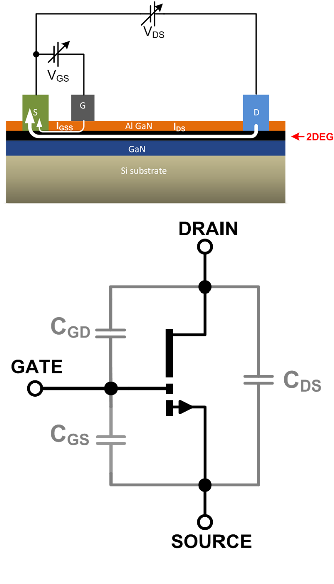
Figure 2. Topology for e-mode GaN devices is conceptually similar to silicon MOSFETs.
The same circuit techniques used to drive traditional silicon MOSFETS can also be used with e-mode GaN HEMTs. In other words, the GaN device works much like a silicon MOSFET, only with much better switching and circuit performance. Additionally, GaN E-HEMT devices are closer to the “ideal switch” in power electronics applications because they do not have an intrinsic parasitic body diode as do silicon MOSFETS. Thus, there is no need for anti-parallel diodes.
Advances in E-Mode GaN
The desire for benefits arising from e-mode GaN devices has yielded advancements in e-mode GaN HEMT technology, and can be seen in GaN Systems E-Mode product line. The benefits of these advanced devices include a more robust gate structure than similar devices, no DC holding current, and no complex gate diode PN junction. They switch on average four times faster and turn off at least two times faster than comparable devices on the market. By spending less time in the linear region, efficiency is greatly improved. Also, their lower gate capacitance means less energy is consumed driving the gate. The resulting energy savings applies right to the bottom line of increased power converter efficiency.
Not only can E-HEMT GaN devices upgrade many existing topologies, they enable new applications that were not possible with traditional options. For example, E-HEMTs can replace IGBTs in half-bridge hard-switching power converter circuits with drastic improvements in circuit performance. Moreover, E-HEMT GaN devices enable innovative topologies not possible with MOSFET devices such as the bridgeless totem pole topology (Figure 3). Silicon MOSFETs could never be used for these applications due to the limitations of QRR.
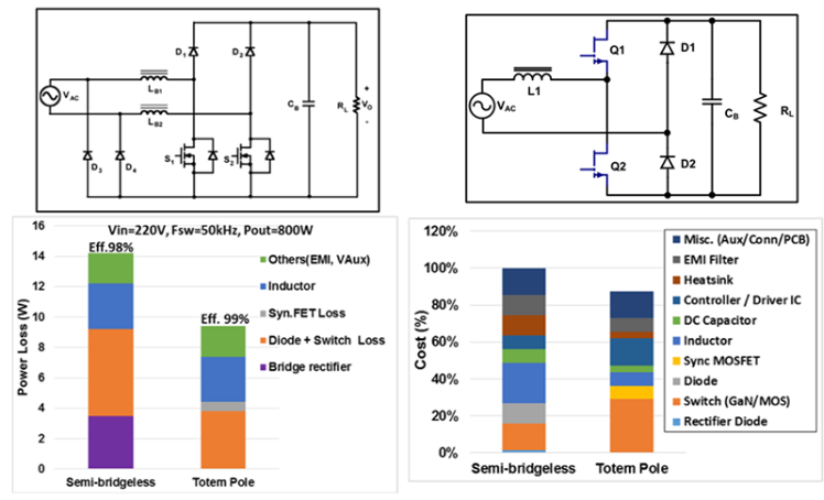
Figure 3. The Totem-pole topology possible with E-HEMT GaN delivers dramatic improvements in efficiency and size.
Benefits for Power System Design
As has often been observed, semiconductor advances are either the result of improvements in process or packaging. In the case of the GaN Systems E-Mode devices, both areas are evident. The work being done to increase the benefits of E-HEMT GaN devices include embedded die and advanced packaging and co-packaging of drivers and the GaN switches to minimize parasitic interconnections – offering functional modules and more.
The resulting benefits of using this are many:
These device attributes translate to reduced size and weight benefits; devices can be a quarter that of a silicon designs, which leads to lower system cost and increased efficiency, all of which results in lower total cost of ownership for the end user.
Industry Roadmap and Market Trends
Reducing size and weight, while increasing performance (including power density), is now a requirement for power system applications. In the transportation sector, for instance, some automakers have announced that they will discontinue internal combustion engines within the next several years. This means that the infrastructure for electric transportation systems will need to be rapidly built-out. Moreover, electric vehicle rapid-recharging stations will need extremely efficient power electronics as will the on-board power electronic systems in vehicles themselves.
Also, one of the biggest needs for efficiency will be in server farms and data centers, which are being built out at a tremendous rate to serve the insatiable need for communications and storage for big data, IoT, and general internet traffic. In addition to saving energy, any increases in power density and efficiency are especially coveted since they translate directly into lower utility costs.
It’s clear that the needs of the power electronics market aligns with the demonstrated benefits of GaN devices when incorporated into power electronics systems.
In Part 2, we will further explore the technical details of applying e-mode GaN devices to effect innovative and highly efficient power conversion topologies.
Gallium nitride (GaN) and advanced silicon technologies offer sizeable power density enhancements compared to legacy solutions. But greater density presents thermal management challenges. Designers typically de-rate performance, add bulky heat spreaders or utilize active heat dissipation to ensure resilience and longevity. According to Element Six, CVD diamond could offer more effective, smaller and less complex solutions for 5G and other high power electronic systems. By: Firooz Faili, Head of CVD Thermal Products at Element Six
Diamond possesses a remarkable set of properties, making it the most effective material for solving thermal management problems. Microwave-assisted undoped CVD (chemical vapor deposition) enables control of grain size, grain purity and grain interfaces to generate high-quality, high repeatability, polycrystalline diamond at the targeted thermal conductivity level needed for particular applications. Commercially, CVD diamond is readily available in six different grades with thermal conductivities ranging from 700 to 2000 W/mK and bulk resistivity from 0.001 m for doped diamond to 1012 m for undoped diamond.
A crucial element in developing disruptive technology is the control of basic building block engineering. The use of CVD grown diamond as a high-performance heat spreader can ensure the effective performance of a wide range of disruptive electronics from GaN solid state RF X-band PAs to advanced ASICs to laser diodes. Naturally, understanding the fundamentals of the science and engineering of the thermal properties of grown diamond is an essential part of this process.
Element Six, part of the De Beers Group of companies, has spent over 25 years in developing, understanding and characterizing CVD technology and CVD diamond material, operating worldwide with primary manufacturing facilities in the UK and US.
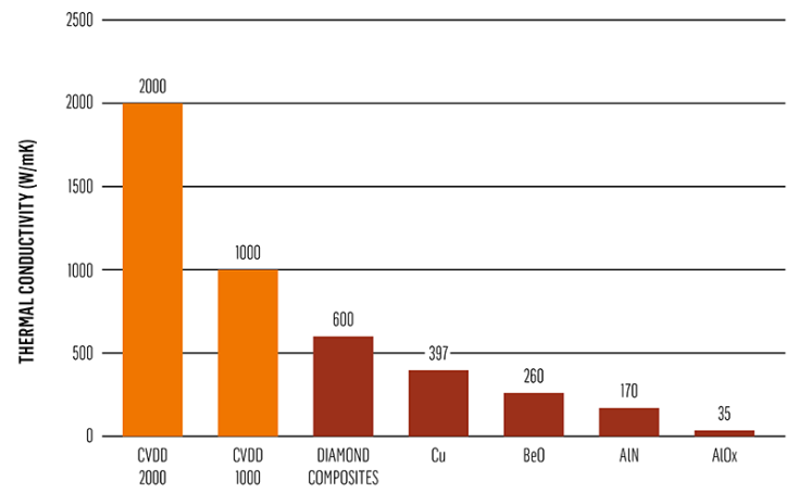
Fig. 1: Comparison of CVD diamond with ‘traditional’ heat spreading materials
Diamond, the ultimate substrate material
In designing a thermal management system, it is important to consider both the material and the application methodology to minimize channel temperatures and deliver long-term device operation. To date, the integration of SiC (400 W/mK) substrates with GaN has provided the best option for GaN HEMT and MMIC technology for high power applications. However, despite the use of SiC substrate, adequate heat spreading is still the limiting factor in determining the maximum power dissipation for GaN based electronics. As such, the path to long-term reliability is often achieved by de-rating the maximum power dissipation. A far better heat spreading solution incorporating CVD diamond (2000 W/mK) has the potential for a factor of 3× or greater increase in power density relative to current state-of-the-art GaN devices. (Figure 1 compares performance of various substrate materials.)
While GaN-based electronics are capable of delivering ultrahigh current and power density performance, the failure of many high-end electronic systems is directly attributable to the lack of adequate thermal management.
Semiconductor devices continue to increase in power density. For high power RF and Optoelectronics, using CVD diamond enables devices to run at increased power levels without raising junction operating temperature, thereby delivering longer lifetimes and better reliability.
An packaged RF application example
To demonstrate the impact of a diamond heat spreader in a practical example, an RF-amplifier design was analyzed. In this example, a packaged VDMOS (Vertical Diffused Metal Oxide Semiconductor) power amplifier was initially made with a BeO (Beryllium oxide) heat spreader on a CuMo (Copper / Molybdenum) flange. The end-user was interested in lowering the overall thermal resistance of the system design while also avoiding the use of BeO due to its toxicity.
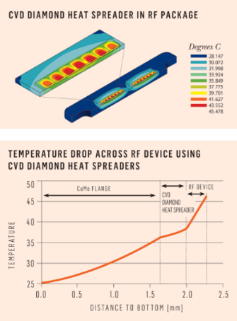
Fig. 2
Figure 2 demonstrates the temperature profile junction-to-case for one of the optimal designs derived from this modelling. The CVD diamond heat spreader solution was found to have 30% lower thermal resistance at 0.300 mm in thickness at a thermal conductivity of 1000 W/mK (the original solution used a 1.00 mm thick BeO heat spreader). The lower thermal resistance of the diamond heat spreader has led to this device functioning with better RF linearity performance and with improved reliability due to its reduced junction temperature.
Boron doped, electrically conductive CVD diamond, a unique material for high frequency packaged electronics
As an electrically conductive heat spreader, thick, boron doped diamond (BDD) with metallic conductivity (0.05 Ω-cm resistivity) is an ideal replacement for the commonly used metal/diamond configuration or other heat spreaders such as copper, copper/refractory or copper laminate. Mounting of RF/microwave devices on a BDD heat spreader enables better isolation of the ground plane at below 1.5 GHz, and in reduction of conductive losses at and above 1.5 GHz due to the increased skin depth.
RF current flows on a metal surface and for typical metals (Cu or Au) at above 1.5 GHz the already very thin skin depth continues to decrease with increasing RF frequency. The decrease in skin depth results in a surface resistance increase and hence increasing conductive losses. Above 1.5 GHz, in comparison to Cu and Au, BDD has nearly two orders of magnitude greater skin depth at the same RF frequency (Figure 3). The higher conduction cross-section of BDD not only enables better RF performance by improving the ground-plane isolation, but also in reducing conductive losses at higher frequencies.
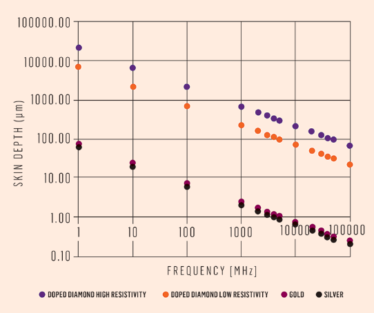
Fig. 3: Skin depth for conductors at increasing operation frequency
Boron doped diamond heat spreader at various frequencies
Using thick BDD with metallic conductivity, instead of the standard metal/diamond enables better isolation of the ground plane below 1.5 GHz by increasing the skin depth.
The metallic-like heat spreader reduces the slow wave mode and the capacitive coupling between ground planes found in metallised dielectrics below 1.5 GHz. It should be noted that a gold metallization might still be beneficial in reducing the electrical resistance of the BDD substrate.
For electronic applications operating below 1.5 GHz, the standard metallized diamond heat spreader (1000-2000 W/mK) may introduce unwanted couplings between grounds due to the capacitive coupling of the metallized ground plane at this frequency range. In this region it is functionally beneficial to sacrifice some of the ultra-high thermal conductivity of diamond by making it electrically conductive.
CVD diamond, the future of high frequency resistive components
Though the frequency range of 5G network system is not yet decided, the standardization of 5G network system is well underway.
While the network communications (between each base station) system will be using the 28-30 GHz frequency range to achieve a high data rate of exchange, it is expected that 6-8 GHz and/or up to 10 GHz will be used for personal cellular connections. On the amplifier front, GaN-based HEMTs appears to be the only solution for high power/high frequency operation in the 28-30 GHz range.
Currently most major network system manufacturers (Ericsson, Nokia, Huawei, etc.) are focusing on a method of phased array (128 channel) communication for 5G in the 6-8 GHz frequency range. With increasing frequencies there is a need for component size reduction, which results in increasing demand for more efficient thermal management. CVD diamond is uniquely positioned to provide the solution not just for amplifiers, but also as a resistive component for devices such as isolators, limiters and phase shifters.
The millimeter wave market demands solutions that offer gigahertz performance at high output power levels. With the designation of the operating spectrum for 5G at above 6 GHz, and high-performance phased arrays radars operating in the X- and Ku-bands, there is significant drive for passive components able to handle high power density at higher frequencies.
To date beryllium oxide (BeO) and aluminum nitride (AlN) have been the preferred substrates for high power RF resistors. These ceramic materials have relatively high thermal conductivity and enable resistors to handle tens to hundreds of watts when operating at L- and S-bands (1 4 GHz). However, when operating from X band up to Ku band (8 30 GHz), the trade-off between maximizing the dissipated power and reducing resistor parasitic effects leads to a diminished ability to dissipate a few watts when using BeO or AlN substrates. This limitation in management of power at higher frequency will become a bottleneck for extending high power applications above S-band. What is proposed here is an enabling solution for RF resistors capable of operating above 8 GHz while handing over 100 W by using CVD diamond as the resistor substrate.
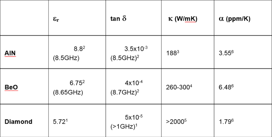
Fig. 4
Figure 4 summarizes the values of the key parameters affecting performance for the different high thermal conductivity substrates used in RF resistors. It is evident that AlN, with the highest permittivity and the lowest thermal conductivity will perform worse than BeO, and that diamond—having the best combination of low permittivity and highest thermal conductivity—would excel as a high frequency resistive substrate. Diamond’s permittivity is ~15-35% lower than those of BeO and AlN respectively and remains stable with changes in frequency and temperature, varying by only 5% from low frequencies up to tens of GHz, and only shifting by 730 ppm/°C from room temperature up to a few hundreds of degrees centigrade.
Temperature is also important when considering thermal conductivity. At 125°C the thermal conductivity values for AlN and BeO are reduced by 30-40% compared to performance at room temperature. Thermal conductivity of the purest single crystal diamond may exceed AlN and BeO by a factor of ~10-15, which roughly means that a resistor using diamond should be able to handle 10-15 times more power. When considering polycrystalline diamond as a resistive substrate with thermal conductivity ranging from 1000 W/mK to 1800 W/mK, a 4-8x improvement in performance over that of AlN and BeO could be realized.
A word on cost
A subject worthy of an extended article by itself, the cost of diamond heat spreader technology should be viewed from two primary angles. Firstly, a consideration of cost should be made when standard heat spreaders cease to perform in cooling high power density devices in RF, microwave and ASICs. Secondly, and perhaps more importantly, is that the cost of performance improvement could and should always be optimized multi-dimensionally. The ratio of device to spreader area, the spreader thickness and the CVD diamond heat spreader thermal conductivity all play primary roles in controlling thermal resistance and cost. As a result, it is imperative to follow a proper performance/cost model to optimize diamond heat spreader benefits.
Summary
Significant thermal-management improvements within electronic systems can be realized by using CVD diamond. The integration is relatively straightforward as CVD diamond can be a direct replacement for AlN (Aluminium nitride), BeO (Beryllium oxide) or other advanced ceramics. Attention to detail at the interfaces is important to keep overall thermal resistance low, thereby optimizing the effectiveness of the diamond.
Through improved synthesis technology, advanced processing and on-going cost reduction efforts, CVD diamond has become a crucial enabler as a heat spreader and heat dissipater for high power density RF applications. It is expected that this trend will continue in the years to come, in line with the ever-increasing need for smaller and more powerful electronic devices and systems, including the growing demand for defense as well as upcoming 5G wireless applications.
References
[1] A. Ibarra et al, Wide frequency dielectric properties of CVD diamond, Diamond and Related Materials, 6, 856-859 (1997).
[2] W.B. Westphal and A. Sils. Dielectric constant and loss data. Vol. 72. No. 39. Air Force Materials Laboratory, Air Force Systems Command, (1972).
[3] J. E. Graebner et al. Report on a second-round robin measurement of the thermal conductivity of CVD diamond. Diamond and Related materials 7.11 1589-1604, (1998).
[4] G.P. Akishin et al. Thermal conductivity of beryllium oxide ceramic. Refractories and Industrial Ceramics 50.6 465-468, (2009).
[5] L. Wei et al. Thermal conductivity of isotopically modified single crystal diamond. Physical Review Letters 70.24 3764. (1993).
[6] G.A Slack & F. Bartram. Thermal expansion of some diamondlike crystals, Journal of Applied Physics 46.1 89-98. (1975).
Many nations have mandated the phase-out of internal combustion engines in the coming decades to meet global greenhouse gas reduction targets. Electric vehicle (EV) performance can be optimized by utilizing advanced design and simulation tools that save manufacturers time and money. By Guilherme Tondello, Creative Solutions, and Puneet Sinha, Mentor-A Siemens Business, Mechanical Analysis Division
Germany, Britain, Norway, The Netherlands, and France have announced bans on new internal-combustion engines within the next 5 to 15 years; other countries are calling for gradual phase-outs of fossil fueled vehicles, or increasing the share of electric vehicles (EVs) and hybrid EVs on their roads by 2050. In the United States, this movement is being led by California. China is expected to be the largest market for electrical vehicles (EVs). Predictions are that by 2040, 54% of new car sales and 33% of the global car fleet will be electric [1].
Some of the important challenges in EV development and sales are getting more than 200 miles out of a charge; pricing below (USD)$40,000; fast charging—meaning less than 30 minutes recharging time for an 80% charge; increasing fuel efficiency over a larger range for hybrids, and the development of autonomous vehicles. Many countries and major cities are pushing for the electrification of not just cars, but also industrial, public service, and mass transportation vehicles.
For the electric powertrain, the engineering focus is on the price and size of battery packs, motor efficiency that effects driving range, and the trade-off between drive range or performance (balanced against) ever-increasing driver experience requirements and features. Energy storage needs to be designed so that it obtains the required energy and power density in each battery cell as well as the overall pack. The pack has to be thermally regulated so that it won’t overheat. Energy storage has to be monitored and optimized while driving.
The motor and power electronics need to be optimal for the architecture, weighing efficiency vs. performance vs. cost. Here also, thermal management and reliability are important issues. The power electronics need to be reliable over a wide range of operating temperatures, and design is a challenge with the inverter and motor inside a single casing.
The skills of computational fluid dynamics (CFD) experts traditionally have been necessary for electric powertrain, as well as component-level design, and to expose underlying limiting phenomena. However, relying solely on CFD experts today can result in either slower deployment or under-achievement of the expected design.
A new approach, where automotive designers can use the CFD tools easily as early as possible in the design phase to evaluate prototype designs and optimization, is gaining traction among OEMs and Tier-1 suppliers. This front-loading, designer-centric approach rests on three elements: 1) CAD-embedded CFD that allows complex simulations to be done by non-CFD experts in the native CAD environment of designers; 2) simulation automation and a built-in database to allow engineers to achieve reliable and accurate results; 3) seamless integration with electronic design automation (EDA) and system simulation tools. Using this approach, we have seen results that reduce the time and cost as much as 60 percent [2].
Battery-Pack Design and Prototyping Case Study
Let’s look at a real-life example of where this approach has shown immediate benefits. The Mobilis company in Brazil builds EVs for recreational use in rough road and ambient conditions [3]. The vehicles are air-cooled with 4-kW/h battery packs. The company obtains battery packs, or battery cells, from their suppliers, and then they integrate them into their vehicle designs (Figure 1).
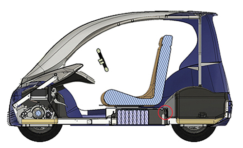
Figure 1: Battery pack housed at the floor of a Mobilis vehicle.
The design engineers needed to figure out what kind of geometry they would need with this particular battery pack so that the vehicle could fulfill its cooling objective in harsh climatic conditions, compared to the manufacturer’s nominal recommendations. Operating temperatures that are more uniform with lower maximums result in longer battery life. Evaluation of designs on battery thermal behavior with implications for pack reliability in real-world operation is ideally suited for using a CAD-embedded CFD simulation approach.
The original battery pack design (Figure 1b) consisted of one inlet and outlet for air with an outlet port on the side that had a smaller diameter than the inlet port. In their calculations, they made an assumption about the turbulent flow for the aluminum base plate (enclosure of the battery pack) based on the likely interactions between the air and uneven geometry underneath the vehicle. Air-flow distribution within the pack has a strong effect on the battery’s thermal behavior.
Assessing Thermal Behavior of both Original and New Designs
Analysis of the original design as built into the first prototype showed that the air outlet location wasn’t optimal for their needs; the constrained space between the cells and the air outlet port rendered insufficient air flow. The temperature reached an unacceptable 84 °C, so the engineers decided to change the geometry of the pack to increase the air flow.
After design iterations using simulation and analysis, they added another inlet and outlet, shifted the air-outlet ports to the side, and increased the outlet ports’ diameter to match the inlet ports. Figure 1c shows the new CAD design, and Figure 2 shows the air flow (pressure distribution) in the redesigned pack compared to the original.
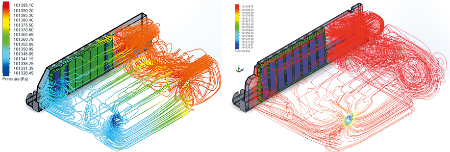
Figure 2: Air-pressure distribution inside the redesigned battery pack (left). In the original design (right), the constriction at the outlet is clearly visible.
The engineering team was able to eliminate flow constriction near the outlet and had fewer areas of flow stagnation compared to the original design. Also, the new design improved the air-flow rate in the narrow area of battery cells and battery pack enclosure, which helped convective heat transfer. Figure 3 shows the resulting temperature distribution in the new pack. The maximum temperature was 54 °C (compared to 84 °C for the original design), which was well within the cell manufacturer’s maximum recommended temperature.
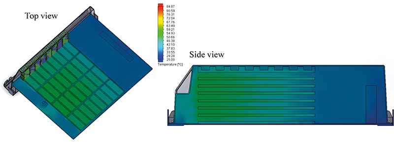
Figure 3: Temperature distribution in the redesigned battery pack for nominal operating conditions. Maximum temperature in the pack’s new design is 54 °C.
Simulating Extreme Operating Conditions
The next step was to simulate the thermal response of the redesigned battery pack under critical conditions (Table 1), compared to “normal” conditions, which they considered to be a warm day at 30 °C, carrying a medium load, at slow speeds (25 kph or 15 mph). Critical is defined as extreme operating conditions that the vehicle may be exposed to for short periods of time, but is not designed to operate in continuously, using three times more power per cell with half the available airflow compared to normal.
Their analysis showed that the redesigned pack would reach unsafe temperatures as high as 110 °C, if the vehicle was operated under such critical conditions continuously. They wanted to be able to estimate temperature ramp up in the battery pack once it was subjected to these extreme conditions, and if it would be enough that the system needed to react.
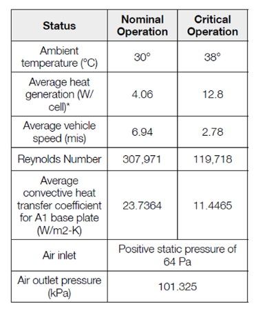
Table 1: Parameters used to compare the battery-pack design performance under “normal” recommended versus critical operating conditions.
Under such conditions, the battery pack could operate for approximately 78 minutes from rest conditions before the battery-pack temperature rose beyond the maximum recommended temperature of operation (60 °C). Figure 4 shows the temperature rise in the battery pack when subjected to these critical operating conditions. Because of the battery’s large thermal mass, this slow temperature rise rate provided enough time to take necessary actions to avoid damage to the battery pack that would limit its life; this design change was deemed a success.
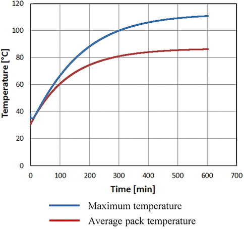
Figure 4: Temperature rise in the battery pack over time when subjected to critical operating conditions.
Summary
Working with a consultant at Creative Solutions, Mobilis engineers leveraged the CAD-embedded computational fluid dynamics (CFD) software, FloEFD, for optimizing their battery-pack design. Starting with an initial CAD design of the battery pack, they simulated dozens of scenarios to explore the battery thermal behavior with changes in the battery’s design. Through this process, the engineers reached an optimized battery-pack design much more quickly than if they had needed to send out their models for CFD analysis using the traditional approach in which significant, specialized engineering efforts would have been dedicated to CAD-to-CFD translation.
Through these simulations, they were assured that the cooling system would be adequate for the harshest cases, such as driving on a long steep uphill with the vehicle loaded, when the asphalt is hot, or starting the vehicle when it has been parked outside on a sunny summer day. The simulations were instrumental to understanding how use-conditions could negatively affect battery life and which operating conditions should be avoided by customers, as well as for devising strategies to mitigate liability issues that can be caused by misuse or random unpredictable system failures.
References
1. “New Energy Outlook 2017” by Bloomberg New Energy Finance
2. John Parry, “State of the Art Automotive Thermal Design by DENSO,” Engineering Edge https://www.mentor.com/products/mechanical/engineering-edge/volume2/issue1/DENSO--State-of-the-Art-in-Automotive-Thermal-Design
3. Vitor Straub, “CAD-Embedded Battery Pack Design Optimization for Mobilis Electric Vehicle,” Engineering Edge https://www.mentor.com/products/mechanical/engineering-edge/volume6/issue2/cad-embedded-battery-pack-mobilis-electric-vehicle
Advanced semiconductors now support previously unattainable efficiency and power density. But these devices place high demands on test and measurement (T&M) equipment; oscilloscopes with isolated input channels are ideal solutions with wide-ranging analytical abilities. By: Dr. Markus Herdin, Product Manager for Oscilloscopes, Rohde & Schwarz, Munich
Very short rise times and low losses are two major advantages of power transistors based on silicon carbide (SiC) and gallium nitride (GaN) semiconductors. These advantages translate into higher efficiency and power density. At the same time, advanced semiconductors of this kind allow high electrical strength, which is critical when designing high-power converters. This applies especially in the case of electrical drives and power converters. However, the specified voltage limits for the semiconductors must be strictly followed due to the risk of destruction.
Users are thus faced with some new challenges:
Special probes are too expensive
Large bandwidth and high common-mode rejection can be attained using optically isolated probes, for example. However, special probes of this kind typically cost much more than the actual oscilloscope, and the costs are multiplied if multichannel measurements are required. In addition, the input voltage range of these probes is limited so that only selected measurements are possible. For many developers of power electronics, this is simply not a viable option.
The cost-effective alternative
Advanced oscilloscopes with isolated input channels provide an economical yet effective alternative. The portable R&S Scope Rider is a good example of such an instrument. It has four isolated input channels that can be used to perform differential measurements on potential differences of up to 1000 V (RMS) – without requiring costly differential probes. With 500 MHz bandwidth, it is well suited for measurements on advanced SiC and GaN semiconductors. Moreover, it can be battery-powered for mobile applications. Unlike other oscilloscopes with isolated inputs, the R&S Scope Rider provides analysis capabilities on the level of laboratory oscilloscopes, including an extremely fast acquisition system with an acquisition rate of up to 50,000 signal waveforms per second, flexible trigger functions and a wide range of automatic measurement functions.
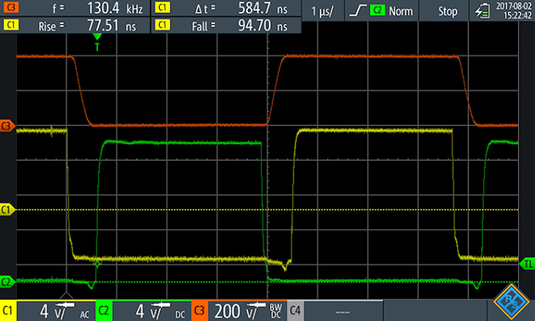
Fig. 1: Measuring the gate source (C1, C2) and output voltage (C3) of a resonant converter; all figures and graphic representations in this article are courtesy of Rohde & Schwarz (R&S)
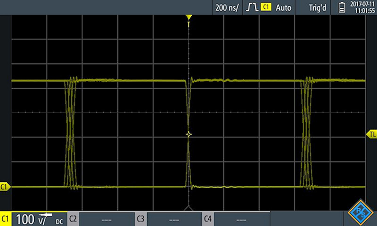
Fig. 2: Measuring the switching cycle of a GaN-based power factor correction (PFC) output stage; source: R&S
Correct connections are essential
Performing high-quality measurements on power electronics requires the right test instrument and the right probe as well as careful attention to the correct connection. Passive probes are ideal for measurements with an oscilloscope that has isolated input channels. Here, the contacts with the signal and ground connections must be as short as possible in order to minimize ringing and achieve the highest possible common-mode rejection. Ground springs generally help to ensure optimal contacting when using a passive probe. However, when measuring hazardous live voltages, prefabricated contact points must exist for safety reasons. Normally, small conductor loops are soldered onto the contact points so the passive probes can be connected there. In certain situations, a BNC connector can also be installed as an alternative. BNC adapters can then be used with the probe in order to achieve a nearly ideal connection.

Fig. 3: Prefabricated conductor loops for safe measurement of hazardous live voltages using passive probes and an oscilloscope with isolated inputs; source: R&S
Differential probes can generally be connected arbitrarily in the circuit. However, when making measurements with isolated input channels, the exact points where the signal conductor and the ground are connected are very important. The unbalanced design used in isolated input stages results in much lower capacitance between the signal path and earth potential compared to what exists between the ground path and earth potential. In order to obtain satisfactory measurement results, the signal path should be connected to the appropriate measurement point.
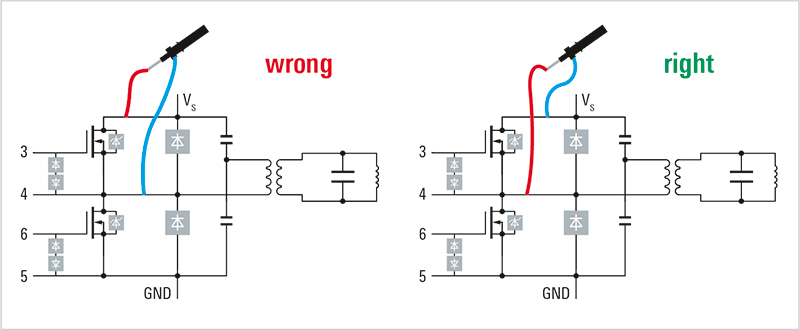
Fig. 4: For measurements with isolated input channels, the signal conductor should always be connected to the appropriate measurement point; source: R&S
Critical parameters
Converters for electrical drives typical operate with clock frequencies in the range from 10 kHz to 100 kHz. In order to make safe measurements on converters of this sort, the critical parameters include the maximum voltage of the measuring system as well as the "derating" vs. frequency. As the frequency increases, the maximum permissible voltage decreases at the measurement input or between the ground potential of the measuring system and earth potential. If this voltage is exceeded, the user can be endangered. The R&S Scope Rider allows measurements with full signal amplitude up to 100 kHz, making the instrument well suited for this application.
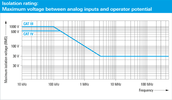
Fig. 5: Derating of the maximum voltage between the oscilloscope input and earth potential in case of the R&S Scope Rider. Clock frequencies up to 100 kHz can be safely measured with the maximum permissible input voltage; source: R&S
If the DUT is also connected to the electrical installation, the measurement category must be taken into account too. Depending on where the DUT is connected in the electrical installation, the measuring system must tolerate different levels of voltage peaks on the input channel without endangering the user due to flashovers or short circuits. As the location gets closer to the building connection for the electrical installation, higher levels of voltage peaks can occur, thereby increasing the required overload protection. An isolated oscilloscope in category 4 (CAT IV rating) provides the necessary degree of safety. The R&S Scope Rider has overload protection of up to 8000 V and is thus appropriate for 600 V (RMS) in a CAT IV environment or 1000 V (RMS) in a CAT III environment.

Fig. 6: Measurement categories in line with EN 60664-1; source: R&S
Additional functions simplify everyday measurements
Cutting-edge oscilloscopes offer a number of functions that greatly simplify everyday measurements. For power electronics, this includes automatic measurement functions for calculating the apparent, active and reactive power, flexible triggering capabilities to allow selection of specific signal elements in a switching operation, and a measurement data logger or history function for long-term monitoring of selected measured values or signals.
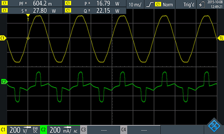
Fig. 7: Automatic measurement functions calculate the apparent, active and reactive power as well as the power factor from the measured voltage (channel 1) and current (channel 2); source: R&S
Another useful analysis function is provided by the harmonic analyzer. Current and voltage harmonics are unwanted spurious products of converters. These harmonics must lie within specified limits in order to avoid a negative impact on the power quality. Other important parameters include the phase relationships between the different harmonics as well as the total harmonic distortion (THD).
The R&S Scope Rider provides these measurement functions thanks to its harmonics analysis function. Up to four channels can be simultaneously and automatically evaluated, displayed and monitored with respect to predefined limits if necessary.
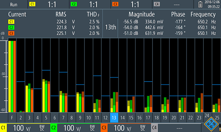
Fig. 8: Harmonics analysis of a three-phase 100 V signal. The blue lines show the current limit value in line with EN 50160. The 13th harmonic and its characteristics are highlighted; the highlighted levels for the three channels lie between –56.5 dB and –51.0 dB; source: R&S
In order to provide maximum safety for hazardous test situations, the R&S Scope Rider (R&S RTH) can be remotely operated via WLAN to fully decouple test instrument operation from the DUT.

Fig. 9: In especially hazardous test situations, the R&S Scope Rider can be remotely operated via WLAN; source: R&S
Summary
Developers have already come to appreciate oscilloscopes with isolated input channels as a powerful yet cost-effective alternative for safely performing measurements on power electronics modules. Thanks to advanced frontend technology, up to 500 MHz bandwidth and powerful signal processing, these oscilloscopes are now also appropriate for measurements on circuits with GaN- or SiC-based semiconductors. The R&S Scope Rider from Rohde & Schwarz is an impressive representative of this class and is also well suited for classic oscilloscope applications due to its wide range of analysis capabilities.
Author: Dr. Markus Herdin is product manager for oscilloscopes at Rohde & Schwarz in Munich.
More information: www.rohde-schwarz.com/rth.
Silicon transistors are tipped to offer diminishing returns at the 7 nm CMOS node and beyond. Can InGaAs vertical nanowire MOSFETs step in and maintain the march of Moore’s Law? By Xin Zhao, Wenjie Lu, Alon Vardi and Jesús A. Del Alamo from Massachusetts Institute of Technology
The silicon MOSFET is fulfilling the moto ‘smaller is better’. Continuous reductions to its size for five decades have enabled it to keep pace with Moore’s Law, while underpinning a microelectronics revolution that has transformed virtually every aspect of human life.
But scaling can’t go on forever. As the transistor shrinks into the nanometre regime, smaller is not always better. Simply reducing dimensions even further will cause severe short-channel effects to will escalate, impairing device performance. To overcome this issue, the silicon IC industry has switched from planar device geometry to a FinFET structure (see Figure 1). The new architecture, introduced at the 22 nm mode, has a conducting channel residing in a thin fin of semiconductor, which sticks out of the wafer surface. This design provides a high degree of electrostatic control, enabling the scaling of the gate length to very small dimensions. Today, the width of this fin in state-of-the-art FinFETs can be as narrow as 7 nm – and from here on, it will be a grand challenge to keep shrinking lateral dimensions, so more devices can be packed in a given footprint.
A characteristic shared by planar MOSFETs and FinFETs is that current flows parallel to the wafer surface. In contrast, in the power electronics industry, engineers manufacture vertical structures, with current flow perpendicular to the wafer.
One key advantage of the vertical geometry is that it decouples aggressive footprint scaling from gate length and contact length scaling. Thanks to this, the footprint can be trimmed again and again without giving rise to short channel effects.
Immunity to short channel effects is particularly prevalent in nanowire transistors, a class of device that sports a unique gate-all-around geometry.
The vertical nanowire transistor has the potential to propel Moore’s law further into the future than any other device structure.
Impeccable InGaAs
Many groups have already made vertical nanowire MOSFETs that are based on silicon. But unlike their planar counterparts, the performance is rather unimpressive. Carrier mobility in silicon is not that high, so it is common practice to increase this by introducing strain into the device. But for the vertical nanowire MOSFET, no efficient methods exist for strain engineering the channel.
Far more promising is the family of III-V compound semiconductors, which has attracted considerable interest to advance logic CMOS. The jewel in the crown is InGaAs, which has an outstanding electron velocity. This ternary has held the key to fabricating record-breaking HEMTs and HBTs. In addition, InGaAs is a perfect candidate for the channel material in vertical transistors. At MIT we are using it in that manner, and breaking new ground by scaling the vertical nanowire MOSFET to far smaller dimensions than our peers.
By adjusting its composition, InGaAs can cover a wide range of lattice constants, effective masses and bandgaps, allowing its electrical properties to be finetuned. What’s more, when InGaAs is paired with other III-Vs, such as InAlAs and InP, this enables flexible, powerful bandgap and strain engineering.

Figure 1. The evolution of logic transistor architecture, from a planar device to a vertical nanowire MOSFET (note that SOI is short for silicon on insulator).
Note that the vertical channel configuration is a perfect fit for III-Vs, because carrier flow takes place in the direction of epitaxial growth. This opens up, for the first time, the possibility of band structure engineering along the carrier transport direction, expanding device design opportunities – they can include leakage current reduction, through bandgap engineering of the drain and source; and strain engineering, to boost both the carrier density and the velocity.
Interest in III-Vs goes beyond its high speed advantage. When III-Vs are integrated with silicon, systems can be produced that combine logic, terahertz sensing, imaging and communication, as well as optical functions, opening the door to numerous novel applications.
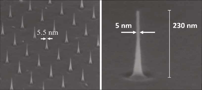
Figure 2. Scanning electron microscopy images of an InGaAs vertical nanowire array (left) after seven digital etch cycles in 10 percent H2SO4 in methanol. The 5.5 nm diameter nanowire yield is 90 percent. On the right is an exemplary single InGaAs vertical nanowire with a diameter of 5 nm and aspect ratio of over 20.
Armed with its excellent set of attributes, InGaAs has recently been used to demonstrate planar MOSFETs and FinFETs with impressive characteristics. Fabrication has drawn on: the development of highly scaled metal-oxide-semiconductor gate stacks, which have excellent interfacial characteristics; ohmic contacts with a low contact resistance; and very tight, self-aligned designs. One of the upshots of these efforts is that they have laid a solid foundation for advancing InGaAs vertical nanowire MOSFETs.
Shrinking InGaAs nanowires
The performance of the vertical nanowire MOSFET is governed by the quality of the nanowire. At the point of insertion into the CMOS roadmap, vertical nanowire transistors must have a vertical nanowire with a diameter of less than 10 nm, as well as vertical, smooth sidewalls.
Given these requirements, it is of no surprise that the formation of the nanowires is a critical issue. One option is the bottom-up approach, which involves the growth of compound semiconductor heterostructures, using either catalyst nanoparticles or patterned oxide masks as a template. This approach, which minimizes threading dislocations via two-dimensional confinement, is attractive because it enables the relatively straightforward integration of III-Vs on a silicon wafer. Note that engineers adopting the bottom-up approach have several options, including the vapour-liquid-solid method, selective-area epitaxy and template-assisted growth.
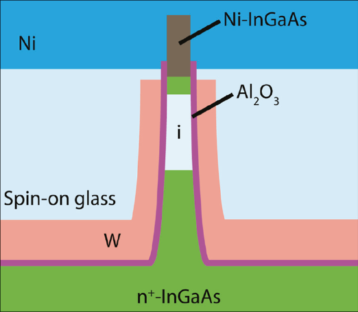
Figure 3. MIT’s InGaAs vertical nanowire MOSFETs features an Al2O3 dielectric and a nickel-InGaAs top contact.
Approaching the challenge from the opposite direction is the family of top-down techniques. Here, the key technology is reactive ion etching, an industrystandard process that creates high-aspect ratio structures, thanks to its high degree of directionality.
Prior to our work, top-down techniques could only define micrometre-scale structures in InGaAs.We have smashed through this barrier, using a combination BCl3, SiCl4 and argon to etch nanowires with diameters as thin as 15 nm and aspect ratios in excess of 15.
A key breakthrough associated with our work is the use of a ‘digital etch’, which provides precise trimming of the nanowire diameter and smoothing of the sidewalls through a highly controlled, self-limiting chemical process. Additional merits of this process are the preservation of nanowire shape and an improvement to the electrical quality of the sidewalls.
We have discovered that it is of paramount importance to select an appropriate solvent for the acid that is used in the digital etch process during the oxide removal step. Using water allows precision dimension engineering, as well as successful mitigation of surface damage that is introduced during a dry etch. However, a water-based approach also leads to the destruction of vertical nanowires when their diameter is 10 nm or less. This is caused by the high surface tension of the water-based acid.
For our work, alcohol is a better option. Making the switch greatly improves the mechanical yield for nanowires with diameters below 10 nm. By turning to 10 percent H2SO4:methanol, we can use digital etching to produce a yield of 90 percent for nanowires with 5.5 nm diameter (see Figure 2). Close inspection of nanowires within this array reveals that we have produced structures with a 5 nm diameter and aspect ratio over 20. To our knowledge, this sets a new benchmark for miniaturization of the InGaAs vertical nanowire. Note that there is a vertical sidewall towards the top of the nanowire, where active device layers are present.
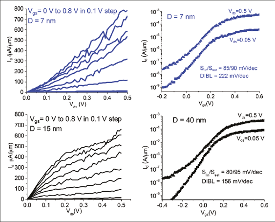
Figure 4. Subthreshold and output characteristics of InGaAs vertical nanowire MOSFETs with nickel contacts and diameters of 7 nm (upper row) and 15 nm (bottom row). All figures of merit are normalized by the nanowire periphery.
One of the big challenges with vertical nanowire transistors with diameters below 10 nm is the addition of electrical contacts. For non-alloyed contact metals, such as molybdenum and tungsten, full depletion under the contact can only be avoided by using a mushroom-shaped top contact region – and this creates a wider nanowire tip. A top-heavy structure results, which is mechanically fragile, adding considerably to process complexity. To address this, we use nickel-alloyed contacts. Nickle reacts with InGaAs to form a highly conducting NiInGaAs metallic phase.
Record performance
Our vertical nanowire MOSFETs are made out of InGaAs, and consist of an intrinsic channel region sandwiched between two n+ contacts (see Figure 3). The gate stack includes high-κ dielectric Al2O3, deposited via atomic-layer-deposition, onto which tungsten is sputtered. To provide isolation between drain, gate and source electrodes, two steps of planarization and etch back are undertaken using spin-on glass, before nickel is sputtered as the top contact metal. Fabrication is completed with a forming gas anneal at 200 °C, to drive a reaction between nickel and InGaAs that forms a top contact. In addition, this final step improves the interface between the oxide and the semiconductor.
Electrical measurements on a typical vertical nanowire MOSFET, which has a diameter of 7 nm, reveal an on-off ratio close to 105 at a drain-source voltage of 0.5 V. A record peak transconductance of 1.7 mS/μm at an on-resistance of 1100 Ω μm is obtained, highlighting the strength of this device to achieve high-performance computing. The minimum linear sub-threshold swing, measured at 0.05 V, is 85 mV/decade, while the saturated sub-threshold swing, measured at 0.5 V, is 90 mV/decade. These values indicate reasonable sidewall and interface quality. A drain-induced barrier lowering of 222 mV/V is observed.
The output characteristics for this 7 nm-diameter device do not show current saturation. This indicates that the top contact is still slightly Schottky in nature, and that it absorbs a significant fraction of the drainsource voltage. In contrast, when the dimeter is 15 nm, there is good current saturation in the output characteristics (see the bottom row of Figure 4). Note that we obtain a lower transconductance of 1.1 mS/μm in this wider device.
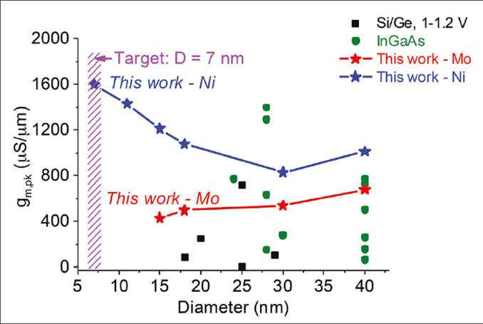
Figure 5. Judged in terms of a peak transconductance at a drain-source voltage of 0.5 V, MIT’s vertical nanowire MOSFET compares well to silicon and germanium variants. The work at MIT is ground-breaking on two fronts: it demonstrates the first sub-10 nm diameter vertical nanowire transistors, and the devices deliver record performance. Note that the labels ‘Ni’ and ‘Mo’ refer to nickel and molybdenum, the metals used in the top contacts of MIT’s vertical nanowire MOSFETs.
We have found that the final annealing step has a profound effect on the electrical characteristics of our devices – especially when they have small diameters. For nanowire MOSFETs with a 7 nm diameter, the absence of annealing leads to a reduction in the on-current by five orders of magnitude, as well as an absence of gate control.
An important figure of merit for benchmarking our transistors against the state-of-the-art is the transconductance. We have undertaken this exercise, considering the peak transconductance of vertical nanowire MOSFETs made from silicon, germanium and III-V materials, and found that our devices produce a very competitive performance, judged against that of silicon and germanium cousins. All devices are rather immature, underlying the potential of the III-V vertical nanowire MOSFET.
It is worth noting that until we announced our recent results, the narrowest silicon vertical nanowire MOSFETs presented in the literature had a diameter of 18 nm, while this figure for InGaAs devices stood at 23 nm. Both these devices are far larger than the target dimension of 7 nm, while our transistors, made with an alcohol-based digital etch, have entered the territory that is relevant for future ultra-scale logic applications.
What is particularly encouraging is that the performance of our nickel-contacted devices continues to improve as their diameter shrinks, with a record transconductance realised for a 7 nm diameter. We attribute this improvement with scaling to a combination of factors, which include volume inversion and a shorter effective channel length, due to enhanced nickel diffusion in narrow devices.
In sharp contrast, devices that are identical, apart from the contact being made of molybdenum rather than nickel, have a performance that degrades as the diameter shrinks (see Figure 5). This stems from increases in the top contact resistance as the contact area is reduced. So great is this problem that if the diameter of the nanowire is reduced to below 15 nm, the device ceases to exhibit transistor characteristics.
We will now build on our success, having demonstrated the smallest vertical nanowire transistor ever made on any kind of material system. Our goals for the future include even higher performance, improved current saturation, reduction of leakage and better reliability. Success in these areas could allow the introduction of III-Vs into logic, and ultimately enable a continuation of the march of Moore’s Law.
Further reading
J. A. del Alamo Nature 479 317 (2011)
H. Riel et al. MRS Bulletin 39 668 (2014)
D. Yakimets et al. IEEE Trans. Electron Devices 62 1433 (2015)
X. Zhao et al. IEDM Tech. Dig. 695 (2013)
X. Zhao et al. IEEE Electron Dev. Lett. 35 521 (2014)
X. Zhao et al. IEDM Tech. Dig. 413 (2017)
W. Lu et al. IEEE Electron Device Lett. 38 548 (2017)
Users of SiC devices are starting to benefit from a dedicated lab that provides new insights into the characteristics of SiC power devices. By Aly Mashaly from Rohm Semiconductor
Power Semiconductors are cropping up everywhere. They are being deployed in electric vehicles, charging station infrastructure, solar and wind power plants, and industrial machinery.
One of the key requirements for every power device is that it complies with energy efficiency requirements. To ensure that this is the case, the devices – either forms of diodes, transistors or thyristors – are tested and validated at an early stage of development. This testing is evolving, due to the introduction of ever higher switching rates and operating voltages.
The cnages in the switching rates and operating voltages are playing into the hands of SiC devices, which have the upper hand over silicon incumbents. But the faster switching speed has a challenging consequence: a need for specialised testing. To meet this requirement, dedicated test setups are needed to deliver the precise results that are desperately wanted by those that will design products with these devices.
At Rohm Semiconductor, a market leader in SiC technology, we are striving to provide our customers with the best possible support. To that end, earlier this year we opened a 300 m2 ‘Power Lab’ for the analysis of power devices and systems. This facility is located in Germany, at our European Headquarters in Willich-Münchheide, which is just outside Düsseldorf.
The primary purpose of our lab is to help our customers realise the benefits of power devices, and to go on and make great products that generate great sales. Our lab can be used to test devices, or systems such as inverters, which may be formed from SiC devices, or a mix of SiC and silicon. One option for our customers is to tell us what testing they require, and trust our engineers to make these measurements – alternatively, they can visit our lab, and use our specialised equipment to carry out the tests themselves.
We know that the engineers that purchase our power devices, or consider doing so, face many challenges. These engineers are under pressure to comply with the current trend of making products that combine higher efficiency with higher power density and higher reliability. Succeeding in this endeavour is not easy, because it brings its own challenges, such as thermal management. Making the engineer’s task even harder, system requirements are getting ever more complex, while the time to complete the project is limited, and it must be accomplished within its financial constraints.
Given this scenario, it’s hardly surprising that many of today’s system engineers are choosing the easiest way to design their circuits. Going into their products are tried-and-tested reference designs, likely to be dominated by silicon chips.
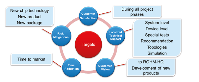
Figure 1. ROHM Semiconductor’s new “Power Lab” aims to provide customers with the best technical support at an application level when using wide bandgap power devices.
To help these engineers make the switch to SiC devices, they need data for these wide bandgap power devices that demonstrates how to use them in applications in the best possible way. Ideally, this data will aid the building of products that are reliable, low in cost, and easy to use.
Makers of SiC power devices, including ourselves, must do more to help every engineer that is considering to use these chips. It is not enough to simply provide a datasheet for each device and system requirements for each power board. Why? Because, for example, the operating points of the final application are not always covered in the datasheets.
Simply adding a few more numbers to the datasheet is not going to address this issue. The reality is that power semiconductors serve in many different application fields, where they operate in many different manners. Depending on the application, there can be different loads, such as DC motors, AC motors and batteries; and there can be different power sources, such as batteries and the grid. The products that are built with these diodes and transistors could be deployed all over the world, so they need to operate over a range of temperatures and humidity levels – and if they are powered by the grid, they need to be compatible with the local power supply.
What the engineers that are building products with power electronics need is technical support. And that is what we can now give them, by making the specific measurements that they need in our new Power Lab. Here, we can test discrete devices under a range of conditions, and also power systems, which may contain a mixture of silicon and SiC components.
The Power Lab project began with a detailed, structured-use case analysis. Throughout the whole project, it was crucial to never lose focus of either the target application or the customers. While making these the priorities, time is taken into account, along with internal and local safety standards.
All these projects benefit from drawing on the great experience of our team, which has many years of experience in power electronic applications and the testing of power devices. The project’s success also results from modern measurement techniques and equipment.
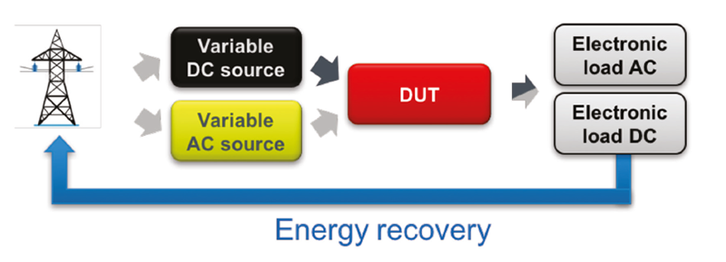
Figure 2. The power test bench feeds energy back into the grid to minimize the energy consumption.
Creating the Power Lab
When we started to plan for the build of our power lab, we had to evaluate the relative importance of many factors. We decided that when we were putting together test benches with state-of-the-art and advanced technologies, emphasis had to be on safety and the quality of the equipment. We also placed a premium on flexibility of usage.
We decided to deploy a flexible, modular design for our test set-ups, because this enables us to provide fast, high-quality support to our customers. What’s more, this gave our Power Lab the capability to be prepared for future products and market trends.
It didn’t take us long to realise that our Power Lab would not be an off-the-shelf product. After specifying the test benches, we had to decide whether we should design the Power Lab ourselves, or hand this task over to an experienced design house. Following careful consideration, we decided on the former. Taking this approach would help to ensure the high quality and reliability of the test benches – and by keeping our know-how in-house, we could ensure that any future modifications would be easier.
After several months of construction, we started using our Power Lab in late 2017 (the official opening followed in 2018). In this purpose-built facility, we can carry out tests on SiC MOSFET transistors, SiC diodes, IGBTs, silicon power MOSFETs and gate drivers at DC voltages of up to 8000 V. These measurements can be carried out in a designated high-voltage room, equipped with several test benches.
The primary purpose of our test benches is the electrical characterization of MOSFETs and IGBTs. For these devices, we can use voltages up to 1500 V to measure switching times and losses, conduction losses and short circuit behaviour. Thanks to the high flexibility of our modular approach, testing is possible on various packages, such as THD, SMD, modules and customer boards.
In our lab, we have converters that can accommodate every configuration of AC and DC input and output, and put devices through their paces under realworld conditions of up to 15 kVA. Our test bench features an AC power supply (grid emulator) and various electronic loads, both in AC and DC form, with maximum voltages under test of 1500 V DC and 400 V AC. In addition, we can provide high-precision measurements of efficiency and losses. And to trim the carbon footprint of our facility, a regenerative function allows us to feed part of the energy that we use back into the grid, reducing our total energy consumption during testing.
The thermal analysis of modules, discrete devices, electronic boards, and even complete power electronics systems can be undertaken on our calorimetric test bench. It features continuous power supplies with a high current level, and a climatic chamber that can range in temperatures from -40 °C to 180 °C and provide humidity levels from 10 percent to 98 percent.
On another test bench, engineers can evaluate the isolation of in-house developed circuits, PCBs and reference designs. For these studies, the power supply enables a programmable output ramp up to 6 kV and 10 mA. For example, this setup can test the clearance and creepage distances of isolated gate driver boards.
Following the opening of our Power Lab, we are strengthening our relationship with our customers, who appreciate our insightful, prompt support at the application level. As well as providing this service, we are starting to undertake our own internal projects. Our aim with these test boards is to put power devices through their paces at the system level. Evaluations will be from a customer perspective. The results of these efforts will soon be published, in the form of application notes and reference designs.
