A technology magazine saying that it is ‘looking to the future’ is no surprise. Technology is the future; every edition looks that direction. Our focus is always about pushing boundaries while avoiding setbacks and detours. The thing is, getting to ‘the future’ for silicon device manufacturers used to be a comparatively simple exercise in scaling. How the times have changed!
For the silicon semiconductor industry, delivering greater performance at lower costs used to rely upon traditional geometric scaling principles even if the details involved many twists and turns. But we knew the way. Getting from 48/45nm features to 28nm was straightforward: decrease transistor element sizes ‘x’ amount using processes well established at the last node, plus some innovations here and there. While this observation dramatically oversimplifies complex lithographic feats du jour, new materials exactness and myriad other complications, transitioning meant using know technologies to deliver what customers wanted to buy: greater densities, faster speeds, superior efficiencies and overall greater performance.
Today, all bets are off when it comes to tried and true approaches to achieving 7/5nm device geometries. Getting to 14nm and then 10nm was challenging enough. That journey took new approaches and increasingly complex photo lithographic feats that today involve 3D structures such a FinFETs, double- and quadruple multi pattern immersion lithography, wafer bonding and obsessively demanding material purity standards.
For years the industry’s largest device fabs including Intel, Samsung, TSMC, Globalfoundries and others pinned future hopes to the development and roll-out of extreme ultraviolet (EUV) lithography. But enabling EUV to meet the demands of highly-demanding customers has dragged on. For years. Not enough power; problematic pellicles; and so on. Delays were followed by more delays; major foundries postponed their switch-over. And by the way, did we mention the current price for a single EUV tool? About USD $100 million. Ouch...
In this Silicon Semiconductor we explore how different companies are looking to the future and seeing it not as a destination with one road, but as having many different means to arrive at different places. On page 22 we explore solutions for many device types and alternative technologies beyond CMOS scaling. Our cover feature on page 16 looks at the work of Brewer Science and two product lines supporting temporary wafer bonding (TWB) and their breakthrough work in directed self-assembly (DSA).
Join us in the future. There are many roads, and a ticket doesn’t require a billion-euro fab.
Globalfoundries has announced that its 180 nm Ultra High Voltage (180UHV) technology platform has entered volume production for a range of client applications, including AC-DC controllers for industrial power supplies, wireless charging, solid state and LED lighting, as well as AC adapters for consumer electronics and smartphones.
The increasing demand for highly costeffective systems requires integrated circuits (ICs) that achieve significant area savings while reducing bill-ofmaterials (BOM) and printed circuit board (PCB) footprint by integrating discrete components onto the same die. GF’s 180UHV platform features a 3.3 V LV CMOS baseline, with options for HV18, HV 30 and 700V UHV, that delivers significant area savings for both digital and analog circuit blocks, compared to the traditional 5V bipolar CMOS DMOS (BCD) technologies.
“GF’s leadership in providing high voltage solutions makes the company a perfect strategic partner for On-Bright’s power supply technologies,” said Julian Chen, CEO of On-Bright, the leading market player in AC-DC switch mode power supply products. “GF’s new 180UHV process integrates UHV components into the same IC with 180 nm digital and analog by incorporating On-Bright know-how in the design. The technology has reduced On-Bright’s switched-mode power supply cost and footprint to give our AC-DC switch mode power supply products additional system-level benefits.”
As part of a modular platform based on the company’s 180 nm process node, GF’s 180UHV process technology delivers a 10x increase in digital density compared to previous generations for integrated AC-DC conversion. For AC-DC conversion, the platform integrates high voltage transistors with precision analog and passive devices to control high input and output voltages of AC-DC SMPS circuits. The process is qualified up to 150°C to accommodate the high ambient temperatures of power supply and LED lighting products.
“GF continues to expand its UHV portfolio to provide competitive technology capabilities and manufacturing excellence that will enable our customers to play a critical role in bringing a new generation of highly integrated devices to real-world environments,” said Dr. Bami Bastani, senior vice president of business units at GF. “Our 180UHV is an ideal technology for customers that are looking to develop the highest-performing solutions for a new generation of integrated digital, analog and high voltage applications.”
As a part of the company’s analog and power platform, GF provides various types of HV, BCD, and UHV technologies, allowing customers to integrate power and high voltage transistors across a wide range of voltages, from 5 V to 700 V, to meet the diverse needs of low and high power applications. GF has a successful track record in manufacturing analog and power solutions in both its 200 mm and 300 mm production lines in Singapore.
Orbotech a global supplier of yield-enhancing and process-enabling solutions for the manufacture of electronics products, and A*STAR’s Institute of Microelectronics (IME), have announced a joint lab agreement confirming Orbotech as a partner in IME’s FOWLP joint lab and as a member of the IME FOWLP development line consortium.
Orbotech’s Emerald UV Laser Drilling solution is one of the key processes available in the FOWLP joint lab development line. The Emerald delivers advanced UV drilling performance for today’s most challenging IC substrate and assembly applications, including 3D packages, stacking and package on package.
The FOWLP development line at IME’s facilities at Singapore Science Park II, and its new facilities at Fusionopolis Two, will allow IME and its partners to develop technologies that will serve a wide range of markets including consumer electronics, healthcare and automotive.
“Orbotech is honored to be part of IME’s FOWLP development joint lab and FOWLP development line consortium,” said Dr. Abraham Gross, Corporate Executive Vice President, Chief Technology Officer and Head of Innovation of Orbotech. “This collaboration builds on the long-term relationship that IME has with Orbotech’s SPTS Technologies, a leading supplier of advanced packaging solutions. We are always pleased to cooperate with technology and process innovation initiatives that push the electronics packaging industry forward and enable solutions for complex challenges. The Emerald UV Laser Drilling system is just one of the building blocks that we, at Orbotech, provide to enhance the quality and efficiency of the production process for 3D IC and other complex high density packaging structures.”
Amicra Microtechnologies, a vendor of back-end processing equipment for advanced packaging applications and silicon photonics assembly, is entering a new era of growth and market capitalization by becoming a part of ASM Pacific Technology Ltd. (ASMPT). Effective April 2018, the company was renamed ASM AMICRA Microtechnologies GmbH. The wellknown AMICRA management team, consisting of Dr. Johann Weinhaendler, Rudolf Kaiser and Horst Lapsien, remains in place.
The acquisition of 100% of the shares of AMICRA Microtechnologies GmbH by Singapore-based ASM Pacific Technology Ltd. (ASMPT) will considerably expand and strengthen AMICRA’s strategic position. ASMPT, as an innovative and quality-driven strategic investor in the electronics manufacturing industry having a welldeveloped distribution network in Asia, complements AMICRA’s technology position and worldwide business activities very well.
The transaction will especially serve the fast growing silicon photonics assembly equipment market but also the general high-precision flip-chip and die bonding markets.
ASMPT, headquartered in Singapore and listed on the Hong Kong Stock Exchange, is the world’s largest backend semiconductor equipment supplier and SMT solutions provider. ASM AMICRA Microtechnologies GmbH will be integrated into ASMPT’s back-end equipment segment. AMICRA’s corporate structure and global organization will remain in place, as well its long-time proven management team.
AMICRA started out in 2001 with five employees. In the mean time, it has developed into an internationally known vendor and leading supplier of highprecision die bonders for the advanced packaging and photonics assembly market.
AMICRA now employs 130 at its headquarters in Regensburg, Germany, and in twelve sales and tech support offices around the world. AMICRA products will now constitute an important growth factor for the global leader in back-end equipment.
ASMPT’s commanding market position is based on its continued technological innovation, its foresight in investing ahead of the curve, commitment to quality, and strong value-adding services to customers.
ASMPT currently invests about ten percent of its revenues in R&D. This makes it an ideal partner for an innovation and technology leader in photonics and optical device packaging such as AMICRA.
Following its successful penetration of the worldwide markets for high-precision die-attach equipment, especially in the rapidly growing silicon photonics assembly segment, AMICRA saw a perfect opportunity to merge with a strong strategic partner to better support its growing international customers base.
With ASMPT’s economic scale and well established supply chains and customer support capabilities, this will allow AMICRA to take the next step in the development of its business.
Dr Johann Weinhaendler, a member of the AMICRA executive management team, stated: “We are delighted to work with ASMPT. The expanded operational base offered by ASMPT is very important to us. We will continue to be a reliable partner to our existing and new customers focused on their specific needs and requirements. We will continue to offer excellent support, as well as innovative solutions.
“AMICRA’s sub-micron high-accuracy die bonder product is complementary to the ASMPT group’s existing portfolio and the AMICRAs leading position in the photonics assembly market, gives a high growth potential for AMICRA and ASMPT. We are confident that this joining of forces will further strengthen our growth opportunities and deliver even higher added value to our common customers.”
Veeco Instruments has announced financial results for its first quarter ended March 31, 2018. Highlights include: revenues of $158.6 million, compared with $94.5 million in the same period last year; GAAP net loss of $15.8 million, or $0.34 loss per share; and non-GAAP net income of $9.2 million, or $0.20 per diluted share
“2018 is off to a great start with strong sequential and year-over-year revenue growth. Our Non-GAAP gross margin, operating income, net income and EPS all exceeded our guided ranges,” commented John R. Peeler, chairman and CEO. “Sales growth in the first quarter was driven primarily by shipments of our lithography systems into the advanced packaging market, and shipments of MOCVD systems for LED applications.
“As we work towards our goal of being a more diversified company, we are pleased to see orders grow in the Front-End Semi and Advanced Packaging, MEMS & RF Filter markets,” continued Peeler. “Our Ultratech integration is also proceeding well and we remain encouraged with Veeco’s growth prospects ahead.”
The following guidance is provided for Veeco’s second quarter 2018: Revenue is expected in the range of $145 million to $170 million; non-GAAP operating income is expected in the range of $2 million to $11 million; GAAP earnings (loss) per share are expected in the range of ($0.45) to ($0.26); non-GAAP earnings (loss) per share are expected in the range of $0.01 to $0.20.
According to “Global Semiconductor Equipment: Markets, Market Shares, Market Forecasts,” the front-end equipment market, which grew 18.4% in 2014 based on revenues converted to dollars, the 2015 market decreased 2.4%. A number of technical and operational trends within the semiconductor manufacturing industry are strengthening the need for more effective advanced equipment solutions.
These trends include: Development of Smaller Semiconductor Features. The development of smaller features, now as small as 20nm in production and 10nm in R&D, enables semiconductor manufacturers to produce larger numbers of circuits per wafer and to achieve higher circuit performance.
Transition to 3D device structures. Foundries are adopting 3D FinFET transistors starting at 14/16 nm technology nodes to get improved performance and use less power in 1x technology nodes. Memory makers will move to 3D NAND and vertical structures for next generation NAND technology
Transition to 3D Integration Technology. Three-dimensional (3D) integration of active devices, directly connecting multiple IC chips, offers many benefits, including power efficiency, performance enhancements, significant product miniaturization, and cost reduction. It provides an additional way to extend Moore’s law beyond spending ever increasing efforts to shrink feature sizes. A critical element in enabling 3D integration is the Through-Silicon Via (TSV); TSV provides the high-bandwidth interconnection between stacked chips. The TSV process is beginning to enter production. In the case of TSV, since multiple chips are connected, the process must achieve and maintain very high yield levels in order to be economically viable.
Shortening of Technology Life Cycles. The technology life cycle of integrated circuits continues to shorten as semiconductor manufacturers strive to adopt new processes that allow a faster transition to smaller, faster and more complex devices. In the past, the technology life cycle was approximately three years; it is now only two years.
New materials. Copper metal layers continue to be the key material for the back end of line for advanced integrated circuits in order to increase performance and reduce the cost of integrated circuits. The Industry is continuously searching directions to reduce the effective K of the low K materials and to reduce the barrier thickness and material types.
These changes require new processing and metrology equipment and thus represents challenging developments for the semiconductor manufacturing industry. In addition, in order to overcome limitations in the continued shrink of transistor dimensions, leading edge integrated circuit manufacturers are introducing new materials in the transistor gate stack. The adoption of high-k dielectrics is a key element for gate control in the most advanced technology nodes of 28nm, 20nm and 14nm currently in production, while R&D work to implement the next gate control material being done with III-IV materials. These new materials, combined with metal layers, require new processing and metrology equipment and thus represent a challenging development for the semiconductor manufacturing industry. Increasing use of multi patterning lithography. The continuous need for scaling to meet reduced transistor costs combined with delays in EUV lithography is pushing the industry to develop alternative lithography techniques such as multi patterning, DSA and E-Beam. These alternative technologies are increasing the Etch and CMP process steps and thus increasing the process control and metrology steps in these areas accordingly.
Increase in Foundry Manufacturing. Because of the rising investment needed for semiconductor process development and production as well as the proliferation of different types of semiconductors, semiconductor manufacturing is increasingly being outsourced to large semiconductor contract manufacturers, or foundries. A foundry typically runs several different processes and makes hundreds to thousands of different semiconductor product types in one facility, making the maintenance of a constant high production yield and overall equipment efficiency more difficult to achieve. This trend of shifting to foundries for manufacturing needs has progressed even further during recent years.
This report forecasts for all WFE equipment 2012-2018. Market shares for 2015. Profiles of all equipment vendors.
GLOBALFOUNDRIES has announced that its 45nm RF SOI (45RFSOI) technology platform has been qualified and is ready for volume production. Several customers are currently engaged for this advanced RF SOI process, which is targeted for 5G millimeter-wave (mmWave) front-end module (FEM) applications, including smartphones and next-generation mmWave beamforming systems in future base stations.
As next-generation systems move to frequencies above 24GHz, higher performance RF silicon solutions are required to exploit the large available bandwidth in the mmWave spectrum. GF’s 45RFSOI platform is optimized for beam forming FEMs, with features that improve RF performance through combining high-frequency transistors, high-resistivity silicon-on-insulator (SOI) substrates and ultra-thick copper wiring.
Moreover, the SOI technology enables easy integration of power amplifiers, switches, LNAs, phase shifters, up/down converters and VCO/PLLs that lowers cost, size and power compared to competing technologies targeting tomorrow’s multi-gigabit-per-second communication systems, including internet broadband satellite, smartphones and 5G infrastructure.
“GF’s leadership in RF SOI solutions makes the company a perfect strategic partner for Peregrine’s next generation of RF SOI technologies,” said Jim Cable, Chairman and CTO of Peregrine Semiconductor. “It enables us to create RF solutions that provide our customers with new levels of product performance, reliability and scalability, and it allows us to push the envelope of integrated RF front-end innovation for evolving mmWave applications and emerging 5G markets.”
“To bring 5G into the future, mmWave innovations are needed for allocating more bandwidth to deliver faster, higher-quality video, and multimedia content and services,” Bob Donahue, CEO of Anokiwave. “GF’s RF SOI technology leadership and 45RFSOI platform enables Anokiwave to develop differentiated solutions designed to operate between the mmWave and sub-6GHz frequency band for high-speed wireless communications and networks.”
“GF continues to expand its RF capabilities and portfolio to provide competitive RF SOI advantages and manufacturing excellence that will enable our customers to play a critical role in bringing 5G devices and networks to real-world environments,” said Bami Bastani, senior vice president of the RF Business Unit at GF. “Our 45RFSOI is an ideal technology for customers that are looking to deliver the highest- performing mmWave solutions that will handle demanding performance requirements in next-generation mobile and 5G communications.”
GF’s RF SOI solutions are part of the company’s vision to develop and deliver the next wave of 5G technology aimed at enabling connected intelligence for next generation devices, networks and wired/wireless systems. GF has a successful track record in manufacturing RF SOI solutions at its 300mm production line in East Fishkill, N.Y. Customers can now start optimizing their chip designs to develop differentiated solutions for high performance in the RF front end for 5G and mmWave applications.
Infineon Technologies AG reported its results for the first quarter of the 2018 fiscal year (period ended 31 December 2017).
“Infineon has made a strong start to the new fiscal year, stated Dr. Reinhard Ploss, CEO of Infineon. Earnings and margin were better than forecast – despite the expected slight seasonal dip in revenues. The market for electro-mobility continues to drive growth. Infineon offers solutions for the entire range of drivetrain systems from hybrid to pure electric vehicles.
Moreover, we continue to benefit from excellent market conditions, which are driving high demand for power components used in applications across the board, such as solar power plants, especially in China, and for data centres. Operationally we are fully on track. We could still defy the headwind from the weaker US$ in the fiscal first quarter. Adjusted for the depreciation of the US$ from 1.15 to 1.25, our revenue momentum is unchanged, in terms of the Segment Result Margin even slightly better. However, we are unable to compensate a further depreciation of the US$ by another 8 percentage points, which negatively affects more than half of our revenues. As such, we currency adjusted our outlook accordingly.”
Compared to the preceding quarter, revenue declined by 2 percent to €1,775 million in the first quarter of the 2018 fiscal year. Revenue in the previous quarter had amounted to €1,820 million. Compared to the first quarter of the 2017 fiscal year, revenues increased by 8 percent. The Industrial Power Control (IPC), Power Management & Multimarket (PMM) and Chip Card & Security (CCS) segments all reported seasonal decreases, whereas the Automotive segment (ATV) recorded seasonally atypical revenue growth in line with expectations.
The gross margin in the first quarter came in at 36.4 percent, compared to 37.5 percent in the previous quarter. These figures include acquisition-related depreciation and amortization as well as other expenses attributable to the International Rectifier acquisition totaling €17 million. The adjusted gross margin came in at 37.4 percent, compared with 38.6 percent in the preceding quarter. The first-quarter Segment Result amounted to €283 million, compared to €328 million in the fourth quarter of the previous fiscal year, with the Segment Result Margin declining from 18.0 percent to 15.9 percent.
The first-quarter non-segment result improved to a net loss of €35 million, compared to the net loss of €56 million reported for the preceding quarter. Of the first-quarter figure, €18 million related to the cost of goods sold, €16 million to selling, general and administrative expenses and €1 million to research and development expenses. The non-segment result for the first quarter includes €30 million of depreciation and amortization arising in conjunction with the purchase price allocation and other expenses for post-merger integration measures relating to International Rectifier.
Operating income for the first quarter totalled €248 million, compared to €272 million in the preceding quarter. Income from continuing operations for the three-month period improved to €206 million. The corresponding figure for the previous quarter had been €177 million. Income from discontinued operations remained stable at a negative amount of €1 million. Net income increased from €176 million to €205 million quarter-on-quarter. The firstquarter income tax expense amounted to €28 million, significantly lower than the tax expense of €84 million reported for the fourth quarter.

Earnings per share improved quarter-onquarter from €0.16 to €0.18 (basic and diluted in each case). Adjusted earnings per share1 (diluted) amounted to €0.20, compared to €0.22 in the fourth quarter. For the purpose of calculating adjusted earnings per share (diluted), a number of items are eliminated, most notably acquisition-related depreciation/amortization and other expenses (net of tax) as well as valuation allowances on deferred tax assets.
Investments – which Infineon defines as the sum of purchases of property, plant and equipment, purchases of intangible assets and capitalized development costs – amounted to €293 million in the first quarter of the 2018 fiscal year, compared to €370 million in the preceding three-month period. Depreciation and amortization remained almost unchanged at €204 million, compared to the previous quarter’s €205 million.
First-quarter free cash flow2 from continuing operations was a negative amount of €135 million, compared to a positive amount of €249 million one quarter earlier. Net cash provided by operating activities from continuing operations amounted to €158 million, compared to the previous quarter’s €616 million.
The gross cash position at the end of the first quarter of the 2018 fiscal year amounted to €2,312 million, compared to €2,452 million at 30 September 2017. The net cash position amounted to €503 million, compared to €618 million three months earlier.
Provisions relating to Qimonda decreased from €33 million at 30 September 2017 to €32 million at 31 December 2017. These provisions are recognized for legal costs in conjunction with the defense against claims made by the Qimonda insolvency administrator and for residual liabilities related to Qimonda Dresden GmbH & Co. OHG. In the second quarter of the 2018 fiscal year, Infineon expects a quarter-onquarter revenue increase of 4 percent (plus or minus 2 percentage points).
The forecast is based on an assumed exchange rate of US$1.25 to the euro for the remainder of the quarter. At the midpoint of revenue guidance, the Segment Result Margin is expected to come in at 16 percent.
Amphion Semiconductor, a video codec silicon IP provider, has announced the release of the latest version of its successful, ‘Malone’ video decoder IP core optimized for SoC implementation.
Architectural optimizations have enabled Amphion’s video SoC experts to realize further reductions in the size of the core area while maintaining the performance necessary to support the latest resolution and frame rate demands. In addition to supporting all legacy formats, the CS8141 version of the Malone video decoder supports the very popular HEVC and VP9 formats in a single core. VP9 is supported for Profile 0 and Profile 2 at Level 5.1, giving up to 12-bit color depth and covering resolutions and frame rates up to 4Kp60.
Furthermore, for applications that require it, the core can be configured for frame rates of up to 120fps and image resolutions of up to 8K. The Malone family of advanced video decode cores have been licensed by many semiconductor and SoC companies. Due to the modular nature of the Malone architecture, customers can select which formats they need to support and at what resolution and frame rate and Amphion will configure a highly optimized solution which is minimal in both silicon area and power consumption for their application.
Shaped like a spine, new design enables remarkable flexibility, high energy density, and stable voltage no matter how it is flexed or twisted.
The rapid development of flexible and wearable electronics is giving rise to an exciting range of applications, from smart watches and flexible displays—such as smart phones, tablets, and TV—to smart fabrics, smart glass, transdermal patches, sensors, and more. With this rise, demand has increased for high-performance flexible batteries. Up to now, however, researchers have had difficulty obtaining both good flexibility and high energy density concurrently in lithium-ion batteries.
A team led by Yuan Yang, assistant professor of materials science and engineering in the department of applied physics and mathematics at Columbia Engineering, has developed a prototype that addresses this challenge: a Li-ion battery shaped like the human spine that allows remarkable flexibility, high energy density, and stable voltage no matter how it is flexed or twisted. The study is published today in Advanced Materials.
“The energy density of our prototype is one of the highest reported so far,” says Yang. “We’ve developed a simple and scalable approach to fabricate a flexible spine-like lithium ion battery that has excellent electrochemical and mechanical properties. Our design is a very promising candidate as the firstgeneration, flexible, commercial lithium-ion battery. We are now optimizing the design and improving its performance.”

Yang, whose group explores the composition and structure of battery materials to realize high performance, was inspired by the suppleness of the spine while doing sit-ups in the gym. The human spine is highly flexible and distortable as well as mechanically robust, as it contains soft marrow components that interconnect hard vertebra parts.
Yang used the spine model to design a battery with a similar structure. His prototype has a thick, rigid segment that stores energy by winding the electrodes (“vertebrae”) around a thin, flexible part (“marrow”) that connects the vertebra-like stacks of electrodes together. His design provides excellent flexibility for the whole battery.
“As the volume of the rigid electrode part is significantly larger than the flexible interconnection, the energy density of such a flexible battery can be greater than 85 percent of a battery in standard commercial packaging,” Yang explains. “Because of the high proportion of the active materials in the whole structure, our spine-like battery shows very high energy density—higher than any other reports we are aware of. The battery also successfully survived a harsh dynamic mechanical load test because of our rational bio-inspired design.”
Yang’s team cut the conventional anode/separator/cathode/separator stacks into long strips with multiple “branches” extending out 90 degrees from the “backbone.” Then they wrapped each branch around the backbone to form thick stacks for storing energy, like vertebrae in a spine. With this integrated design, the battery’s energy density is limited only by the longitudinal percentage of vertebra-like stacks compared to the whole length of the device, which can easily reach over 90 percent.

The battery shows stable capacity upon cycling, as well as a stable voltage profile no matter how it is flexed or twisted. After cycling, the team disassembled the battery to examine the morphology change of electrode materials. They found that the positive electrode was intact with no obvious cracking or peeling from the aluminum foil, confirming the mechanical stability of their design.
To further illustrate the flexibility of their design, the researchers continuously flexed or twisted the battery during discharge, finding that neither bending nor twisting interrupted the voltage curve. Even when the cell was continuously flexed and twisted during the whole discharge, the voltage profile remained. The battery in the flexed state was also cycled at higher current densities, and the capacity retention was quite high (84 percent at 3C, the charge in 1/3 of an hour). The battery also survived a continuous dynamic mechanical load test, rarely reported in earlier studies. “Our spine-like design is much more mechanically robust than are conventional designs,” Yang says. “We anticipate that our bio-inspired, scalable method to fabricate flexible Li-ion batteries could greatly advance the commercialization of flexible devices.”
About the Study
The study is titled “Bio-inspired, spine-like flexible rechargeable lithium-ion batteries with high energy density.”
The authors declare no financial or other conflicts of interest.
Authors
Guoyu Qian, Bin Zhu, Haowei Zhai, Nathan Joseph Fritz, Qian Cheng, Mingqiang Ning, Boyu Qie, and Yuan Yang (Materials Science and Engineering Program, Department of Applied Physics and Applied Mathematics, Columbia Engineering); Arvind Srinivasan (Department of Mechanical Engineering, Columbia Engineering); Xiangbiao Liao and Xi Chen (Department of Earth and Environmental Engineering, Columbia Engineering);
Yi Li (Visual Communication Department, School of the Art Institute of Chicago); Songliu Yuan (School of Physics, Huazhong University of Science and Technology); Jia Zhu, (College of Engineering and Applied Science, Nanjing University ).
The study was supported by startup funding from Columbia University, and the NSF MRSEC program through Columbia in the Center for Precision Assembly of Superstratic and Superatomic Solids (DMR-1420634) and sponsored by the China Scholarship Council (CSC) graduate scholarship.
A team led by Princeton University researchers has created an essential component for making quantum computers from an everyday material, silicon. The researchers demonstrated the ability to control the behavior of two silicon-based quantum bits, or qubits, paving the way for making complex, multi-qubit devices using technology that is less expensive and easier to manufacture than other approaches. Photo by David Zajac.
In a major step toward making a quantum computer using everyday materials, a team led by researchers at Princeton University has constructed a key piece of silicon hardware capable of controlling quantum behaviour between two electrons with extremely high precision. The study was published in December 2017 in the journal Science.
The team constructed a gate that controls interactions between the electrons in a way that allows them to act as the quantum bits of information, or qubits, necessary for quantum computing. The demonstration of this nearly error-free, two-qubit gate is an important early step in building a more complex quantum computing device from silicon, the same material used in conventional computers and smartphones. “We knew we needed to get this experiment to work if silicon-based technology was going to have a future in terms of scaling up and building a quantum computer,” said Jason Petta, a professor of physics at Princeton University. “The creation of this highfidelity two-qubit gate opens the door to larger scale experiments.”
Copyright: David Zajac, Princeton University
Silicon-based devices are likely to be less expensive and easier to manufacture than other technologies for achieving a quantum computer. Although other research groups and companies have announced quantum devices containing 50 or more qubits, those systems require exotic materials such as superconductors or charged atoms held in place by lasers.
Quantum computers can solve problems that are inaccessible with conventional computers. The devices may be able to factor extremely large numbers or find the optimal solutions for complex problems. They could also help researchers understand the physical properties of extremely small particles such as atoms and molecules, leading to advances in areas such as materials science and drug discovery.
The two-qubit silicon-based gate consists of two electrons (blue balls with arrows) in a layer of silicon (Si). By applying voltages through aluminum oxide (Al2O3)wires (red and green), the researchers trapped the electrons and coaxed quantum behaviors that transform their spin properties into quantum bits of information, or qubits. The image on the left shows a scanning electron micrograph of the device, which is about 200 nanometers (nm) across. The image on the right is a diagram of the device from the side. Image credit Science/AAAS.
Building a quantum computer requires researchers to create qubits and couple them to each other with high fidelity. Silicon-based quantum devices use a quantum property of electrons called “spin” to encode information. The spin can point either up or down in a manner analogous to the north and south poles of a magnet. In contrast, conventional computers work by manipulating the electron’s negative charge. Achieving a high-performance, spin-based quantum device has been hampered by the fragility of spin states — they readily flip from up to down or vice versa unless they can be isolated in a very pure environment. By building the silicon quantum devices in Princeton’s Quantum Device Nanofabrication Laboratory, the researchers were able to keep the spins coherent — that is, in their quantum states — for relatively long periods of time.
To construct the two-qubit gate, the researchers layered tiny aluminum wires onto a highly ordered silicon crystal. The wires deliver voltages that trap two single electrons, separated by an energy barrier, in a well-like structure called a double quantum dot.
By temporarily lowering the energy barrier, the researchers allow the electrons to share quantum information, creating a special quantum state called entanglement. These trapped and entangled electrons are now ready for use as qubits, which are like conventional computer bits but with superpowers: while a conventional bit can represent a zero or a 1, each qubit can be simultaneously a zero and a 1, greatly expanding the number of possible permutations that can be compared instantaneously. “The challenge is that it’s very difficult to build artificial structures small enough to trap and control single electrons without destroying their long storage times,” said David Zajac, a graduate student in physics at Princeton and first-author on the study. “This is the first demonstration of entanglement between two electron spins in silicon, a material known for providing one of the cleanest environments for electron spin states.”
The researchers demonstrated that they can use the first qubit to control the second qubit, signifying that the structure functioned as a controlled NOT (CNOT) gate, which is the quantum version of a commonly used computer circuit component. The researchers control the behavior of the first qubit by applying a magnetic field. The gate produces a result based on the state of the first qubit: If the first spin is pointed up, then the second qubit’s spin will flip, but if the first spin is down, the second one will not flip.
Copyright: David Zajac, Princeton University
“The gate is basically saying it is only going to do something to one particle if the other particle is in a certain configuration,” Petta said. “What happens to one particle depends on the other particle.” The researchers showed that they can maintain the electron spins in their quantum states with a fidelity exceeding 99 percent and that the gate works reliably to flip the spin of the second qubit about 75 percent of the time. The technology has the potential to scale to more qubits with even lower error rates, according to the researchers.
“This work stands out in a worldwide race to demonstrate the CNOT gate, a fundamental building block for quantum computation, in silicon-based qubits,” said HongWen Jiang, a professor of physics and astronomy at the University of California-Los Angeles. “The error rate for the two-qubit operation is unambiguously benchmarked. It is particularly impressive that this extraordinarily difficult experiment, which requires a sophisticated device fabrication and an exquisite control of quantum states, is done in a university lab consisting of only a few researchers.” Additional researchers at Princeton are graduate student Felix Borjans and associate research scholar Anthony Sigillito. The team included input on the theory aspects of the work by Jacob Taylor, a professor at the Joint Quantum Institute and Joint Center for Quantum Information and Computer Science at the National Institute of Standards and Technology and the University of Maryland, and Maximilian Russ and Guido Burkard at the University of Konstanz in Germany.
Research was sponsored by U.S. Army Research Office grant W911NF-15-1-0149, the Gordon and Betty Moore Foundation’s EPiQS Initiative through grant GBMF4535, and National Science Foundation grant DMR-1409556. Devices were fabricated in the Princeton University Quantum Device Nanofabrication Laboratory.
The study, “Resonantly driven CNOT gate for electron spins,” by David M. Zajac, Anthony J. Sigillito, Maximilian Russ, Felix Borjans, Jacob M. Taylor, Guido Burkard and Jason R. Petta was published online in the journal Science on Dec. 7, 2017.
New generations of high power/high performance semiconductors are enabling more robust electronic systems. But higher power densities, new materials and demanding process requirements have challenged existing bonding techniques. ATV Technologie has a new solution that reduces pressure, strengthens bonds and improves throughput. By Mark Andrews technical editor Silicon Semiconductor.
High density semiconductor die that increase a component’s power handling capabilities while saving space and increasing efficiency are key to the functionality of electric vehicles (EVs) and renewable energy systems along with aviation and aerospace power assemblies.
Designers and manufacturers often face a dilemma: how to create void-free, permanent bonds between die, thermal spreaders and other module components without dramatically slowing production, adding costs or crushing yield. The researchers and designers at ATV Technologie GmbH (Vaterstetten, Germany) are well positioned to understand the complexities of bonding processes. They have met the challenges of creating bonds effectively, with high repeatability and sufficient throughput to satisfy the needs of environments that vary greatly such as those found at research institutes, across prototype lines and volume manufacturing.
In order to create void-free bonds, existing systems such as silver (Ag) sintering often utilize pressure as great as 15-40 MPa. While these systems deliver good bonds, the high amount of relative pressure often creates situations where breakage is more likely, adversely affecting yield and long-term reliability. Existing systems also frequently do not handle devices with varying height profiles in the same batch, or require special, complex tooling to accommodate such needs. High temperature sintering typically does not support bonding temperature-sensitive semiconductor components that might warp, crack or lose electrical viability due to intense pressure or heat.
Figure 1: Process stages of Transient Liquid Phase Bonding (TLPB)
Wide bandgap technologies including gallium nitride (GaN) and silicon carbide (SiC) are moving rapidly into high volume manufacturing (HVM) since issues that limited widespread use of these high power technologies are largely being overcome by industry-wide efforts. The development of ATV’s new system was largely driven by the demand for highly reliable insulated-gate bipolar transistor (IGBT) power modules in EVs; however, any similar need could be served. The company explained that die bonding of power LEDs has great potential, as well as applications such as piezoelectric devices for energy harvesting, TC coolers and RF power modules demanding new packaging solutions.
Automotive applications are particularly challenging since operating environments are many degrees centigrade above that of consumer electronics, and zero defects is the quality target for such devices that have to last at least 10 years in-service.
While manufacturers are regularly extending GaN device lifetimes and yield improvements have made the technology completely viable across market sectors, packaging requirements can present vexing issues. As ATV Technical Director, Dr. Ventzeslav Rangelov remarked, conventional lead-free reflow soldering has reached its limits in most applications that are becoming more critical to the future of high power semiconductor markets.
“For assemblies that need to operate at or above 165°C, new die attach techniques including silver sintering and transient liquid phase bonding (TLPB) have been developed,” he noted. “The latest system that ATV developed with the Technical University of Berlin and the Fraunhofer Institute can solve vexing issues that can hold back needed products from entering production. It can help researchers explore new device types and even higher levels of power without the drawbacks of other approaches.”
ATV’s new approach to device bonding processes remedies the drawbacks of other techniques, such as pressure assisted Ag sintering. While silver is prized for its high melting point and excellent thermal conductivity, standard sintering processes have issues related to their requirement for high applied pressure. In standard reflow soldering there is also excess material present when peak temperatures are reached, resulting in certain amounts of self-realignment driven by capillary action. This misalignment can in particular cases affect yield and function of the assembly. With Ag sintering, mechanical pressure is exerted to enable diffusive joining mechanisms. But to be effective the pressure can be as great as 40 MPa, often resulting in some warpage, cracks in device structures or outright device breaks. When pressure combines with high levels of heat (250°C or greater) there can be a loss of surface contact across the device, often in unpredictable directions with negative performance consequences.
While pressure-assisted silver sintering processes have been refined and have widely entered volume manufacturing, a new approach that addresses shortcomings is now available, Rangelov noted.
“In TLPB, a thin layer of lower-melting metal such as tin or indium is placed between the two higher melting base metals, such as silver, gold or copper,” he explained. “During thermal bonding, the solder interlayer melts and wets the base metal surfaces—the interlayer dissolves an amount of the base metal, forming new intermetallic phases. This process leads to isothermal solidifications that create a joint layer with significantly higher melting temperature than the initial solder interlayer.” (See Figure 1)
“Once the intermetallic components are formed during bonding, they cannot be melted anymore at the original process temperature, which is close to the melting point of the interlayer metal, such as tin or indium. This is because of the change of the material composition during TLPB. It is defined by the material properties and their proportion and not by the process itself. The change of material composition is due to diffusion and promotes the isothermal solidification. This is also the main difference in our process compared to conventional reflow soldering where the composition of the solder material remains quite the same,” he explained.
Figure 2: Schematic drawing of ATV’s new bonding oven
Conventional Ag sintering and TLPB both require some levels of mechanical pressure under heat, but TLPB only requires enough pressure to hold the surfaces being bonded together to the point that a bond can form without misalignment.
Thermal load requirements are also far less. ATV has also eliminated the need for complex additional mechanical pressure tooling to cope with whole assemblies that exhibit complex topographies. ATV’s system has been tested with form factors varying from 0.5mm to 3.0mm—all in the same batch.
Despite the sizeable variations in height profiles, bonding was void free with high yield. In most competing systems, the ability to compensate for height variations drives up complexity and costs of tooling, Rangelov noted. Also, the fact that bare metals are involved in processing requires gas-tight chambers with controlled inert or reducing process atmosphere. ATV’s approach handles these needs while others do not.
“The main benefit is that customers do not need expensive height compensating tooling, which is individually designed for any different layout. This lowers the costs and has a positive effect on yield. In the bonding system, whole electronic assemblies with complex topographies can be processed. Passive and active devices as well as clips can be bonded in one process run. This can give more flexibility in the packaging process flow.”
“Our bonding system techniques can also be beneficial in conventional reflow soldering, when parts have to be kept in position precisely during the liquidity phase. This is not always possible with alignment masks (other systems require), especially when parts are very small, or different CTE might be an issue,” he remarked.
ATV developed a system that combines established equipment for vacuum reflow soldering with a dedicated press unit (see Figure 2). Their process supports semiconductor die or other packaged components that are aligned and placed on a substrate for DCB (direct copper bonding). It also supports wafers that are either flipped or face up utilizing industry standard handling equipment. For tacking operations, Rangelov said a liquid adhesive, ultrasonic energy or thermo-compression can be used, offering flexibility to suit existing practices, whether in the lab or fab.
ATV Technical Director, Dr. Ventzeslav Rangelov
High throughput can be achieved at the highest alignment accuracy, he added. In repeated tests of their new system, Rangelov noted that ATV utilized subjects that varied in thickness, achieving excellent void-free results. This was also achieved with pressures of only 0.5 MPa (or less), substantially reducing the possibility of warpage or cracks. While ATV developed their bonding approach with an eye on high density power semiconductors including SiC MOSFETs and GaN devices in power amplifiers, switches and similar applications, he noted that silicon and gallium arsenide (GaAs) technologies may also benefit due to the high reliability of the bond combined with the fact that warping of thinned semiconductor wafers or devices can be prevented due to lower temperature process environments combined with the fact ATV’s approach utilizes substantially less pressure than other systems.
Utilizing their proprietary process approaches and materials, ATV found that Ag sintering exhibited similar joint properties as sintering without mechanical pressure applied, but with significantly reduced process time. The great advantage of the ATV bonding oven is seen when undertaking transient liquid phase bonding (TLPB). The combination of vacuum capability, controlled reducing atmosphere, and ‘light-touch’ mechanical pressure enables a variety of additional applications beyond high-power electronics including MEMS packaging, chip-to-wafer packaging, and 3D system integration.
“We see our process and oven design as having great potential for chip-to-wafer and 3D system integration independent of the bonding technology used (reflow soldering or TLPB). Bonding of silicon chips with fine pitch micro-bumps has also been demonstrated. A further topic of interest is currently copper sintering as we work to expand the number of technologies and applications that can be served. We are always interested in additional customer engagement,” he concluded.
In microchip production the highest possible purity requirements must be fulfilled in all production processes. This also applies for the working media required for production, transport containers, and distribution plants for the various production areas.
The complex processes are the miniature switching circuits of the semiconductors. Furthermore, no electrically conductive particles such as metal ions or molecules must get onto the wafers or be near them. If this was the case, these particles could fill the small spaces between the strip conductors and cause a short circuit. They would also affect the electrical properties of the semiconductors and thus their function. The high purity acids and high purity chemicals required for microchip production are produced by specialized companies under high purity conditions and supplied in special containers to the users where they are held in an intermediate storage.
When they are required, the containers are docked to the supply installations described later and the chemicals are fed into the distribution network.
The supply installation is situated in a closed cabinet. The pipe components, filters, pumps and valves are made of PFA-HP (High Purity). The high purity chemicals are delivered in special containers and docked to the supply installation. An integrated pump transports the high purity media into a PFA tubing system from where they are distributed to the different production areas / equipment when required. Filters integrated in the distribution cabinet provide additional protection against particles.

GEMÜ CleanStar® C67 (Manual) and C60 (air operated) products are used for chemical handling in the following applications:
*CleanStar® products are available in a 2-way design and a T-valve design configuration, sizes ¼” up to 1-1/4” GEMÜ’s High-Flow valve body (weir design) provides:
GEMÜ iComLine® multi-port valve block solutions made of high performance thermoplastic materials such as PTFE or PVDF for wet processes in the semiconductor industry also play an important role for controlling cleaning media and chemicals. These multi-port block solutions save space, reduce connections, and have the ability to integrate pressure and temperature devices together onto the block.
Thanks to the custom design applied to each multi-port valve block, a variety of functions are united in the smallest of spaces. These functions include:
These functions can serve very specific purposes in a variety of installations such as the taking of samples, the distribution of chemicals, the distribution of cleaning media and ensuring a minimum flow rate. There are also numerous more complex functions in connection with process automation. Intelligently designed, multi-port valve blocks can be developed into compact system components with a high degree of functionality.
GEMÜ compact plastic multi-port valve blocks are the ideal components to reduce these safety risks. The multi-port valve blocks are manufactured from a single block of material and can be designed to perform multiple functions as lightweight and compact units that save space.
New transistor and IC technologies are rising to address the issues of complexity, cost and risk as manufacturers and researchers alike look beyond conventional CMOS device scaling evolution. Multiple manufacturers and researchers are seeking new paths and innovating new processes and materials to find lower cost, higher performing solutions for next-generation chips – Mark Andrews explores several leading and promising avenues for devices below 10nm.
Some of the world’s largest semiconductor manufacturers, fabless design houses, startups and materials innovators all share a common goal: create paths to next-generation device technologies that reduce complexity and cost while delivering better performance.
The search for alternatives to existing scaling roadmaps is seen as essential by growing numbers of supply chain industry experts who believe that costs and complexities have grown to the point that only the largest fabs and device makers can compete. While global fab leaders can benefit from multi-billion dollar investments tied to their unique product road maps, opportunities have grown for other technologies; researchers are constantly seeking alternatives and novel approaches that avoid IP and patent issues while offering means to create faster, secure technologies.

Micro electromechanical system (MEMS) sensors exemplify advanced technology untethered to the costs and volumes of 300mm fabs. MEMS designs do not rely on cutting edge hardware, but instead often utilize legacy 200mm technologies including refurbished tools and well established fab techniques. Such fabs can find ample reservoirs of quality, trained operators and service experts anxious to get into a new game.
MEMS technology has amply demonstrated that a major new market does not necessarily require the latest transistor technology wedded to 300mm wafers. The MEMS market took-off with the advent of smartphones in 2007. Today, MEMS growth is pegged as much on new applications including drones and IoT network devices as it is on smartphones. MEMS high-end sensors (HES) support industrial and commercial requirements along with virtual assistants and other end use products that did not exist five years ago. The ideal wafer size for MEMS is presently 200mm, which has led to six new 200mm wafer fabs being built in China to satisfy global capacity requirements.
Wafer-towafer bonding enabling nextgeneration chips
Many experts see node migrations as moving horizontally or vertically toward 3D designs before large scale adoption of extreme ultraviolet (EUV) lithography that manufacturers such as Intel, Samsung and TSMC have predicted will occur later this decade. Many expect significant improvements at 7nm compared to immediately preceding nodes, which may delay the need for 5nm devices until late in the 2020s. Manufacturers are also expected to create hybrid technologies that incorporate any number of non-traditional approaches including carbon nanowires, fully-depleted silicon on insulator (FDSOI), and different types of wafer bonding. We can expect multiple iterations of existing FinFET and other 10nm architectures before the trek to 7/5nm commences en masse. Meanwhile, the researchers at CEA Leti report that their 3D stacking technology, CoolCube, has reached new performance milestones and that manufacturing partners for pilot production runs are now being sought. The CoolCube approach operates at lower temperatures compared to other bonding techniques, which better preserves transistor functionality during alignment and other processing steps. CoolCube attained offset pitches of 1nm or less in earlier production stages, alignment accuracy that alludes some higher temperature processes.
The drive to find new approaches to device evolution and scaling is also a product of the growing disparity between design and manufacturing capabilities. Traditional node scaling has become so expensive that it is no longer the ‘go-to’ solution for increasing density and performance. To paraphrase the old analogy: if you build it, will the market buy it?
Even the largest companies explore alternatives. This is especially true for fabless design groups that cannot sink billions into each new node since there are not always multimillion device market opportunities to amortize 10-figure investments. While fabless designers explore alternatives, major consumer device manufacturers such as Samsung and Apple are having a go at building their own mobile device chips and major data center operators including Amazon, Facebook and Google are creating cloud chip designs. This shift equates to fewer high-volume markets for independent developers and fewer instances in which high cost designs and fab expenses can be amortized across multi-tier/multi-generational product lifetimes.
Illustrating principles of multicore processor repartitioning.
Most manufacturers and supply chain vendors wish there was a pipeline full of new end use products like smartphones and laptops just waiting for topdollar chips in multimillion quantities. There are instead new opportunities requiring a few million devices, or hundreds of thousands of chips to support automotive, Internet of Things (IoT), machine learning, augmented / virtual reality, medical device, wearable and printed flexible circuit applications. Even exciting new markets such as the IoT that is already generating billions in revenue seek low-cost chips, with more than one major potential user of IoT technology seeking advanced devices at less than $1 per chip. Although seemingly ‘chump change’ compared to high price legacy processors, emerging applications including the IoT/IIoT are already driving markets and moved semiconductors to 20 percent growth in 2017.
Once final figures are tallied, it’s expected 2017 sales topped (USD) $400 billion while fab tool sales jumped well beyond $50 billion, both first time milestones. 2017’s growth was uncommon, but the fact that so much ground was gained by emerging applications has prompted market analysts to predict solid opportunities in 2018 and beyond. The SEMI trade group estimates automotive electronics markets (ADAS, vehicle autonomy, infotainment, etc.) will achieve (USD) $280 billion in sales by 2020 and that electronic medical devices will grow to more than $200 million by 2024. Today’s $2 trillion supply chain is projected to reach $4 trillion by 2022. Now that’s potential.
The appetite for alternative technologies is driven by more than cost and complexity avoidance. There is a growing realization that it is simply harder to design, inspect and test devices at advanced nodes compared to 28nm transistors in classic 2D architectures. Physical effects that impact device performance and product lifetime are more fully understood now since industry has tried its hands at next generation ICs. As geometries shrink and die are made from thinned wafers, so also do heat buildup, ESD and signal interference become more critical issues; this often results in more elaborate (and expensive) testing protocols and mitigation techniques. Smaller die also frequently have different current requirements to speed signals across increasingly complex circuit pathways, and even if this is an incremental increase in the microwatt range, it represents still another hurdle that designers and manufacturers must overcome.
These factors are of particular concern in the ever increasing number of mobile applications. An excellent example of new challenges can be found in lithographic edge placement errors (EPEs) that were manageable at larger nodes, but are increasingly counterproductive as geometries shrink to 7/5nm and below. EUV by itself won’t solve all the issues related to reduced node and transistor feature scaling. Defect elimination also becomes more challenging at the parts-per-trillion scale, which effects multiple critical resources across the supply chain from liquid and gaseous chemicals to filtration, sub-fab vacuum and abatement, and so forth. There is no such thing as a perfectly smooth line at atomic scale and variations that were inconsequential at larger nodes can be ‘killer’ below 10nm.
The issues large and small related to device scaling, increasing performance and reducing power consumption are finding solutions through a diverse array of new tools and materials innovations. In addition, new processes and techniques that improve upon throughput and accuracy of existing techniques are showing promise, not just for emerging markets but also for reducing costs and allowing for more product variation in the multimillion device markets with us today.
Applied Materials, a longtime, industry-leading supplier of materials innovation, is one company that is looking ahead to next-generation needs while it supports current requirements in global high volume manufacturing centers.
At the 2017 SPIE Advanced Lithography conference, Applied Materials’ Uday Mitra, vice president of etch and patterning strategy, coauthored a paper about reducing edge placement errors that reported they had cut the critical line error rate (LRE) from a standard 3.4nm to 1.3nm through the use of the company’s Sym3 reactor and proprietary techniques. Performance gains can also be achieved through the use of the latest, highly advanced 3D modeling programs such as Coventor’s software solutions that enable designers to perform process integration experiments in virtual space. This data also provides a means to estimate yield losses in pattern transfer due to variations in side wall profiles and LER.

Semiconductor supply chain leaders are also addressing the needs of present and future designers and manufacturers through expansion, diversification and comprehensive services targeting the needs of a more diverse international manufacturing community. AP&S International GmbH (Donaueschingen, Germany) is a prime example of a company that has reinvented itself, expanded and then redesigned its offerings to meet the needs of global manufacturers. The company specializes in different aspects of wet processing and offers a unique metal lift-off approach to support 3D device manufacturing as well as solutions for both front- and back-end production chains.
To support large companies, research groups and startups—all with unique requirements, the company offers a wide range of tools beginning with manual wet benches through fully automated, multi-chamber systems as both new and refurbished tools. Recognizing that smaller customers often need more assistance incorporating new tools into their operations, the company offers extensive pre-sales and after-sales support, including a fully functioning Demo Center where customers can literally try-itbefore-they-buy-it. Support now includes a growing array of IoT interfaces paired with 24/7 off-site customer support that is accessible by technicians whenever needed. At SEMICON Europa (November 2017) the company introduced its augmented reality programs for diagnosis and trouble-shooting. These additional capabilities and a customer service mentality that permeates all they offer is especially beneficial for remedying a wide variety of issues that may arise over the course of production cycles. AP&S also reconditions equipment (their own and other major brands,) which helps startups and research institutes leverage limited capital equipment budgets.
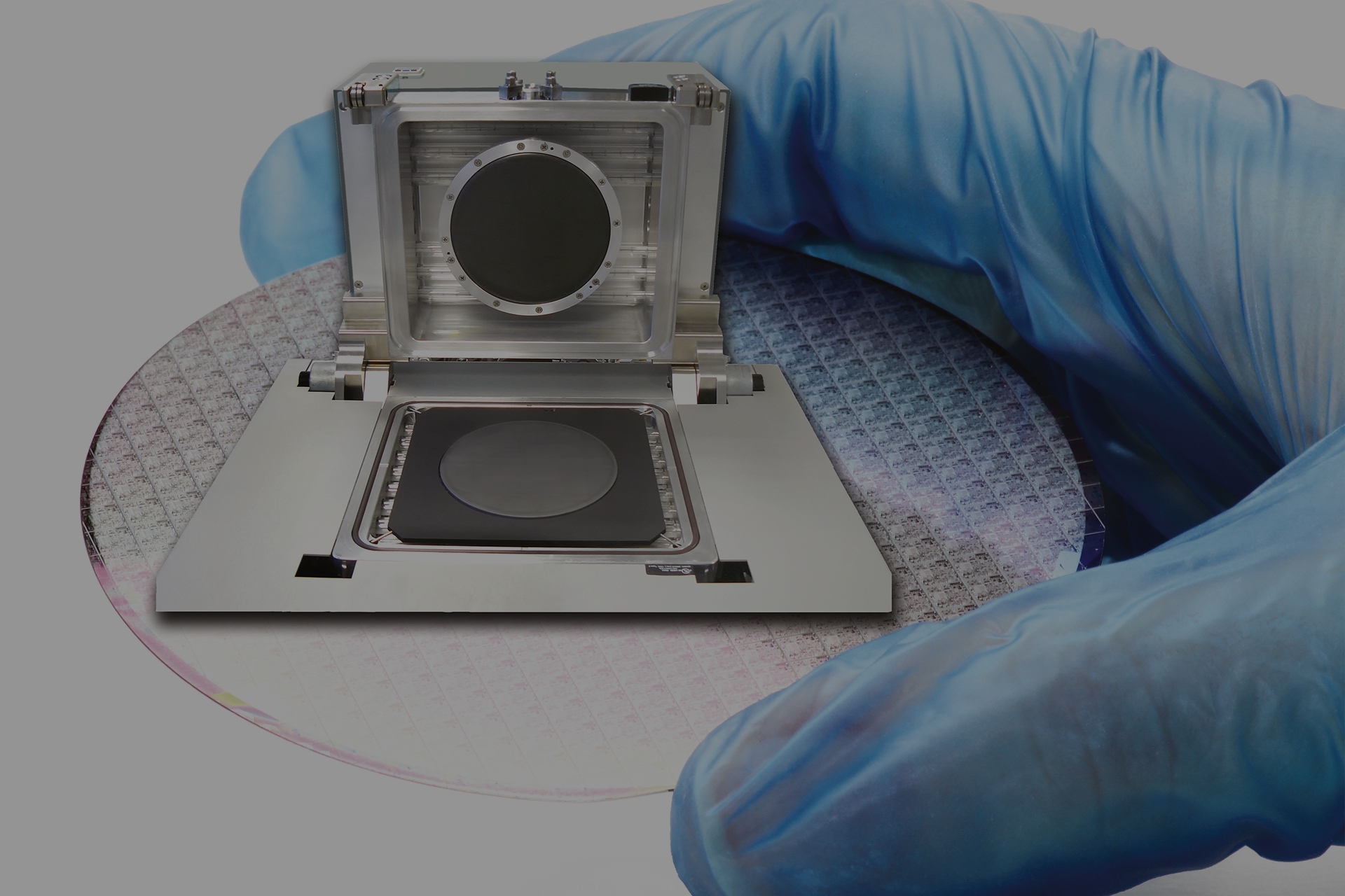
Newer, smaller semiconductors are frequently being designed to utilize ultra-thinned wafers, which present their own unique handling and testing requirements. Defects occurring throughout production, especially during the grinding and polishing (CMP process stages), may crack delicate die or set the stage for eventual device failures.
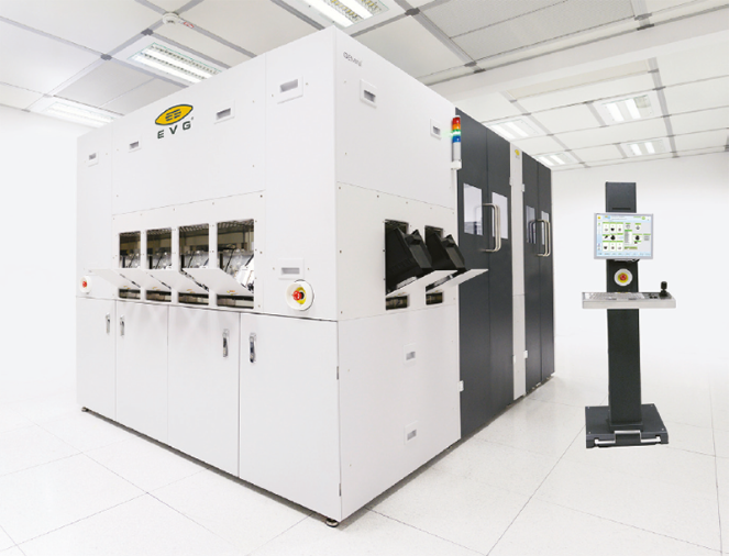
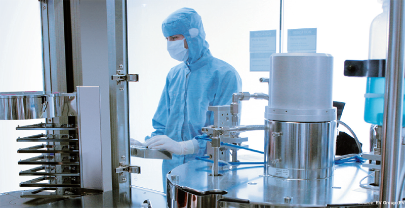
EVG GEMINI Automated Production Wafer Bonding System
UnitySC (Grenoble, France) is expanding thanks in part to the popularity of its 4See Series of devices that go beyond traditional backside wafer inspection. Designed to spot nanometer-scale defects, their approach utilizes phase-shift deflectometry (PSD) and conformal confocal (CC) inspection technology; Unity’s system is unique and patented. A number of customers are utilizing the UnitySC system for inspection of two-layer, bipolar IGBT power devices. The company expects greater growth potential as spotting more defects on the backside of a semiconductor as well as its top with one tool becomes more critical with each new device generation.
Another sign of expanding reliance on sophisticated inspection and metrology tools was an announcement by Rudolph Technologies in 2017 that its Firefly inspection system was selling briskly in China and that the first delivered devices had qualified to enter production. Firefly provides high-resolution visual and nonvisual inspection to support a variety of advanced packaging processes including fan-out wafer-level packaging, panel- and wafer-level CSP. Rudolph expected over (USD) $5 million in revenue in Q3 2017 from the systems.
As various next-generation device architectures move from design to production, 2017 also experienced growth in areas that are not traditionally seen as the sources of continual innovation: the sub-fab. Reno Sub-Systems (Reno, Nevada, USA) announced that its late-2017 funding round garnered (USD) $11.2 million in investments, which is not record-setting by itself, but interesting in the fact that major backers included Intel Capital, Samsung Venture Investment Corporation, Hitachi HighTech, sk Hynix (a South Korean memory chip powerhouse), Lam Research (that bought advanced modeling expert Coventor in 2017,) and MKS Instruments (USA, with offices across Asia, Europe and North America).
Reno specializes in two principal technologies: flow control for gases used in chip making and RF power generation with impedance matching of process electrical loads. Both of the company’s primary products offer substantial increases in performance compared to legacy solutions, and are targeting nextgeneration device manufacturing requirements where tightly controlled performance and faster production is more critical to a company’s success.
As more semiconductor manufacturers diversify their approach to future markets, this in turn drives responsiveness from vendors who are constantly challenged to develop new ways to address future requirements. One company responding with a growing product line is Brewer Science (USA) that provides materials and processes addressing key device architecture needs by reducing wafer stress, warpage, and high temperature limitations while also enabling faster throughput and reduced form factors.
Brewer Science’s temporary bonding and debonding techniques are especially applicable in fan-out wafer-level packaging (FO-WLP). While the ‘chip-first’ approach has been in high volume manufacturing for some while, the ‘chip-last’ approach is still developing. Brewer sees many of its product solutions as offering a complete range of options for customers, whichever approach they are taking.
Like other companies serving different segments of the supply chain, Brewer Science offers a wide assortment of options to fit the diversity found across global manufacturing. Brewer has supported temporary bonding/debonding requirements across multiple device generations and is one of the few companies to support every major type of physical debonding approach. Their products continue to evolve and now include fourth generation solutions for laser systems; they have succeeded in raising the temperature range of processes they can support up to 350° C.
“We have almost 15 years of experience in temporary bonding materials development and commercialization for the manufacturing of 2.5D, 3D, compound semiconductor, fan-out and other process flows. We realized very early that one product or even one platform of temporary bonding materials may not be suitable for all of the processes used in advanced packaging applications. Each process flow or device type has a unique set of requirements, and we offer a broad portfolio of bonding materials and release layers designed to support these individual processes. This approach results in maximized customer benefits, in terms of delivering simple processes with high yield and low cost of ownership,” said Ram Trichur, Director of Wafer Level Packaging Business Development at Brewer Science.
Trichur said that the company is seeing growing interest in the latest generation of tools, especially across Asia and most notably in China. While all customers see benefits, some report rather remarkable results, especially when they had previous solutions that were not delivering as needed.
“All of our customers benefit from the advances (we) deliver, yet some have particularly striking success stories. A manufacturer in North America that was producing compound semiconductor devices and bonding with wax materials had a total yield loss of around 30 percent during backside processing due to the poor thermal and mechanical properties of wax. We introduced a new temporary bonding material, and their yields subsequently increased to over 99%,” said Trichur.
In addition to solutions that increase accuracy of mask alignments and that enable processing of thinner films at lower temperatures, manufacturers are also looking to atomic level deposition (ALD) and its cousin, atomic level etch (ALE) to control materials removal much more precisely than in the past. Current etchants are typically used to remove materials across entire wafers, which is not always desirable. ALE offers greater accuracy and continual advancements in the field are redefining precision etching. Applied Materials sees their processes as complimentary with ALE, offering the customer even more control including a new approach under study that would enable the ability to ‘erase’ unwanted material without substantially delaying production, implementing EUV, or installing other leading-edge lithographic tools.
Directed Self Assembly (DSA) continues to gain interest as a means of supporting advanced node scaling while it also helps reduce line-edge roughness (LER). Brewer Science joined with Arkema Group in 2015 to facilitate high-volume production of first-generation DSA polymers. Arkema is a high performance materials specialist based in France with a global presence and 2016 sales of 7.5 billion euro. Brewer Science also is developing second-generation polymers that are essential to enabling DSA at future nodes. The partnership between Brewer and Arkema now seeks to commercialize these high-x (chi) block copolymers for DSA. First generation polymers supported devices down to 22nm while generation two research targets 5nm and below, which the company and most industry experts agree is critical to extending device scaling without relying on EUV or complex multi-patterning schemes.
“DSA represents a lower cost and higher throughput solution over EUV, but another big cost advantage lies in the reduced mask requirements. DSA still needs lithography and etch processes, but these are lower cost compared to multiple patterning. EUV masks are a significant part of the EUV step cost. DSA also offers a technical advantage that it can reach lower feature sizes now than other patterning technologies,” said Hao Xu, Director of Semiconductor Business Development at Brewer Science.
In addition to its cost advantages over EUV, Brewer indicated that it continues to explore DSA advantages because they see the process as complimentary with EUV. Companies that have already committed to EUV may conclude that combining DSA with EUV will better support their goals.
“DSA and EUV are complementary because smaller pitches can be printed with EUV that are not accessible with immersion litho. Smaller pitches means two things: lower multiplication factors can be done with DSA, which leads into lower possibility for defects. Also, there is the possibility of eliminating the trim etch step in the chemoepitaxy flow when using EUV. EUV can also provide graphoexpitaxy templates for contact hole multiplication. It is also important to note that because of the resolution limitations of EUV at smaller nodes, it is possible that DSA will help stretch out the timing for, or even eliminate, the need for high-NA (numerical aperture) EUV tools,” Xu added.
EMD Performance Materials (a division of Merck KGaA, Darmstadt, Germany,) continues to grow its commitment to advanced semiconductor processing materials science. Rico Wiedenbruch, head of the IC Materials Business Unit at Merck, said his unit is focused on the many scaling related challenges that the industry faces, offering a wide variety of novel solutions to meet these demands and solve miniaturization roadblocks that challenge the limits of physics. The company’s advanced precursors for atomic-layer deposition are a turnkey solution for producing very thin, highly controlled conformal films, he indicated.
The EMP portfolio extends to a number of areas for conventional semiconductor manufacturing including front- and back-end packaging. Wiedenbruch noted that EMP’s latest solutions target microprocessors, DRAM and NAND Flash memory and are being extended to support ALD precursors for memory devices and 3D NAND cells. He noted some of the biggest problems customers face have to do with pattern collapse, which they address with their FIRM line of processing rinse materials; they also offer block copolymers for DSA. Their line of RELACS Shrink Materials are designed to support the manufacture of devices with much more narrow features than was previously possible.
While materials suppliers are developing and proving resources for next-generation nodes, others are utilizing those tools to further advance such technologies as 3D stacking. CEA Leti (Grenoble) and EV Group (St. Florian, Austria), announced late in 2017 that they had achieved what both organizations believe is an industry first: a successful 300mm wafer-to-wafer direct hybrid bond with pitch dimension connections as small as 1µm (micron).

Fully automated A series wet bench from AP&S
Vertical stacking of semiconductor devices has become an increasingly viable approach to enable continual progress towards greater device density and higher performance. Wafer-to-wafer bonding is an essential process step in building 3D stacked devices. Tight alignment and overlay accuracy between the wafers is required to achieve good electrical contacts while minimizing the interconnect area at the bond interface. This is a critical factor since achieving it increases space for more viable die on each wafer, thus delivering higher yield. The constant reduction in pitches that are needed to support component roadmaps is fueling tighter wafer-to-wafer bonding specifications with each new product generation. The product demonstration at Leti’s facilities in Grenoble utilized an EV Group Gemini FB XT automated production fusion bonding system.
“To our knowledge, this is the first reported demonstration of sub-1.5µm pitch copper hybrid bonding feasibility,” said Frank Fournel, head of bonding process engineering at Leti. “This latest demonstration represents a real breakthrough and important step forward in enabling the achievement and eventual commercialization of high-density 3D chip stacking.”
Research into alternative approaches to transistor design and manufacturing is a robust activity at Leti, the imec group (Leuven, Belgium,) and multiple Fraunhofer institutes in Germany and elsewhere. One recent announcement from imec researchers involved gate-all-around nanowire field effect transistors (FETs) that they organized into a novel vertical configuration. This technology is considered a strong candidate to extend today’s CMOS scaling to its ultimate limit. With an excellent performance-to-area ratio, vertical nanowires seem particularly attractive for making highly dense static random access memory (SRAM) cells, imec notes. Moreover, when used to build those SRAM cells, vertical nanowire FETs may play a key role in hybrid scaling – an emerging approach that integrates multiple transistor architectures in one system-on-chip.
Nanowire FETs can be implemented in a lateral or a vertical configuration. Devices configured laterally still utilize conventional 2D layouts, which means they will eventually hit physical limits that are similar to the roadblocks that existing FinFETs are already experiencing. In the case of nanowires organized horizontally, the space available for gate and contact placement will become so small that the devices may no longer function effectively.
Moreover, in the back-end-of-line, too many metal lines in increasingly narrow spaces can give rise to interconnect routing congestion and the possibility of current leakage. Imec researchers believe these issues present an opportunity for vertical GAA nanowire FETs. With these devices, designs can move from 2D to 3D layouts, wherein the gate length is defined vertically. Such a disruptive innovation requires early process-design co-optimization, but it also means that the gate length can be more relaxed without consuming a larger area on the wafer. It also allows some relaxation in the nanowire diameter while preserving control over the short channel effects.
Conclusion
Traditional CMOS scaling has become increasingly complex and expensive, which has led semiconductor manufacturers to seek alternatives to meet demands for higher performance at lower costs. That drive includes the development of extreme ultraviolet (EUV) lithography to replace multi-patterning immersion litho; the latest EUV forecasts by ASML (The Netherlands) and mega-scale manufacturers Intel and Samsung indicate EUV is reaching stabilization.
Once implemented, EUV is likely to require additional refinement to extend the number of wafers per hour that can be produced with acceptable yields. Intel, Samsung and TSMC have all indicated they plan to utilize EUV at future technology nodes, varying between 7nm and 5nm.
At the same time, all major manufacturers are seeking alternatives for long-term device scaling that either avoids EUV altogether or delays its introduction. Scaling (with or without EUV,) below 5nm is possible. An increasing number of researchers, device manufacturers and materials experts are exploring alternatives to the ‘brute force’ scaling approach that previously served industry when moving to a new node meant a relatively simple exercise in miniaturization. The future of transistor design for high performance requirements will no doubt include a variety of approaches that could feature various 3D architectures using bonded and stacked devices, and alternative technologies such as fully depleted silicon on insulator (FD-SOI) championed by Globalfoundries, STMicroelectronics, CEA Leti and Samsung, among many companies.
Atomic scale deposition and etch will likely support these strategies as materials science continues to play a larger role supporting new architectures and processing techniques.
Multiple strategies are certain to emerge as effective means for enhancing performance while controlling costs within the global semiconductor marketplace. While major consumer product segments including smartphones, computing and entertainment are expected to continue driving memory and other high-performance applications at high volume, more opportunities are emerging that will require lower volume approaches and rapid customization.
Emerging applications such as the IoT, the IIoT, automotive electronics, medical and wearable electronics are shaping a new global semiconductor market and will continue to do so in the years to come.
The demand for mobile data is expected to increase seven times between 2016 and 2021. Silicon Semiconductor invited the head of IDLab, an imec research group at Ghent University (Belgium), to discuss the future of high speed mobile and fixed data transmissions. By: Professor Piet Demeester – Head of IDLab, an imec research group, Ghent University
The mainstream adoption of cloud computing applications and the projected, sevenfold increase in global mobile data traffic between 2016 and 20211 are just some of the recent trends that continue to boost the demand for high-speed broadband communications.
To cater for that need, the international research community has increasingly been focusing on advancing optical communication systems, using light to transport huge amounts of data from one place to another.

The need for (ever more) speed
To transmit those light beams – and the data they carry – optical communications systems make use of optical fibers; flexible, transparent (glass or plastic) fibers with a diameter slightly thicker than that of a human hair. Compared to legacy (copper) cables, they enable data to be transmitted over longer distances, considerably faster.
At the September 2017 European Conference on Optical Communication (ECOC), for instance, Japanese researchers presented a massive breakthrough in terms of how much data can be transmitted through a single optical fiber – reaching a transmission speed of 10 petabits (10 million gigabits) per second; a landslide achievement that will undoubtedly revolutionize the way in which intercontinental fiber-optic communication networks will be built and operated going forward.

Figure 1: Cisco Systems projects that the demand for mobile data traffic will increase seven times between 2016 and 2021.
In pursuit of these ever more powerful optical communication systems, increasingly faster and efficient optical transmitters and receivers at both ends of the optical fibers need to be developed. That is exactly one of the key strengths of our researchers at IDLab, an imec research group at Ghent University.
Breaking the barriers of fiber-optic communications Our research in this space aims at improving the performance of four technologies in particular:
In 2017, our teams contributed significantly to pushing the data rates that these technologies can accommodate. In the datacenter realm, for instance, the broadband speeds attained by our demonstrators run 5 to 10 years ahead of the Ethernet Alliance’s standards. And the same goes for our research into PON networks, where we currently achieve bitrates 5 times higher than today’s commercial solutions.
Figure 2: Imec and its IDLab research center are testing new approaches to optical communication. Shown is the testing environment of imec’s new ‘optoantenna’ that eliminates the conventional electrical amplifier previously required to create an RF signal.
New perspectives: radio-over-fiber
The radio-over-fiber (RoF) track is the latest addition to our research agenda, and will become increasingly important in the course of 2018. As mentioned already, RoF is poised to become an essential enabler of the wireless ‘small cells’ technology that already surrounds us today – with large amounts of wireless antennas that each cover a small area (or cell) to enable very high-speed wireless broadband. The smaller the cell, the higher the bitrates that can be attained.
The trend towards installing increasingly smaller cells is not new; but the tendency to aggregate more and more functionality from individual small cells base stations in a so-called ‘cloud radio access network’ (cloud RAN, also called centralized RAN) is new. Traditional cellular networks consist of many standalone base stations, with each of those base stations processing and transmitting their own signals to and from mobile terminals, and forwarding the data payload to and from the mobile terminal and out to the core network. Each base station has its own cooling, backup battery, monitoring system, and so on.
In a setting where growing numbers of small cells are being installed, the value proposition of a centralized RAN is obvious: as functionalities and hardware are shared, costs decrease. And RoF will be fundamental to making the communication between a cloud RAN and its remote antennas as easy and cost-effective as possible.
Up until today, this topic has not yet been explored in detail by the international research community – so we really have the potential to generate substantial impact in this domain. One nice example is the socalled opto-antenna we developed; a passive antenna that directly connects to an optical fiber; it no longer requires an (electrical) amplifier to produce an RF signal. With all of its active functionalities residing in the cloud RAN, our opto-antenna could easily be integrated in a number of materials (floor tiles, wall paper, etc.) for very high-speed wireless connectivity at short range. In our first tests, for instance, we achieved bitrates of 0.5 Gbps at distances up to 20cm. (Production Note: Figure 2 image should be located as close to the above text as possible)
The future is optical
In the next couple of years, the improvement and refinement of optical technologies will remain very high on our research agenda. If one needs to send lots of data over longer distances, it is clear that optics remains the way to go – not only in the wireline, but also in the wireless domain.
And our research into RoF will be fundamental to making this a reality. As wireless spectrum and spectral efficiency are reaching their scaling limits, deploying increasingly smaller cells will be key to continue to increase wireless bitrates. And more cost efficient technologies, such as RoF, will be required to accommodate this.
Thanks to a close collaboration with other imec research teams working in the area of wireless communications and photonic technologies and devices, we are uniquely positioned to contribute to this evolution.

Biography Piet Demeester
Piet Demeester is professor in the Faculty of Engineering and Architecture at Ghent University, IEEE Fellow and holder of an ERC Advanced Grant. He also heads IDLab, an imec research group at Ghent University and the University of Antwerp. After finishing a PhD on Metal Organic Vapor Phase Epitaxy for photonic devices in 1988, he established a research group in this area working on different material systems (AlGaAs, InGaAsP, GaN). This research was successfully transferred to imec in 2002. In 1992, Piet started research on communication networks and established the IBCN research group (now integrated in IDLab). IDLab is focusing on several advanced research topics: Distributed intelligence for IoT, Machine Learning, Data Mining, Semantic Intelligence, Multimedia Processing, Cloud and Big Data Infrastructures, Fixed and Wireless Networking, Electromagnetics and Transceiver IC Design for Optical and Optical-Wireless Networks.
A micro-transfer printing technique could boost the efficiency of integrated power electronics by uniting high-performance GaN HEMTs with highly integrated silicon CMOS by Stefan Eisenbrandt and Ralf Lerner from X-Fab
Lying at the heart of the majority of today’s power ICs are three classes of silicon transistor – those with either a laterally diffused metal-oxide-semiconductor design, an insulated-gate bipolar architecture, or a super-junction configuration. All these workhorses can handle high voltages, high currents, or a combination of both.
It is known from Moore’s law that miniaturising these transistors would deliver an evolutionary improvement in performance, but at the expense of spiralling development efforts. Better still is a revolutionary performance gain. This is possible, via the integration of III-V materials.
One of the most promising III-V devices for power electronics is the GaN HEMT. Compared to all forms of silicon device, it sports superior switching speeds, and it also has the upper hand when considering the trade-off between the on-resistance and the breakdown voltage. Thanks to these merits, the GaN HEMT can enable new, highly efficient power conversion topologies that would be unthinkable with state-of-the-art silicon based devices.
Let’s not write silicon off just yet, however. Note that bipolar-CMOS-DMOS and high-voltage CMOS technologies have realised high levels of diversification, leading to the highest design complexities. These devices can be used in Smart power ICs, which enable an interface between digital control logic and the power load. By using monolithic integration to position output power devices next to digital and analogue circuitry, it is possible to combine signal processing, sensing and protection circuitry on the same chip. Further benefits of this approach are a trimming of the number of interfaces, the volume, and electromagnetic interferences. The upshot is increased efficiency, performance and reliability.
Engineers working with compound semiconductor technologies are also trying to realise the high-level of functional integration seen in these silicon-based, Smart power ICs. Several technologies for integrating GaN HEMTs with digital and analogue circuitry are currently being pursued: GaN-based Smart power ICs; monolithic integration of GaN on silicon; wafer bonding of GaN on silicon; and the approach that we are investigating at X-FAB Semiconductor Foundries of Erfurt, Germany: heterogeneous integration, enabled by micro-transfer-printing (see Figure 1).
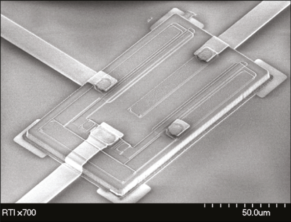
Figure 1. Micro-transferprinting can position a GaN HEMT on a silicon CMOS wafer, prior to subsequent on-wafer metallization.
Rival approaches
Several groups are working on integrating GaN power devices with GaN digital and analogue circuitry on the same substrate. The downside of this approach is the lack of feasibility of standard silicon-CMOS-like circuit topologies, due to an inferior hole mobility and the absence of high-performance p-channel GaN devices. Due to these weaknesses, it may take years to realise high integration densities and functional diversification with GaN-based logic.
Monolithic integration of GaN and silicon CMOS is another option for uniting GaN-based transistors with CMOS logic. Both devices can be fabricated on the same silicon substrate, with custom silicon-oninsulator wafers providing tiers for each technology: <100> oriented silicon for CMOS and <111> oriented silicon for GaN. The GaN and silicon transistors are not vertically integrated, but are arranged laterally side-by-side.
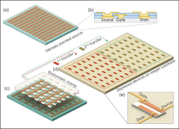
Figure 2. An overview of the micro-transfer-printing process for GaN HEMTs. (a) Source wafer with dense array of HEMTs, (b) HEMT cross-section, (c) elastomeric stamp removes an array of HEMTs from source wafers, (d) first and second printing process on new target substrate, for example a CMOS Wafer, (e) wiring of printed GaN HEMT on wafer.
A team from Raytheon has pioneered this approach. To reduce the thermal budget, they deposited the GaN layers by MBE, rather than MOCVD. The price to pay for this is a lower throughput, making this approach unfavourable for mass production of higher voltage devices, which require thicker buffer layers.
Additional drawbacks of this approach are: material incompatibilities, such as significant differences in lattice constants and thermal expansion coefficients; device constraints, such as thermal budgets and the restriction of contact metallization materials to CMOScompatible metals; and high costs. Note that due to the partitioning issue associated with monolithic integration, costs can skyrocket. For example, for an integrated circuit with a total area of 10 mm² – comprising 9 mm² of logic and 1 mm² of GaN HEMT – the costs for the epitaxy process are similar to those for a full-wafer process, but the epitaxial layer is only used on the 1 mm² GaN area. Thus, the costs per GaN area, and also the costs per Amp, are ten times higher.
Another option for combining the merits of GaN power devices with those of silicon CMOS is to fabricate each in its dedicated manufacturing environment, before uniting them densely at the chip level. With this approach, every device is designed to its full potential, irrespective of material and processing constraints. That’s because integration takes place by wafer bonding in a post-process step.
We have been pursuing this type of approach through a multi-partner project GaNonCMOS, funded by the European Union’s Horizon 2020 Research and Innovation programme. Supported by €7.4 million of investment, this effort that kicked-off in January 2017 is aiming to bring GaN power electronic materials, devices and systems to the next level of maturity by providing densely integrated materials. A key goal within the project is to realise long-term reliability improvements over the full value chain of materials, devices, modules and systems.
Micro-transfer printing
One of the key technologies in our project is microtransfer-printing. Like wafer bonding, it facilitates the post-process integration of GaN power and silicon CMOS devices, but it also allows the deterministic assembly and integration of microscale, highperformance semiconductor devices onto non-native substrates.
The key process with micro-transfer-printing is the picking-up of large arrays of microscale devices from their source wafer with an elastomer stamp, and the subsequent printing of these devices on a retrieving wafer. This is accomplished by housing the stamps on high-precision, motion-controlled print-heads. With this parallel process, many small chiplets carrying GaN HEMTs can be printed onto fully processed silicon CMOS wafers in one go (see Figure 2).
The majority of GaN HEMTs are grown and manufactured on <111> oriented silicon wafers. To prepare them for the micro-transfer-printing process, these devices then need to be released from their native substrate.
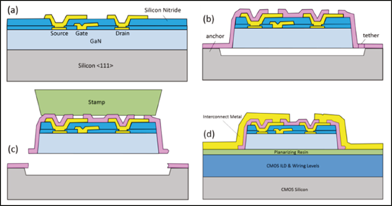
Figure 3. The process flow for heterogeneous integration of GaN HEMTs. (a) The transistors are fabricated on a <111> silicon substrate. (b) The devices are isolated, passivated and then undercut. (c) The devices are retrieved with an elastomer stamp. (d) The devices are printed to a silicon CMOS wafer and then interconnected using thin-film aluminium traces.
In the project that we are involved with, this step is undertaken by reactive ion etching through the device layers and down to the underlying silicon substrate (see Figure 3 (a)). Then, to passivate the sidewalls and form an anchor that tethers the structures, a SiN layer is added by plasma-enhanced CVD (see Figure 3 (b)).
After this, the <111> oriented silicon underneath the device is wet-etched using a high-selective, anisotropic etchant (see Figure 4 (a)). As the etch rate in the {110} family of directions is more than one hundred times faster than it is in the orthogonal directions, regions where the silicon does not undercut remain as anchors for the release process (see Figure 4(c) for an optical microscope image of two fully undercut, print-ready GaN HEMTs with different tether configurations).
Utilising the viscoelastic nature of the elastomer stamp, GaN devices are then picked-up from their source wafer and printed on the CMOS wafer. Due to the high adhesion between the stamp and the GaN device, when the stamp is then moved rapidly away from a bonded interface, the tethers are broken, enabling the pick-up of microscale devices from their native substrates. A different approach is used to print the devices. This time the stamp is gently moved away from the bonded interface, causing the adhesion between the stamp and the device to be lower than that of the bond forces. Due to this, the stamp separates from the chips, which stick on the new, non-native substrate.
Following the micro-transfer-printing process, interconnections are added with standard wafer fabrication processes, such as thin-film deposition and photolithographic patterning (see Figure 3 (d)). With this approach, which involves on-chip wiring, process temperatures do not exceed 175 °C, permitting the use of complex Smart power designs.
Promising results
Small GaN HEMTs have been manufactured with various gate finger configurations, channel widths and gate-to-drain spacings (see Table 1 for an overview). All of these HEMTs have been produced with the same set of processes, and made from the same substrate wafer, which features a GaN epitaxial structure that is about 4 μm-thick. Using the processes described above, the HEMTs have been transferred to two types of wafer: completely processed silicon CMOS wafers; and trench-isolated, silicon-on-insulator high-voltage CMOS wafers.
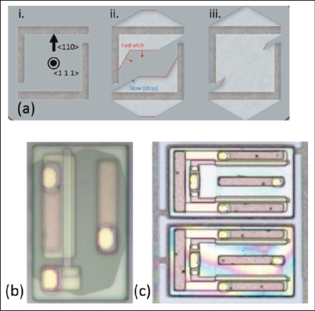
Figure 4: (a) Silicon <111> wet-etching underneath a device. (b) The etch-fronts can be seen by looking through a GaN HEMT that is only partially etched. (c) Optical micrograph of GaN HEMTs that have been fully undercut, with two different tether designs.
The benefits of printing HEMTs directly on top of CMOS are not limited to a smaller footprint for the final device – they also enable shorter wiring between the logic and the HEMT, reducing parasitic inductances and capacities (see box “Strengths of micro-transferprinting” for a detailed list of benefits).
Initial results include characteristics for a 20 V NMOS transistor that are undisturbed by the printed HEMT, and promising room-temperature, drain-source blocking mode characteristics for the printed GaN HEMT device (see Figure 5). Using a fluorinert protection layer to avoid surface flash overs and premature breakdowns, printed HEMTs have achieved blocking voltages of between 600 V and 1800 V, dependent on the drain-gate spacing.
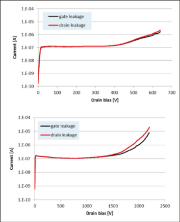
Figure 5: Blocking characteristic of HEMT with gate-to-drain distances of 6 μm (top) and 17 μm (bottom).
During the release etching, the conducting silicon substrate is removed, allowing the printing of the HEMT on top of the isolating CMOS dielectric. This eliminates a vertical leakage path through the silicon, and it restricts the breakdown mechanism, so that breakdown only occurs laterally in the GaN. Due to this, the breakdown voltage is solely determined by the gate-drain distance.
Another task undertaken has been to carry out a thermal TCAD Design of Experiment, in order to identify the main contributors to the thermal resistance of GaN HEMTs printed on top of a CMOS circuit. This effort revealed that there is only a small increase in the thermal resistance due to the CMOS dielectric layers – it is far less, for example, than the thermal contribution of wafer and metallisation thickness. Under AC conditions the thickness of the HEMT has a larger effect on the thermal resistance than the CMOS dielectric layers. Consequently, if silicon is removed in the manner that we have described, along with possible thinning of the GaN buffer layers, the CMOS oxide layers do not increase the total thermal resistance.
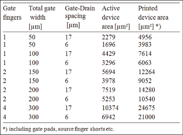
Table 1: GaN HEMT geometry overview
The results detailed here have been achieved within device level investigations. The next steps will be undertaken in an ongoing project MIIMOSYS, funded by the German ministry for education and research.
This project – involving Electronic Design Chemnitz GmbH, Fraunhofer Institute for Applied Solid State Physics, TURCK duotech GmbH (TDU), University of Erlangen-Nuremberg, Chair of Electron Devices, and X-FAB Semiconductor Foundries with support from X-Celeprint – is targeting the first ever demonstration of hetero-integrated GaN transistors onto silicon CMOS control electronics at the system level. Topics of future investigations will be the next steps towards a manufacturing process for micro-transfer-printing, the reliability of the involved GaN and CMOS devices and the packaging of micro-transfer-printed devices for bridge drivers and controller ICs for motor and LED driver applications.
Strengths of micro-transfer-printing
THERE are many merits associated with micro-transfer-printing:

Current scaling versus transistor width for GaN HEMTs in two voltage classes
Further reading
T. Erlbacher; “Lateral Power Transistors in Integrated Circuits”, Springer, Heidelberg New York Dordrecht London, 2014 “Power GaN Devices”, edited by Matteo Meneghini, Gaudenzion Meneghesso, Enrico Zanoni, Springer International Publishing, 2017
“Smart Power ICs”, edited by Bruno Murari, Franco Bertotti and Guiovanni A. Vignola, Springer International Publishing, 2002 R. Reiner et al., “Monolithically-Integrated Power Circuits in High-Voltage GaN-on-Si Heterojunction Technology“, IEEE, 2016 T. E. Kazior et al., “High Performance Mixed Signal and RF Circuits Enabled by the Direct Monolithic Heterogeneous Integration of GaN HEMTs and Si CMOS on a Silicon Substrate”, IEEE, 2011
Arm is the critical player in the global semiconductor market. While it does not manufacture its own chips, its processor designs enable approximately 100 billion silicon chips, powering products from the sensor, to the smartphone to supercomputers. It is also estimated that approximately half of the 5.1 billion Arm-based chips are for industrial uses. By: Nisarg Desai, Director of Product Management, IoT, GlobalSign
Like any semiconductor company, Arm (now owned by Japan’s SoftBank) is very much focused on security, and has a company-wide mandate to ensure secure products across the board from the chip up to the cloud.
Arm recently announced its ‘Platform Security Architecture’ initiative, aimed at providing security guidance for IoT device developers. It has four recommended security tenets, one of which is certificate-based authentication, a market that is expected to grow in the coming years. This is not a surprise given the current trends reported by The Ponemon Institute, one of the world’s top providers of research on the information security industry. Its 2017 Public Key Infrastructure (PKI) Global Trends Study, which gathered input from more than 1,500 IT security practitioners worldwide to determine where PKI is heading, found that 43 percent of IoT devices will adopt digital certificates for authentication within the next two years.

GlobalSign has long been a provider of PKI-based solutions, because it is time-tested, open standards-based, easily implemented and a widely accepted technology. PKI is even more relevant in this case, because it lends itself very well to IoT devices. It can be implemented in a relatively lightweight fashion on different classes of devices. Most IoT devices, by definition, are data gatherers, data transmitters and sometimes, data processors. Thus, secure communication is very important to IoT devices, and PKI is a simple and cost-effective way to achieve this. Asymmetric cryptography, which forms the basis of PKI, is mathematically and empirically proven to be an effective means of providing secure distribution of encrypted messages to targeted senders.
Security chips
Chip enabled and accelerated functions form the bedrock of most secure software and hardware implementations today. For example, the core identity of any device is stored in something called a Secure Element, a chip that forms the root-of-trust for a device. It serves as a Trust Anchor, which then enables other security functions such as Secure Boot and Remote Attestation. Many of these functions require a great deal of processing power – hence dedicated cryptographic chips accelerate these operations, making them faster and/or enabling them to consume less power. Quite a few of these chips are based on Arm designs. It is important to understand there are various options to adding a secure element. A Trusted Platform Module (TPM) chip is a crypto co-processor that sits alongside the primary processor and requires a redesign of the board to allow its integration. A more novel, equally secure but much more cost-effective option is to use a (Physically Unclonable Function (PUF). There are various other options, but discussing these in detail is out of scope of this article.
PKI for IoT devices
PKI’s roles, policies, and procedures are needed to create, manage, distribute, use, store, and revoke digital certificates and manage publickey encryption. PKI has been relied upon since the 1970’s and was first used in technologies such as e-signatures in the 1990’s. Today, it is viewed as one of the most reliable ways to secure IoT devices. All IoT devices require a strong identity and need to prove that they are who they claim to be, and not something else. This identity should be universal and easy to verify for the communicating party. Soon, they will even generate their own identity and store it safely, directly as a result of PKI’s unique mathematical capabilities. Also coming soon are IoT devices that will each have their own individual and unique certificate to prove their trustworthiness. By using PKI in this fashion, IoT devices will be more trustworthy, limiting the chances of unauthorized access.
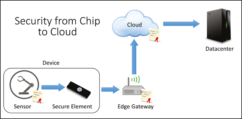
PKI enables ‘lightweight’ IoT security from chip to cloud. Image courtesy of GlobalSign.
Chip to cloud security
As alluded to earlier, Arm has a directive to ensure security across the board, from its chips, through their IoT stack, and up to the cloud embedded onto a chip. Arm takes its own low power Cortex-M product family and adds support for its open-source Arm Mbed OS embedded operating system. This combination is easy to use and to configure out of the box, making it ideal for small scale developers designing an IoT device and are at the stage where they are ready to begin creating design applications – they can simply use Mbed OS as their embedded operating system.
The Arm Mbed family also includes a cloud platform as a service, called Mbed Cloud. Since most IoT use cases today involve collecting sensor data from an IoT device on the edge and then transmitting it up to a cloud application for further processing, this cloud service is very useful. Mbed OS can natively integrate and connect to Mbed Cloud. Now, Transport Layer Security (TLS) is the protocol of choice for most device to cloud connections. This requires the use of digital certificates.
What is significant about Mbed Cloud is that it supports a “bring your own Certificate Authority (CA) program.” You can have a third-party CA create a dedicated PKI hierarchy and upload the Root CA Certificate to Mbed Cloud. This enables certificatebased authentication to automatically accept connection requests from all your devices that have a certificate issued from that particular hierarchy.
Getting started
A very important first step for IoT device developers is enabling security across the vertical IoT platform stack – right from the end device or sensor node, through the edge and fog layers, up to the cloud-platform and underlying data and application infrastructure. This can be achieved by ensuring that, as data is passed through these layers, each step in the chain is verifying it is communicating a party’s identity and authority, while ensuring data privacy and integrity. This is attainable through PKI.
For those not intimately familiar with PKI, it is a commonly used approach to encryption and authentication. The architecture provides a greater level of confidence for sharing information electronically. First, we can look at how devices can ensure integrity within themselves. One way to achieve this is Secure Boot. A Digital Signing Service can be used to sign and compute the hash of any firmware, before loading onto the device. The public key used to sign the firmware is stored on the device, in non-erasable memory. Whenever the device boots up, a hash of the bootloader (the process of applying an algorithm to generate a small string from a larger file that can later be used to verify the file’s integrity) is generated and signed by the public key. Now if we can trust this public key, and verify this signed record to be accurate, then we have proved that the bootloader (and anything else that was checked) is genuine. If we then send this signed report or file to a remote server, periodically, to prove that the bootloader is genuine, we have remote attestation.
Heralded for its unique properties for advanced semiconductor manufacturing and many industrial processes, synthetic diamond from Element Six has found a new home treating some of industry’s most toxic waste water.
Globalized heavy industry has largely contributed positively to modern economies by creating employment and providing low cost finished goods. However, many industrial processes also create large volumes of concentrated hazardous waste water, some so harmful that it is difficult to handle, let alone dispose of safely. Sometimes they are simply diluted down and allowed to enter conventional water treatment processes.
The solution to this growing tidal wave of toxicity? Synthetic diamond.
Toxic waste water isn’t just a problem in long-industrialized countries. Neither is it limited to emerging economies who welcome some types of manufacturing without fully understanding the harmful impact of waste waters that they can generate, or the consequences of safely handling these effluents. A solution now exists to treat in situ those wastes associated with toxic dissolved organic compounds that issue from a wide number of industrial processes and chemical manufacturing.
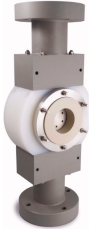
Figure 1: The Element Six ‘bolt-in’ waste treatment unit comprising a Diamox cell with solid BDD electrodes, housing and all electrical and pipework connections is delivered ready to install into Electrochemical Advanced Oxidation Process (EAOP) systems.
Technical editor for Silicon Semiconductor, Mark Andrews, spoke with Tim Mollart (PhD), Principal Applications Engineer at Element Six, about the hardware and materials technology underlying the treatment cells his company calls ‘Diamox.’ Mollart leads the research and application of his company’s synthetic boron doped diamond electrodes, including their use in the Diamox system.
Originally introduced in 2016, Diamox is Element Six’s second-generation technology, a cost-effective and efficient wastewater treatment electrochemical cell, designed using freestanding, boron-doped diamond electrodes. Diamox is effective in removing the dissolved organic content of contaminated industrial wastewater that cannot be treated using biological methods. Element Six describes its packaged reactor as simple to implement in on-site advanced oxidation technology, providing an environmentally cleaner and versatile solution that can be used across various types of effluents. There are no hazardous chemical additions and therefore no solid residue or sludge.
Mollart said that Diamox has been successfully implemented in pilot projects with an industryleading wastewater treatment company, delivering electrochemical advanced oxidation capacity that can be scaled to meet industrial requirements. The company is now in the process of widely marketing the technology, since its amassed data establishes Diamox’s effectiveness in multiple, real-world situations.
Mollart further explained that while biological treatment processes are adequate when handling simple organic and inorganic compounds, the situation changes completely when recalcitrant compounds such as phenols are introduced into waste streams. Further, that biological processes (such as those found in municipal water treatment systems and across industry,) are easily upset or rendered ineffective when ammonia, nitrates, and phosphates—all common to multiple industries including semiconductor manufacturing—are present within waste streams.
Advanced oxidization processes (AOPs) have been utilized by industry since the 1990s, to deal with some of the most difficult compounds found in waste streams. Often these work by combining UV or electrochemical activation processes with strong oxidizing chemicals such as hydrogen peroxide or ozone to generate the hydroxyl radical, which has the oxidative power to mineralize these recalcitrant species. What Mollart called an ‘attractively simple route’ to avoiding the addition of more chemicals to an already complex mix has been enabled through the use of diamond electrodes.
The electrodes directly oxidize hydroxyl ions - occurring naturally in water - to create the hydroxyl radicals on the surface of the electrode. All other types of metal-based electrodes are less effective since they are rapidly self-consumed by any hydroxyl radicals that they generate. Diamond passes the tests that other materials fail thanks to its unique properties that make it such a highly prized industrial workhorse. Its extraordinary chemical inertness enables the hydroxyl radical to exist for a few critical nanoseconds on the surface of water undergoing treatment and be available to oxidize dissolved pollutants in wastewater streams.
So why isn’t the world already using synthetic diamond reaction elements to treat its most hazardous waste? Early generations of thin-film diamond electrodes, created for use in electrochemical advanced oxidization processes, were uncompetitive in a price-sensitive industry. This was due to their oxidation capacity and production costs when compared to alternative advanced oxidation water treatment techniques.
Figure 2: (Left) Diamox contains a stack of bipolar BDD electrodes to maximize the effluent’s exposure to oxidizing species generated at the electrode surface.
Beyond these issues, a key failure mechanism also existed in earlier types of diamond electrodes relative to applications in wastewater treatment. Earlier processes utilized substrates that would dissolve in common treatment applications. These factors largely delayed development until companies like Element Six pioneered more effective means for cost-effectively manufacturing diamond electrodes. The microwave plasma-enhanced CVD reactor process that Element Six developed can be used to create high-purity, freestanding boron-doped diamond.
The high deposition rates that can be achieved by Element Six’s synthesis technique enables selfsupporting, freestanding, high-purity diamond electrode fabrication. With no substrate to be dissolved by the hydroxyl radical, the primary failure mechanism that plagued older thin-film diamond electrodes was eliminated. A further benefit of switching synthesis techniques is that solid boron-doped diamond (BDD) electrodes have a wider solvent window, enhancing electrochemical processing efficiency. While high-rate deposition techniques are limited by the area, this is mitigated by the ability to operate the electrodes at 10 to 20 times the current density when compared to conventional electrodes. The work done is proportional to the total charge flowing through the cell. A significant advantage of solid diamond electrodes is their ability to operate at <10,000 Am-2 without the loss of effectiveness; this dramatically lowers the consumable costs when expressed per kilogram of COD removed.
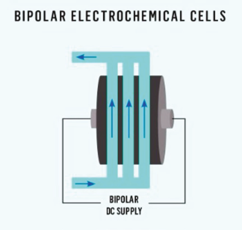
Figure 3: Diamox uses BDD for the anode and the cathode. The design allows for switching the polarity of electrodes to prevent fouling, enabling operation in highly contaminated environments.
Now that the stage was set for synthetic diamond electrodes to play a role in cleaning-up industry’s more toxic waste products, Element Six had to demonstrate cost-effectiveness and viability compared to other treatment scenarios. When selecting an advanced oxidation technique, physical plant operators typically consider consumable costs as a critical factor. In the case of electrochemical advanced oxidation, the dominant cost is the electrical power used to generate the hydroxyl radical and the consumable cost of the diamond electrodes. The amount of energy used to mineralize dissolved organic pollutants, expressed in kilograms of oxygen demand, into carbon dioxide (CO2) is in the range of 20 to 60 kWh, depending on the conductivity and concentration of the dissolved contaminate of the effluent.
Figure 4: The COD reduction of dissolved recalcitrant is demonstrated over time.
To maximize the utilization of the oxidation capacity of solid diamond electrodes, ultra-compact electrochemical cells are needed. Bipolar cells (see Figure 3) that can be operated in either polarity is preferred since other electrodes cannot survive in these conditions; fouling during contact with industrial effluents can occur. Cell materials that are capable of operating at pH extremes are also preferred due to the nature of industrial effluent they will experience. Solid diamond electrodes are preferred since they can be operated in extremely oxidative or reductive effluents. Supporting robust but brittle electrodes while enabling high recirculation flow rates, up to 25 m3 h-1, requires a significant engineering development process.
In determining the final element of cost-effectiveness - mass transport characteristics - Mollart said that one needs to review the measured rate of removal of dissolved organics (expressed as the coefficient of oxygen demand [COD]) removal, and map these characteristics (see Figure 4). The process maintains high efficiency throughout higher levels of concentration and is at its most efficient. Like any system, this decreases somewhat over time until the dissolved species are fully depleted.
Figure 5: EAOPs are compact and simple water treatment systems. The effluent is held in a process tank and then pumped through the Diamox cell.
Conclusion
Electrochemical advanced oxidation with solid diamond electrodes is an environmentally friendly method for treating waste streams. In particular, streams contaminated with toxic and persistent chemicals such as herbicides, pesticides, chloroand nitrophenols, polychlorinated biphenyls, pharmaceuticals, and other hard-to-treat compounds. Diamox has demonstrated its effectiveness in the treatment of a wide range of complex compounds, including high COD and ammonia-containing streams (such as landfill leachates), as well as for treating process waters used in many manufacturing environments. These include waste waters from oil and natural gas exploration and production. The Element Six Diamox solution is well suited for low volumes of waste streams containing high concentrations or recalcitrant COD that otherwise overwhelm treatment programs utilizing hydrogen peroxide and/or ozone.