
MAKING PLANS comes easily at the beginning of every new year. There is a fresh start, a blank new calendar, and it’s only natural to wonder what we should aim to achieve, and how best to fill our time.
Now caught up in a pandemic, planning can take a back seat. After all, when travel is discouraged, there may seem little point compiling a list of conferences to attend, or deciding when we might visit a company that we are collborating with. But there is no reason to get caught up in too much negative thinking. Vaccinations are now rolling out, and when spring turns to summer we will edge closer to normality.
Although 2020 has been a very tough year for most of us, the pandemic has not hit our industry that hard – and in some cases it even provided a silver lining to some very grey clouds.
To discover those sectors boosted by the virus, and those that took a minor hit or continued along an existing trajectory, I spoke to Yole Développement. Initially focusing on SiC, over the last decade this market analyst has expanded its activities, and now covers all the majors sectors within the compound semiconductor industry.
It’s of no surprise that sales of the UVC LED have blossomed over the last few months. If a bacteria-killing source can’t prosper in a pandemic, it’s never going to succeed. What’s encouraging, through, is that the analysts at Yole are predicting that this market will continue to thrive well after the vaccination programme is over, with sales climbing from just over $300 million in 2020 to $2.5 billion in 2025.
Far harder to foresee has been the positive impact of the pandemic on SiC power devices. A significant chunk of sales of this class of chip come from the electric vehicle sector, which forms a small but growing part of the automotive industry that has suffered from falling sales, now that many of us no longer have a daily commute. Governments from all around the world have been stepping in to support the car market, providing incentives for us to go out and buy an electric vehicle. According to Yole, by 2025, electric vehicles will account for more than 60 percent of a SiC market that will have mushroomed from below $1 billion this year to more than $2.5 billion come 2025.


How an up and coming silicon photonics start-up plans to take on a soon-to-be multi-billion dollar industry.
BY REBECCA POOL
BACK IN 2020, UK-based Rockley Photonics won $50 million in investment funds to grow its silicon photonics manufacturing technology, crucial for integrating III-V materials to silicon photonic integrated circuits. Investments now total more than $225 million, with the platform ready to take on large-volume production of high-density photonics circuits, including optical fibre and datacentre communication transceivers.
As chief executive, Andrew Rickman, says: “The latest funds are testament to the strength of our technology... We’re on track for the big wave of 400G transceivers and believe we’ll be in a pre-eminent position for the further wave of 800G transceivers for data centres.”
The timing of the funding isn’t surprising. Over the next few years, the global silicon photonics market is expected to mushroom, with analysts unanimous that this sector will be worth at least $3 billion come 2025 to 2027.
US-based Research and Markets predicts a mighty $3.77 billion by 2027, Global Market Insights, US, forecasts $3 billion by 2026, while Yole Développement of France, reckons the silicon photonic transceiver industry will be worth $3.6 billion come 2025. Today’s market comes in at around $800 million.
Growth looks set to be largely fuelled by increasing demand for high-speed broadband services and deployment of 5G technologies and data centres worldwide, including developing nations, with applications such as LiDAR also emerging in the automotive sector. And like its competitors, Cisco, Intel, Macom, Mellanox, Neophotonics and more, Rockley Photonics is intent on capturing market share here.
However, Rickman and recently appointed chief commercial officer, Vafa Jamali, also believe the healthcare and wellness sector holds huge promise, with the company developing optical sensing chipsets for handheld and wearable devices.
Jamali spent more than 25 years working in the medical device industry, most recently at US-Ireland based Medtronic, and reckons that while home health has been an emerging trend for some time, the pandemic has accelerated demand.
“So many people now want to have a lab on their wrist [that provides] accurate and meaningful measurements that they can trust,” he says. “This market is enormous and is growing at up to a 10 percent CAGR – I think there’s a great opportunity to disrupt with a better technology, and we reckon we have something that can do this.”
“So that’s my thesis for coming to Rockley after 28 years in medical devices,” he adds. “There’s nobody that aggressively addresses this market [with non-invasive devices], I am excited.”
Rickman is equally bullish, and highlights how wearables and smartphones are addressing a $45 billion market right now. “In our journey of 30 years in silicon photonics, we’re always looking out for that massive opportunity, and we know that anything that really gets driven by an economy of scale is in a consumer market,” he says. “So we saw this opportunity in devices for health and wellness – we believe that this is by far the single biggest opportunity in the field of silicon photonics.”
Winning formula
But how does Rockley Photonics intend to compete with industry players such as Cisco and Intel? Rickman is no stranger to tech giants.
Cisco and Intel each invested $10 million in Bookham Technology, the silicon photonics components business he founded back in 1988. Meanwhile, the company he chaired from 2008, Kotura, was acquired by Israeli-American computer networking multinational, Mellanox Technologies, for its 100G photonic ICs in 2013.
Since launching Rockley Photonics, in 2013, Rickman has asserted that the company’s ‘third generation’ silicon photonic platform is very different to the technology he helped to pioneer, and is offered, by rival firms. While most existing technologies integrate photonic structures with CMOS on a semiconductor chip, Rickman describes Rockley’s silicon photonic process as ‘engineered from the ground-up and optimised for photonics and not electronics’. And the platform still runs in large-scale silicon foundries.
According to the chief executive, difficulties arise when using a CMOS approach to integrate photonics structures at sub-micron dimensions as the wavelength of the photon is of the order of a micron. Rockley’s platform counters this in a number of ways, including the use of multi-micron waveguides that lead to lower waveguide losses and more consistent performance.
The platform also: eliminates the need for active precision fibre alignment, a key stumbling block in the manufacture of transceivers; efficiently integrates III-Vs; removes expensive specialised processing techniques; and can pack a large number of components at high density. Indeed, in 2018, Rockley demonstrated how its technology could cost-effectively make high-density optoASICs for datacentre switching.
China links
But beyond the different platform approach, Rockley also hopes to have an edge on its competitors by having a foot in the Chinese market with its joint venture with optical fibre and cable provider, Hengtong Optic-Electric. The partners are manufacturing 400G optical transceiver modules based on Rockley’s silicon photonics technology.
“We also realised that to be competitive we needed to take a vertically integrated approach to the market, and the Hengtong joint venture enables this,” points out Rickman. “So we’re now ramping up and shipping chips to our customers.”
Indeed, the timing looks right and the market is growing. The silicon photonics industry has already shipped millions of units of optical transceivers, and beyond Hengtong, other China-based companies have entered the market.
For example, Chinese cloud computing business, Alibaba Cloud, teamed up with US-based and Nokia-owned silicon photonics developer Elenion Technologies to manufacture a 400G optical transceiver. And China-based optoelectronics device provider, Broadex Technologies, has also joined forces with German start-up Sicoya, which manufactures silicon photonics transceiver chips.
Rickman is excited. From word go, Rockley has been working closely with large silicon and III-V materials foundries, as well as packaging facilities, preparing for the all-important ramp to large-volume manufacture.
“We believe that we now have the lowest cost technology and the lowest cost business structure to address a market of a particular time, including this extraordinary opportunity in health and wellness,” he says. “Next year is going to be all about ramping up production and from there on in we expect volumes to grow significantly.”

Andrew Rickman: Founder, Chairman & CEO of Rockley Photonics


Compact spectroscopic infrared sensors could aid healthcare, farmers, and sportsman.
BY KRISTIJONAS VIZBARAS FROM BROLIS SENSOR TECHNOLOGY
Think of infrared chips and you’ll probably think of InP. That’s because this material and its related alloys have had tremendous success in this spectral domain, providing countless lasers and detectors for long-distance optical communication.
But InP can only get you so far. While it’s the number one choice in the near-infrared, if you want to go further in that direction while retaining inter-band transitions, you’ll need to consider another class of material. And providing the best choice is the GaSb system, which is paving the way towards an optical sensing revolution.
Merits of GaSb and its related alloys include an accessible spectral range spanning 1.5 µm to 4 µm – this is rich in strong, specific combinations of fundamental absorption bands associated with molecular rotational-vibrational transitions (see Table 1 for comparison). In addition, this material system enables high-volume, scalable manufacturing of efficient light sources and detectors that operate at room-temperature and can be integrated with SOI-based PICs.
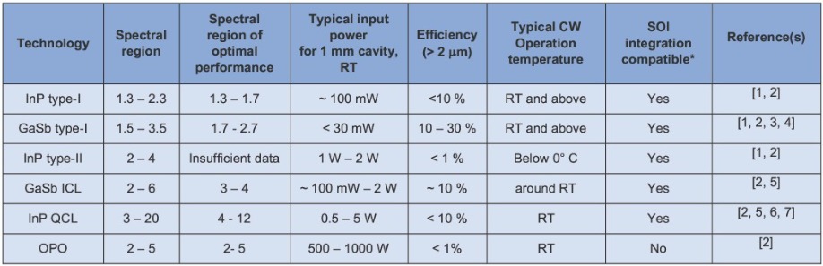
Table I. Comparing different technologies for infrared lasers underscores the merits of GaSb. [1] R. Wang et al. Sensors 17 1788 (2017) [2] S. Sprengel et al. Semicond. Sci. Technol. 31 113005 (2016) [3] K. Vizbaras et al. Proc. Of SPIE 8277 82771B, (2012) [4] K. Vizbaras et al. Appl. Phys. Lett. 107 011103 (2015) [5] A. Spott et al. IEEE Photonics Conference 2017, October 10, 2017 [6] M. Razeghi et al. Optics Express 23 8462 (2015) [7] M. Vitiello et al. Optics Express 23 5167 (2015)
Evaluating emission
For the GaSb material system – just as is the case for InP and its related materials – various options are available for generating laser emission. The most common is to use a type I quantum well, but for longer wavelengths interband cascade transitions may be needed. The pros and cons of these approaches, alongside alternative material systems, are outlined in Table 1.
Glance at this table and it is clear why the antimonide-based materials system is preferred, and why type-I technology is the best choice for high-volume applications that benefit from low energy consumption. Strengths include a mature design, high gain that results from the largest possible overlap between electron and hole wave-functions, and direct wafer-level testing of key electrical, optical and structural parameters – they include current-voltage characteristics, electroluminescence, and high-resolution X-ray diffraction spectra that offer an insight into strain, composition, and layer thickness. Having the opportunity to scrutinise a wafer before it is taped-in to make a device provides reliable early control of manufacturing yield, and allows pre-selection of wafers meeting the requirements to allow further processing.
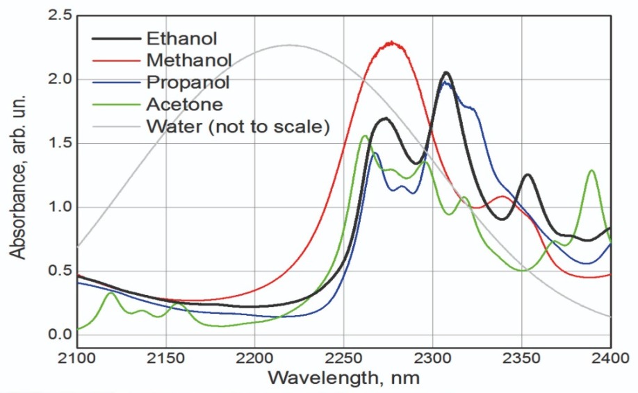
Figure 1. Infrared spectroscopy can identify ethanol, methanol, propanol and acetone by their unique absorbance spectra. The light grey line shows superimposed water transmission spectra.
For high-volume production of infrared and telecom-wavelength optoelectronic devices based on GaAs and InP, the most common substrate size is 3-inch. However, recent developments in datacom technology, primarily the roll-out of low-cost VCSELs, has led to an increase in the use of 6-inch GaAs substrates.

Table II. There are various of light source technology for accessing wavelengths beyond telecom. [1] K. Vizbaras et al. Appl. Phys. Lett. 107 011103 (2015) [2] R. Wang et al. Opt. Express. 24 28977 (2016) [3] R. Wang et al. Sensors 17 1788 2017 [4] S. Sprengel et al. Semicond. Sci. Technol. 31 113005 (2016) [5] K. Vizbaras et al. Proc. Of SPIE 8277 82771B (2012) [6] A. Spott et al. IEEE Photonics Conference 2017, October 10, 2017 [7] M. Razeghi et al. Optics Express 23 8462 (2015) [8] M. Vitiello et al. Optics Express 23 5167 (2015) [9] Cobolt Odin TM, IPG CLT-SF lasers (http://www.ipgphotonics.com/en/products/lasers/mid-ir-hybrid-lasers/1-8-3-4-micron/cl-sf-and-clt-sf-0-2-10-w http://www.coboltlasers.com/wp-content/uploads/2014/11/D0348-B_Datasheet-Cobolt-Odin-Series.pdf ).

Figure 2. The SOI part of Brolis’ widely-swept GaSb/SOI hybrid laser. Two coupled micro-rings are clearly visible.
Figure 3. Superimposed spectra show that four widely-swept GaSb/SOI lasers can cover the spectral range from 1900 nm to 2400 nm. Devices exhibit continuous-wave lasing with output powers of around 1 mW. As tuning involved only tuning a single micro-ring, spectral separation is defined by the free spectral range of a ring (several nm).
Our latest success is the fabrication of a GaSb-based monolithic laser spectrometer, based on four ultra-widely swept hybrid lasers and photodetectors. Lying at the heart of this spectrometer are four single-mode lasers, each with a side-mode suppression ratio exceeding 20 dB. These lasers are combined with two coupled micro-ring resonators with slightly different diameters, realised in an SOI circuit. By turning to the Vernier effect, we are able to electrothermally sweep the laser’s wavelength at a rate of up to 1 kHz. Each laser offers 120 nm of tuning, and by shifting the gain peak for each GaSb light source, we realise a combined tuning range of over 400 nm (see Figure 2).
If we thermally tune just one of the micro-rings, this leads to spectral hopping across the free spectral range of the ring – the mode hops are typically 4-5 nm. By tuning both micro-rings in a coordinated manner, we realise virtually quazi-continuous tuning across the entire spectral range (see Figures 3 and 4).
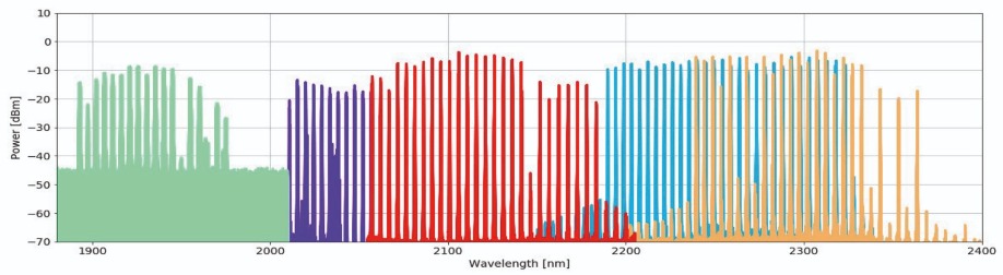
Figure 3. Superimposed spectra show that four widely-swept GaSb/SOI lasers can cover the spectral range from 1900 nm to 2400 nm. Devices exhibit continuous-wave lasing with output powers of around 1 mW. As tuning involved only tuning a single micro-ring, spectral separation is defined by the free spectral range of a ring (several nm).
As one may expect, our first hybrid sensor looked a little ‘clumsy’, as is often the case for new devices (see Figure 5 (a)). But it is functional, thanks to successful integration of four GaSb-based photodetectors, one GaSb-based light emitter and an external SOI cavity. Subsequent miniaturisation of this spectroscopic sensor is in progress (see Figures 5 (b) – 5 (c)), and it includes already 2-4 GaSb gain-chips, butt-coupled to the SOI and 4 GaSb control detectors flip-chipped on the SOI. The experimental tuning range (wavelength map) of one such hybrid device’s one channel is shown in Figure 3. In the long run, the technology should enable a footprint of just 2 x 3 x 1 mm, which is fully compatible with all current consumer and industrial platforms. Current sensor evaluation boards for internal use are shown in Figure 5 (c).

Figure 4. The peak wavelength of Brolis’ single widely-swept laser, when both micro-rings are electrothermally tuned in a specific manner. Continuous spectral coverage is clearly visible.
Multiple markets
The most famous application for spectroscopic sensing is measuring levels of glucose, an insight helping those with diabetes to monitor their condition. Realising this technology is not easy, because sensing glucose comes from measurements made on skin – that is, the tissue matrix – and this has great variability, both from person-to-person and from day-to-day. When those challenges are overcome, there is still the issue that glucose monitoring demands a highly regulated environment. Even if a technology is ready that addresses all these concerns, it could take up to a decade to enter the market.
A related field for transdermal spectroscopic sensors is monitoring lactates. One benefit of keeping track of lactate concentration in human blood is that a rise in value provides an early predictor of sepsis, which is responsible for one in five hospital deaths worldwide.
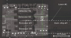

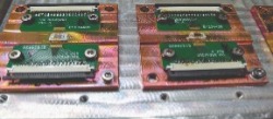
Figure 5. (left) Brolis first integrated GaSb/SOI sensor, based on four widely-swept lasers, has been produced in-house. On the lower right of the GaSb gain chip, the coupled to SOI external cavity is visible, along with: the four GaSb-based photodetectors flip-chipped on the SOI for wavelength control; output power monitoring (centre): and three additional ports for gain-chip coupling (the sides).(middle) Snapshot of current hybrid integration process – two GaSb gain chips butt-coupled to the SOI are visible. The automated hybrid integration robot is Brolis in-house designed and built. (right) Assembled BROLIS sensor demonstrators for evaluation boards (currently for in-house testing only). All four gain-chips, butt-coupled to the SOI are visible.
Another important molecule to consider is ethanol, key to measuring alcohol levels in the blood steam. It is possible to determine levels of ethanol by measuring the reflection spectrum through the skin (see Figure 6). This technique could curb accidents, due to the threat of exposing either drinking and driving, or drinking and working. In addition, it could help everyone to take more personal responsibility, by making self-monitoring available. It is far better to know that you have drunk too much to be safe to work or drive, than to be caught ‘in the act’, possibly after a fatality.
Uptake of a personal alcohol-monitoring system could be very high if such a device could be integrated in a wearable form or added to a wearable/smartwatch platform. Another option, available in the age of the IoT, is to integrate a sensor with a critical piece of machinery, such as a car or industrial tool. This could prevent intoxicated drivers from starting their cars, and operators under the influence of alcohol from using machinery.
Like the measurements of other molecules trans-dermally, it is a challenge to determine levels of ethanol. Success requires a long, expensive research and development effort, so it will be at least three-to-five years before a sensor will enter the market.
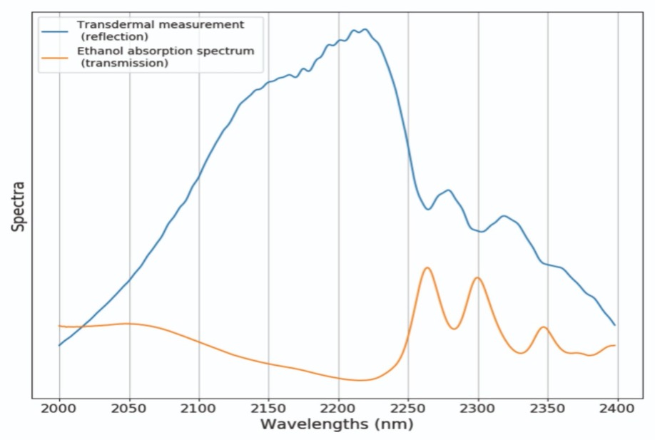
Figure 6. Transdermal optical signal of a tissue matrix containing ethanol, measured in reflection geometry (blue line) and ethanol absorption spectrum (orange). Characteristic ethanol absorption dips are clearly visible in the transdermal signal.
A related opportunity is the deployment of an ethanol content sensor in a fuel or another fluid matrix. This sensor could be handheld, or incorporated into existing industrial machinery.
Yet another potential application for GaSb-based sensors is the sorting of plastics, for recycling or other purposes. Different plastics can be identified by strong, clearly distinguishable features in the spectral range spanning 1.5 µm to 2.5 µm (see Figure 7). A laser spectrometer based on our technology offers a more affordable, compact alternative to the current solution, an expensive short-wave infrared camera.
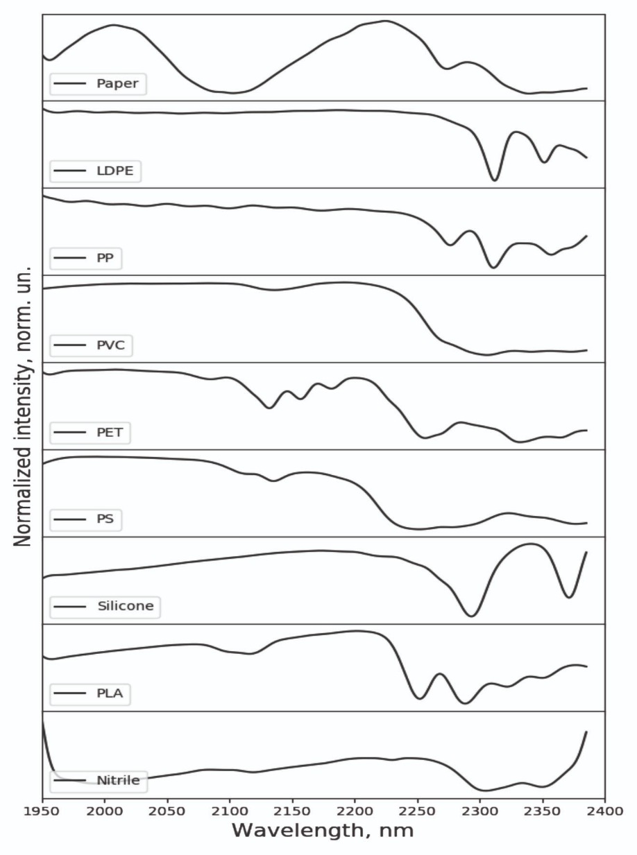
Figure 7. Sorting different types of plastic can draw on the transmission spectra of different materials.
Potentially lucrative opportunities for spectroscopic sensing also exist in the agricultural sector. This technology can identify milk constituents, such as fats, proteins, and urea, because they have significant absorption features between 1.5 µm and 2.5 µm. There is much merit in monitoring milk content in real-time and tracking trends in individual cows and their herds. If farmers monitor and record milk fat, milk protein, somatic cell count and urea content, they can adjust nutrition and get an early warning of incoming mastitis. Armed with this insight, they can take preventative action, rather than eventually prescribing antibiotics and removing the cow from milk production. With our technology, it should be easy to incorporate sensing hardware into most existing milking machinery.

The examples that we have listed here are just a fraction of those that exist for fluid, solid-state and gas sensing. The key point is that our current spectroscopic sensor – that is, our laser-spectrometer that combines widely-swept hybrid GaSb/SOI lasers with an uncooled GaSb-based detector on a single chip – is a powerful, generic piece of hardware that can address niche market segments and be scaled to serve consumer applications.

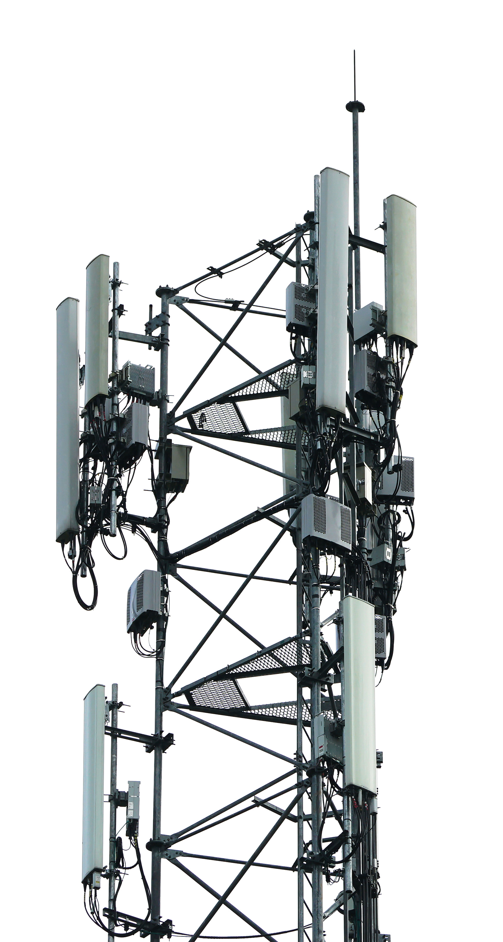
Helping advance the GaN HEMT, researchers are developing processes for manufacturing complex millimetre-wave circuits, getting to the bottom of substrates losses and non-linearities, and speeding p-type devices.
BY RICHARD STEVENSON
RECENTLY, FOR MANY OF US, our mobile has been anything but. Instead, it has sat at home, providing connectivity through our WiFi as we hunker down through wave after wave of the pandemic.
But this time will pass. As the vaccine rolls out, we will return to the outside world and once again rely on networks of base stations to upload web-pages to our phones, and stream music and video. There will be delays in the data at times, and our initial frustration may turn to a desire to see a greater roll-out of a 5G network, to convince us that now is the time to upgrade to a cutting-edge phone.
For 5G infrastructure, GaN is the key material for 5G. When it is used to make solid-state amplifiers, rather than other materials such as silicon and GaAs, it enables higher powers, a high efficiency, and a higher power density. As GaN devices can be built on silicon, high-volume, low-cost production in 300 mm foundries is possible. What’s more, the silicon foundation provides an opportunity to integrate this technology with silicon CMOS. It is a marriage that could aid the development of complex circuits, such as those involving beam-forming and phased-antenna arrays, that are part of the 5G roadmap.
While GaN is by no means the finished article, its weaknesses are being addressed, with significant progress reported at the most recent International Electron Devices Meeting (IEDM), held on-line in late 2020. At that virtual gathering, one imec-led team detailed a 200 mm process for making millimetre-wave GaN on-silicon HEMTs that incorporate three copper layers, another imec-led collaboration reported the results of investigations into substrate RF losses and non-linearities; and a team led by engineers at Cornell University claimed to have obliterated the gigahertz barrier for a p-type GaN HEMT.
Millimetre-wave process
The roll-out of 5G will come in two parts. We are already seeing the introduction of a sub-6 GHz infrastructure that will lead to a slight increase in data rates compared with 4G. Following on, and offering a breath-taking hike in download and upload speeds, will come millimetre-wave connectivity.

Figure 1. Images obtained with high-angle angular dark-field transmission electron microscopy show that the layer of titanium in the metal stack has reacted with AlCu to form TiAl. As TiAl leads to an increase in sheet resistance, titanium has been removed from the metal stack used to make millimetre-wave HEMTs.
“This is probably a technology of choice for sub-6 GHz applications,” claimed Bertrand Parvais, who this December unveiled the latest advances in an on-line talk and accompanying paper. Recent progress has created a second-generation technology, suitable for millimetre-wave circuit operation.
“To achieve this goal, gate lengths have to be scaled down using a 193 nm lithography,” said Parvais. “Furthermore, multi-finger transistors need to be enabled, and this is possible through three layers of copper backend.”
As well as scaling device dimensions and switching from an aluminium back-end-of-line process to one involving three layers of copper, Parvais and co-workers slashed the gate leakage current in their HEMTs, and trimmed the contact and gate resistance.
For the sub-6 GHz technology reported in 2019, imec’s engineers deposited TiN by PVD to form Schottky gates. This led to high-leakage currents, which would exceed the breakdown criteria of 1 mA mm-1 under an off-state bias for gate lengths of 320 nm and below.
To ensure an acceptable gate leakage for a gate length of just 110 nm, which is the dimension employed for millimetre-wave circuits, Parvais and colleagues switched to an ion-metal plasma process for the addition of TiN. This move slashed the leakage current by two orders of magnitude, a breakthrough attributed to the 0.2 eV increase in the work function of TiN.
Shrinking HEMT dimensions can also cause the contact resistance to hamper RF performance. Preventing this from happening, the imec team cut the contact resistance from around 0.3 Ω mm to below 0.15 Ω mm by improving the process for the AlGaN barrier etch and the post-etch clean.
A low gate resistance is key to realising a high maximum-oscillation frequency, essential for millimetre-wave amplification. Accomplishing this with a lift-off process involving a thick gold layer is easy, but that’s not an option, explained Parvais: “In order to ensure CMOS compatibility, lift-off is prohibited, and a gate first approach is adopted in order to avoid any possible degradation during the ohmic contact formation.”
The team from imec deposited a metal stack, before defining the dimensions of the contact with a subtractive process involving lithography and etching. Initially, the stack included a layer of AlCu, sandwiched between titanium. However, intermixing created TiAl (see Figure 1), which has a higher sheet resistance than AlCu. So Parvais and co-workers moved to a titanium-free process that trimmed sheet resistance from 0.55 Ω/square to 0.2 Ω/square. This refinement also increased the maximum oscillation frequency by more than 30 percent.
Fabrication of 110 nm-gate-length HEMTs involved 193 nm lithography and a standard CMOS copper damascene-based process (for more details, see Figure 2).
Measurements on an 8-finger device with a gate length of 110 nm and a total width of 200 mm revealed a drain current of 1.2 A mm-1 at a gate bias of 2 V, and a typical peak conductance of 430 mS mm-1, produced at a drain-source voltage of 4 V. Corresponding values for the cut-off frequency and maximum oscillation frequency were 56 GHz and 135 GHz, respectively.
Large signal characterisation at 28 GHz using HEMTs with a gate length of 200 nm revealed a power-added efficiency of 42 percent at an output power of 17.5 dBm.
Parvais admitted that the cut-off frequency of imec’s HEMT is lower than would be expected for a transistor with a 110 nm gate length. He attributed the shortfall to an issue associated with the patterning of the ohmic layer. Simulations suggest that by addressing this, the cut-off frequency should increase to 80 GHz, along with increases in the maximum oscillation frequency and the power-added efficiency.
RF losses and linearity
One of the weaknesses of the pairing of GaN devices and the silicon foundation is that the finite resistivity of the substrate limits the performance of the transistor, as well as the passives, leading to poor isolation. Employing high-resistivity silicon can help to address this, but the substrate is compromised, with studies showing that losses increase after MOCVD of the HEMT epilayers. Concerns have been directed at: an inversion layer formed at the interface of silicon and the AlN nucleation layer; the creation of S-O-N complexes near the top of the silicon substrate; and diffusion of aluminium and gallium atoms into the substrate, occurring during epitaxy.

Figure 2. Imec’s approach for producing millimetre-wave devices with a three-level copper back-end-of-line process begins with the deposition of a SiO layer and isolation by a nitrogen implant (i). Etching a trench in SiO creates a gate opening (ii), before a further layer of SiO is added, followed by an etch of the source/drain ohmic regions and metallisation, patterning and anneal (iii). The middle-of-line (MOL) includes deposition and planarization of SiO (iv). Vias are then added, by etching the ohmic and gate metals, prior to filling with copper and subsequent chemical mechanical polishing. The M1 dielectric is deposited and patterned, before a copper fill and chemical mechanical polishing. This via and metal process is repeated twice to form the three-copper-layer architecture.
Team spokesman, Sachin Yadav, explained that he and his co-workers used Czochralski silicon for their work, because this is the only substrate available up to 300 mm in diameter. On these boron-doped substrates, which are 1.15 mm-thick, they added a stack of nitride layers by MOCVD to investigate the formation of a parasitic channel, caused by back diffusion of aluminium and gallium atoms during the growth. This diffusion created a p-type layer.

Figure 3. A team from imec considered how the changes to the epitaxial design of the GaN HEMT ((a) to (c)) impact effective resistivity (d) and second- and third-harmonic power ((e) and (f), respectively). The effective resistivity is determined from co-planar waveguides with a centre conductor width of 75 µm and a slot width of 50 µm. Values for the second (H2) and third (H3) harmonic power are measured at a fundamental frequency of 0.9 GHz, and a H1 of 15 dBm, for 1.8 mm-long lines.
Of the three structures grown by the team (see Figure 3), the one with the highest resistivity and greatest non-linearity exhibited the strongest in-diffusion of aluminium and gallium atoms.
One option for providing DC isolation, to make CMOS-compatible GaN HEMTs, is nitrogen implantation. “Our understanding is that implants creates traps inside the nitride layers, which remotely modulate the conductivity of the parasitic surface conduction layer, and hence change the losses,” explained Yadav.
To evaluate the impact of nitrogen implantation, Yadav and co-workers investigated the changes in effective resistivity and second-harmonic power resulting from implants with energies of 75 keV, 150 keV and 375 keV. Any implantation diminished effective resistivity, while the combination of a 75 keV and a 150 keV implant produced the best linearity.
A downside of the silicon substrate grown by the Czochralski process is that it contains interstitial oxygen impurities, stemming from the dissolution of the silicon oxide crucible. If processing steps increase the temperature of this substrate to the range 350°C to 500°C, the interstitial impurities tend to form clusters, which act as electrically active thermal double donors. Such temperatures are common for the fabrication of GaN HEMTs, as they occur during III-V epitaxy, dielectric deposition and ohmic anneals.
Regarding the latter, the formation of low-resistance contacts with a CMOS-compatible process requires rapid thermal annealing between 500°C and 600°C. Yadav and co-workers have considered the impact of this process, finding that a 90 s anneal in nitrogen gas at between 400°C and 600°C degraded effective resistivity. For a high-resistivity silicon substrate with an effective resistivity of 3-6 kΩ cm and an unspecified level of interstitial oxygen, this resistivity exhibited a monotonic reduction with annealing temperature. In contrast, for substrates with effective resistivities of 7.5 kΩ cm and 4.3 kΩ cm and interstitial oxygen levels of 3.8 ppma and 3 ppma, respectively, degradation did not depend on temperature.
Figure 4. Researchers from Cornell and Intel have smashed the gigahertz barrier for p-channel HEMTs with a device with a gate length of just 120 nm. Fabrication of these transistors began with MBE-growth of a GaN/AlN heterostructure with a magnesium-doped In0.05Ga0.95N layer (a). The addition of non-alloyed Pd/Au/Ni ohmics came next (b), followed by a chlorine-based inductively coupled plasma etch for mesa isolation (c), the first recess etch step for removing p-type InGaN (d), a second recess etch with electron-beam lithography to thin the gate-channel distance (e), and the addition of a Mo/Au Schottky T-gate.

Yadav and co-workers have benchmarked their results, considering values for effective resistivity and second-harmonic power. “Our results compare well with many high-res SOI substrate technologies, but still lag the most advanced, trap-rich SOI samples. Further substrate improvements are needed to match that performance.”
Accelerating p-channel HEMTs
Due to challenges associated with p-type doping of GaN, the performance of this class of HEMT has lagged its more common n-type counterpart. If this weakness could be addressed, it would aid development of: wideband amplifiers that handle active loads; the powering of digital-to-analogue converters; and the construction of digital power amplifiers, as this would ease impedance matching and power combining.

Figure 5. A partnership between engineers at Cornell and Intel has propelled the drain current for p-channel HEMTs to a new high. Success results from scaling device dimensions and trimming the contact resistance.
HEMTs were fabricated from GaN/AlN epiwafers, formed by taking Al-polar AlN-on-sapphire templates, loading them into an MBE chamber, and depositing a 500 nm-thick layer of AlN, followed by a 15 nm-thick undoped GaN layer, and a 15 nm-thick heavily doped InGaN layer. This structure forms a two-dimensional hole gas at the GaN/AlN interface, confined in the GaN layer by a valence band offset and a high polarisation field. Devices with a gate length of just 120 nm were formed by mesa isolation, followed by processes including etching and lithography (see Figure 4 for details of the process).
Measurements of the contact resistance showed that this plummets from around 9 Ω mm to below 1 Ω mm when the current exceeds 100 mA mm-1. According to the team, the latter value for the contact resistance is amongst the lowest reported for p-channel HEMTs, and contributes to the high-performance of these devices.
The saturated on-current hit 428 mA/mm at room temperature, for a p-channel HEMT with a source-drain distance of 680 nm. This value breaks new ground for this class of device (see Figure 5).
Even higher values were recorded at cryogenic temperatures. “The on-current almost achieved 1 Amp-per-millimetre at 77 Kelvin,” revealed Nomoto.
High-frequency measurements – involving de-embedding parasitics by using an open structure on the same chip as the p-channel HEMTs – led to values for the cut-off frequency and maximum oscillation frequency of 19.7 GHz and 23.3 GHz, respectively. Compared with conventional HEMTs, source and contact resistances were an order of magnitude higher. Trimming these resistances should lead to even higher frequencies.
The recent breakthroughs made by this team and those led by researchers at imec show that there is much more to come from the GaN transistor. Further advances are sure to be announced at this year’s IEDM, which will hopefully be held in person rather than on-line.


The pandemic is behind soaring sales in some sectors of the compound semiconductor industry, while others take a hit or continue along an existing trajectory
BY RICHARD STEVENSON
We have all suffered from the pandemic on a personal level. Loved ones have been lost, many of us have had to stay at home for weeks on end, and life is not nearly as much fun as it used to be.
However, when it comes to business, it is a very different state of affairs, as we are not sharing in the pain. While millions have been made redundant and countless more had their pay packet cut, some have benefitted from Covid-19. It is well publicised that Jeff Bezos, the owner of Amazon, has nearly doubled his wealth, and some of the providers and distributors of PPE equipment have lined their pockets by applying extortionate margins. Many others that have also done well, growing their investments and swelling their pension funds, thanks to soaring share prices of some companies.
But what about the compound semiconductor industry? Is it a winner, a loser, or a bit of both?
For any manufacturer, the outcome is always influenced by two critical factors. One is the ability to churn out product. Is there a reliable supply of materials? And is the production facility able to run at high capacity? Succeeding on this front is no guarantee of making a profit, however, as financial success also hinges on having strong demand for what is being produced.
Like makers of any class of goods, production facilities within the compound semiconductor industry have suffered from logistical issues, while manufacturing efficiency has been pegged back by the introduction of new practices to minimise transmission of Covid-19. The good news, though, is that the disruption from the pandemic has been fairly minor – it is certainly less than that within the automotive industry, which, for example, saw Tesla’s plants in Shanghai and California shut for a couple of months. Helping chipmakers has been the backing of governments, who are keen to maintain economic activity and view semiconductor production as a critical activity.

Sales of SiC are growing fast, thanks to deployment of these devices in the Tesla 3, X and S models.
Within the semiconductor industry, companies have taken broadly similar approaches. Two of the biggest European players, ST Microelectronics and Infineon, have scaled back production at times – but by not shutting, they have been able to quickly return to normal levels of production. It’s a similar story for the two biggest players in the GaAs RF industry, Qorvo and Skyworks. The latter briefly shut its facility in Mexico, before coming back very quickly, while Qorvo didn’t stop, with the US Government viewing this chipmaker as an essential business.
Increasing sales of SiC power devices are being driven by the electric vehicle industry. Source: Compound Semiconductor Quarterly Market Monitor, Q4, 2020. Module II, Yole Développement.
When it comes to demand, the picture is more complex across the compound semiconductor industry. To understand the impact of the coronavirus, one needs to consider consequences sector by sector. That requires expertise in all areas, from LEDs to lasers, power electronics and RF. Offering such a comprehensive coverage is Yole Développement, which has a team of market analysts covering all the critical bases. They reveal that the consequences of Covid-19 are incredibly varied. The pandemic has had little impact on some sectors, with changes driven by other factors; but this device is also behind some phenomenal successes and depressed sales.
Covid’s silver linings…
One market that has enjoyed a very positive impact from the pandemic is that of LEDs emitting in the UVC domain – that is, wavelengths of 280 nm and below. For more than a decade, UV LEDs have been championed as a great source for disinfection, and this year they have attracted tremendous publicity, as they have been shown to kill Covid-19 bacteria.

Commoditisation of the LED has led to razor-thin margins in the big, established markets of general illumination and backlighting screens. Horticultural lighting, requiring fine-tuning of the emission wavelengths to accelerate plant growth, offers a more lucrative opportunity.
Pars Mukish, the Market and Technology Analyst in the field of LED at Yole, told Compound Semiconductor that he is expecting the UVC LED market to have nearly doubled between 2019 and 2020, climbing from $144 million to $308 million. From this year onwards, growth will slow, to a still very healthy compound annual growth rate of 52 percent through to 2025. By then the sector will be worth $2.5 billion.
“Those figures take into account the development of a vaccine,” says Mukish, who explains that the epidemic has provided a tremendous spark for the UVC LED industry. Last year’s jump in sales came on the back of steady progress throughout the last decade, with improvements including a staggering reduction in the cost-per-Watt – this tumbled from nearly $100 per milliwatt in 2015 to around just $1 per milliwatt by the end of last year.
Lamps based on the UVC LED are also undergoing a rapid rise in sales. One example of this is global lighting manufacturer Signify, formerly Philips lighting. Revenue for its UV lamp business grew by 73 percent between 2019 and 2020, and last June it announced plans for an eight-fold increase in production capacity.
Note that the UVA LED industry, which provides sources for curing adhesives, is not on the same trajectory. Mukish explains that as UVC LEDs emit at wavelengths only a little shorter than their visible counterparts, makers of blue LEDs have flooded this market, driving down prices. Note that those chipmakers are not able to move further in this direction and target the UVC LED, because it has a markedly different, more complex architecture.
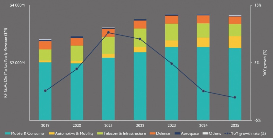
Despite a substantial fall in handset shipments in the first half of 2020, revenue for GaAs die continues to climb, thanks to the rollout of 5G and a move to the Wi-Fi 6 standard. Source: Compound Semiconductor Quarterly Market Monitor, Q4, 2020. Module II, Yole Développement.
One would expect the makers of InP edge-emitting lasers used in metro and long-haul networks, along with the manufacturers of GaAs VCSELs that are employed in data centres, to have benefitted from the epidemic. With internet traffic reaching a new high, now that many of us spend much of our working day on video calls, there is much demand to increase network capacity. However, Mukish believes that this pressure will not have an immediate impact. Instead, it will take time to strengthen infrastructure, which will help to accelerate the digitalisation of our world.
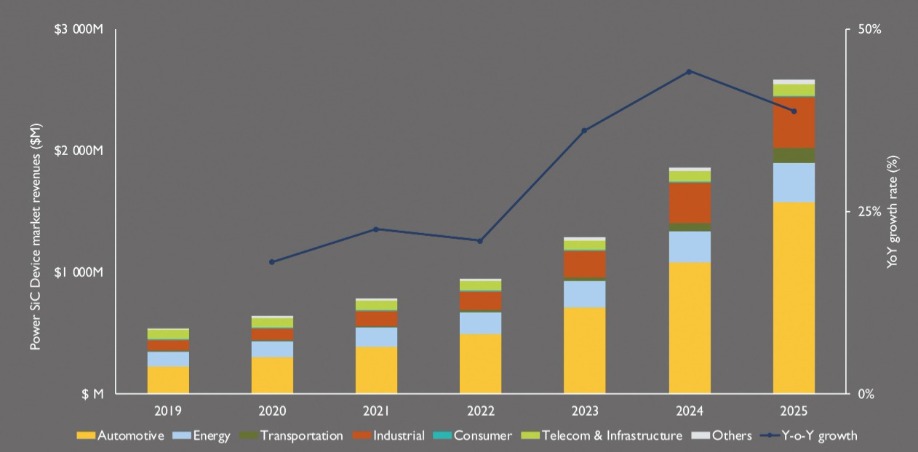
What may raise a few eyebrows is the positive impact that Covid is having on the SiC market. After all, the outbreak of this virus chocked car sales. However, the response from governments all around the world has been to try and support this industry by helping speed its electrification – China has plans to extend subsidies for this sector to 2022, while citizens of Germany, France, Spain and the UK are being offered financial incentives to go out and buy electric vehicles. This is great news for the SiC sector, with sales to the electric vehicle industry forecast to grow and account for a 60 percent share by 2025, according to Yole Développement.

Revenue for the GaN power device market is taking off, thanks to the rapid growth of 65 W fast chargers incorporating this technology. Source: Compound Semiconductor Quarterly Market Monitor, Q4, 2020. Module I, Yole Développement
Yole’s Ezgi Dogmus, Technology and Market Analyst, Compound Semiconductors, says that the deployment of SiC in electric vehicles has started with high-end cars, such as those made by Tesla. Elon Musk’s company deploys this material in its Model 3, S and X. “We are aware of other OEMs that are coming with SiC adoption this year,” adds Dogmus.
When Tesla started adopting SiC in its vehicles a few years’ ago, the corresponding hike in orders for power devices led to concerns over SiC substrate supply. Leading chipmakers ensured that they would not miss out by negotiating supply contracts with the biggest producer of SiC substrates, Wolfspeed. Since then supply concerns have fallen, according to Dogmus, who says that the market is now benefiting from more suppliers, including Chinese firms Tanka Blue and SICC, who have big expansion plans.
As well as the increase in the number of producers of SiC substrates, chipmakers are benefitting from the introduction of SiC crystals on the market, provided by US firm GTAT. Dogmus says that GTAT established a partnership with ON Semiconductor, and has more recently entered into another with Infineon. “This is an interesting approach for companies who have internal SiC wafering facility, which can help them to grow and produce their own wafers, and also reduce their SiC dependence on other external factors.”
and grey clouds
Within the automotive industry, investment in electrification has come at the expense of LiDAR, which has seen projects associated with this technology delayed. However, although this will hamper sales of edge-emitting lasers, it will not have a significant impact, says Mukish: “When you take a look at the LiDAR market it’s quite huge, and there are not so many automotive brands that are implementing it.”

65 W fast chargers based on GaN devices are driving rapid growth in the GaN power electronic market. Source: Compound Semiconductor Quarterly Market Monitor, Q4, 2020. Module I, Yole Développement.
The smartphone market has suffered from shuttered stops, travel restrictions and a tightening of belts. Global shipments for 2020 were down compared with 2019, particularly in the first two quarters.
For makers of VCSELs, a fall in smartphone sales is only part of the problem. There has also been a shift from using a pair of front-facing VCSELs in facial recognition systems, to a single world-facing emitter for photography or augmented reality. “There will be a direct impact on the volume of VCSELs and the revenue,” says Mukish, adding that Yole has revised down its forecast accordingly. However, despite this headwind, the VCSEL market is still expected climb at a compound annual growth rate of 18.4 percent until 2025, to total $2.7 billion.
Dominating VCSEL sales is Lumentum, which sources its epiwafers from IQE. Lumentum enjoyed a 49 percent share of the market in 2019, aided by contracts with Apple, which has generated the highest volume for VCSELs for 3D sensing. However, Apple is diversifying its supply, with a significant and growing number of VCSELs coming from II-VI, thanks to its acquisition of Finisar in late 2019.
Despite a reduction in smartphone shipments in 2020, revenue for GaAs microelectronics increased year-on-year, according to Yole’s Poshun Liu, a Technology and Market Analyst, Compound Semiconductors and Emerging Substrates. He argues that this rise in global sales is due to the need for the latest phones to incorporate power amplifiers for both 5G and the new Wi-Fi protocol, Wi-Fi 6. Going hand-in-hand with the higher revenues are increases in the volume of both GaAs chips, and their associated epiwafers.
“5G and Wi-Fi 6 – Wi-Fi is a big selling point – are driving the replacement of the new phones for consumers,” says Liu, pointing out that many OEMs have recently released models featuring these technologies. Looking further ahead, 5G phones will start to include amplifiers operating in the millimetre-wave, further increasing volumes for GaAs microelectronic devices.
Yole’s last forecast for the visible LED market came out in 2019, when analysts predicted sales of $17.4 billion for that year and a modest compound annual growth rate out to 2024 of 5 percent. Figures from TrendForce released in late 2020 suggest that the pandemic has taken its toll on this sector – declines in commercial lighting, outdoor landscape lighting, and outdoor displays have outweighed gains in sales for backlighting TVs, tablets and laptops. Total revenue is tipped to fall by 10 percent between 2019 and 2020, before showing a slight increase in 2021.
Even before the pandemic, the visible LED market was in the doldrums, according to Mukish. “General lighting, initially the killer application for the LED, ended up being a bloodbath after the entry of Taiwanese and Chinese players that created a situation of overcapacity and strong price pressure.” It is this state of affairs, rather than any consequence of Covid, that led Cree/Wolfspeed to sell off the LED-based parts of its business, and focus on RF and power electronics.
Commoditisation of the LED industry is not going to be accelerated by the pandemic. “It’s already commoditised,” argues Mukish, who believes the pandemic could drive further consolidation of this industry.
To secure better margins, some of today’s leading LED manufacturers are targeting two niche areas: exterior automotive lighting and horticulture.
LED-based headlamps continue to evolve, now offering an opportunity for carmakers to enhance their brand by making it instantly recognisable in the dark. One of the latest advancements is to combine brand-specific lighting with a camera, to create a smart headlamp offering controllability, such as the direction of the beam. “Only a few companies can supply those kinds of device, mostly for headlamps, because this is where you require really high power, and really high power-density devices, which means expertise in thermal management and so on,” explains Mukish. He says that Osram is the key supplier for automotive lighting, a niche that also brings in revenue for Lumileds.
The latter is a key player in horticultural lighting, where success hinges on fine-tuning emission wavelengths rather than optimising power density. Scientists are just starting to discover the optimal spectra for accelerating growth of specific plants, fruit and vegetables.
Independent success
One rapidly growing market that is not deriving any benefit from the epidemic is GaN power electronics. Chips are being deployed in fast chargers for mobile phones. Sales are ramping so fast that the GaN power market almost doubled between 2019 and 2020.
Yole’s Ahmed Ben Slimane, Technology and Market Analyst, Compound Semiconductor and Emerging Substrates, told Compound Semiconductor that sales of GaN power devices began to take off in late 2019, when Reno’s Ace Oppo Phone started to be dispatched with an accompanying 65 W GaN charger.
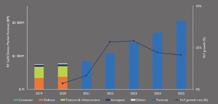
Tensions between the US and China are impeding the growth of the GaN RF market. Source: Compound Semiconductor Quarterly Market Monitor, Q4, 2020. Module II, Yole Développement.
“We have identified two main companies that have targeted this consumer market: Power Integration and Navitas,” says Slimane. “They both have products and design wins with different Chinese OEMs, and other OEMs.” Due to this activity, several models of smartphone now come with a GaN charger.
Rapidly growing markets always attract competition. Slimane says that Transphorm, GaN Systems and EPIC have all released impressive performance figures for their products that will help them to enter the GaN fast-charger market, which is also going to be targeted by big IDMs, such as STMicroelectronics and Texas Instruments.
Like the GaN market, that for microLEDs has not been impacted by Covid-19. For microLEDs, that’s because the market is emerging. It did reach an important milestone last year, with the release of the first commercial product.
According to Mukish, the next steps for this sector are further development of the technology, and the release of a “real” consumer product. “I say a real consumer product, because when you take a look at the product from Samsung, it’s a luxury TV with a price tag of nearly $150,000,” explains Mukish. While such an expensive item is out of the reach of most of us, prices may not need to tumble as much as one might expect before a trickle of sales begin, thanks to the emergence of a luxury, high-end TV market.
Trade wars
For the makers of RF GaN devices, the two largest markets are defence and telecom infrastructure. RF GaN is already established in wireless infrastructure, having been used in 4G LTE base stations. GaN is the preferred technology for Huawei, which is deploying 5G infrastructure in China, and for European rivals Nokia and Ericsson.
According to Slimane, the pandemic has not had a big impact on the RF GaN market for 5G. What has held back sales is an ongoing trade war between the US and China, with Huawei impacted severely by restrictions, which have also dragged down revenue for Skyworks and Qorvo.
“2021 will be an important year to watch,” says Slimane. “There will be a new presidency, and this might bring a new strategy with China.”
Once Joe Biden takes over, there will also be a dramatic shift in the position of the US towards climate change, possibly providing another boost to the makers of electric vehicles and those in this supply chain. Another big change this year will be the wide roll-out of an effective vaccine, which will help to ensure smooth running of all compound semiconductor fabs. As the analysis by Yole shows, our industry has not taken any major blows from the pandemic, and a trajectory of long-term growth looks set to continue throughout this decade.
Inserting quantum dots in nanopores creates efficient, reliable microLEDs.
BY JIE SONG AND CHEN CHEN FROM SAPHLUX
DISPLAYS MADE from microLEDs are attracting tremendous attention due to their long lifetime, high brightness and excellent efficiency. Helping to put them in the spotlight are some of the biggest tech companies in the world, such as Apple and Samsung, which are developing this form of display using mass-transfer or nanoprint technology.
Despite years of intense development, several key technical issues are still hampering the key ingredient, the miniaturised LED. Those emitting in the red are plagued by a low efficiency and a thermal droop, limiting the performance of the display; it is challenging to fabricate devices with a pitch below 10 µm, a requirement for microdisplays for augmented reality and mixed reality; as the size of the LED reduces, bin sorting gets harder and more costly; and of greatest concern of all, production costs are high.
Helping to address all these issues are colour-converted microLEDs, which use a chip emitting in the ultraviolet or blue part of the spectrum to pump quantum dots. Devices that operate in this manner have many unique properties, including a high quantum yield, a size-dependent emission wavelength, a narrow emission linewidth, and a short luminescent lifetime. What’s more, by using patterning and spin-coating to add quantum dots to the substrate, this class of LED can serve a broad range of applications.
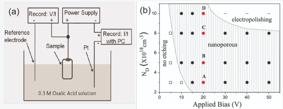
Figure 1. (a) An electrochemical etching process produces nano-porous GaN. (b) A phase diagram of the GaN electrochemical etching process shows how the etching characteristics are related to silicon doping in GaN and the applied bias.
To address these issues, our team from Saphlux of Branford, Connecticut, has developed a nano-pore technology that allows quantum dots to be embedded in microLEDs. This results in devices that are very efficient, reliable, and low in cost.
Nano-porous GaN
We create nanoscale pores in our LEDs by dipping the material in an acidic solution and applying a bias, which drives electro-chemical etching of n-type GaN (see Figure 1 (a)). By varying either the applied bias voltage or the silicon doping concentration in GaN, we are capable of producing dramatic changes in electro-chemical etching behaviour. If we apply a low bias voltage to GaN with a low silicon-doping concentration there is no etching; and if we use a high bias voltage or a high silicon-doping concentration, we etch GaN completely away (this is called electropolishing). To form nano-porous GaN we chart a course between these extremes, selecting an appropriate bias voltage and silicon doping concentration.
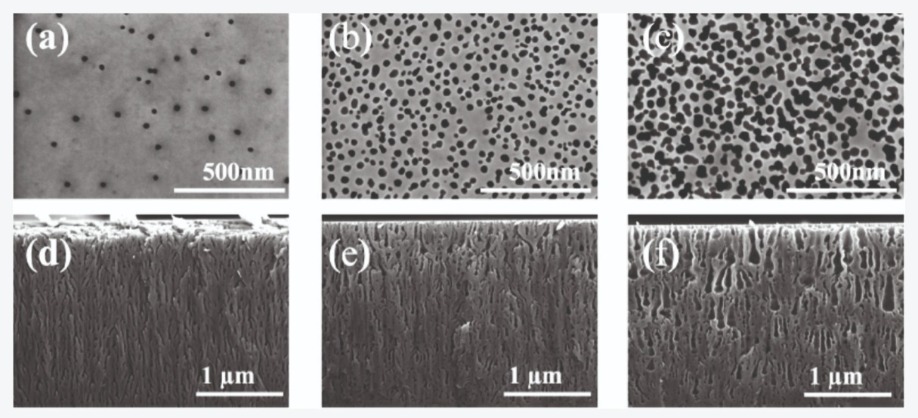
Figure 2. (a-c) Top-view and (d-f) cross-sectional scanning-electron microscopy images of nano-porous GaN with different porosity etched at different bias voltages. Reprinted with the permission of the American Society Chemistry.
Simulations suggest that the incorporation of nanopores into our LEDs can lead to a tremendous increase in device efficiency. For planar quantum dots in a polymer film, light-conversion efficiency increases linearly with increases in the thickness of the quantum dot layer to a maximum of only 20 percent – that’s for a 10 µm-thick quantum-dot layer (see Figure 3(a)). In stark contrast, when dots fill the nanopores, light-conversion efficiency exceeds 80 percent, for a film thickness of just 5 µm.
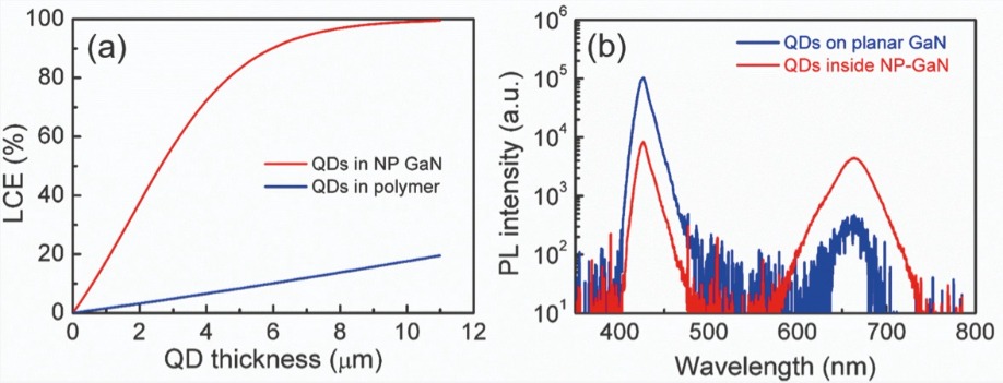
Figure 3. (a) Simulated results for the light-conversion efficiency (LCE) of quantum dots (QDs) loaded in polymer and nano-porous GaN, respectively. The same concentration of dots is used in both samples. (b) Photo-luminescence spectra of red QDs on planar GaN and nano-porous GaN, respectively.
Benefits of the nano-porous structure are not limited to greater efficiency. Reliability also increases, as demonstrated by our optical excitation measurements at a high power density. When we pumped the planar samples with a 420 nm blue laser at an optical power density of about 25 W cm-2, the normalized intensity of red emission fell to just 20 percent of its initial value after 3 hours of excitation. In comparison, when dots were housed in the nano-pores, identical excitation conditions led to a 55 percent reduction in intensity compared with the initial value.
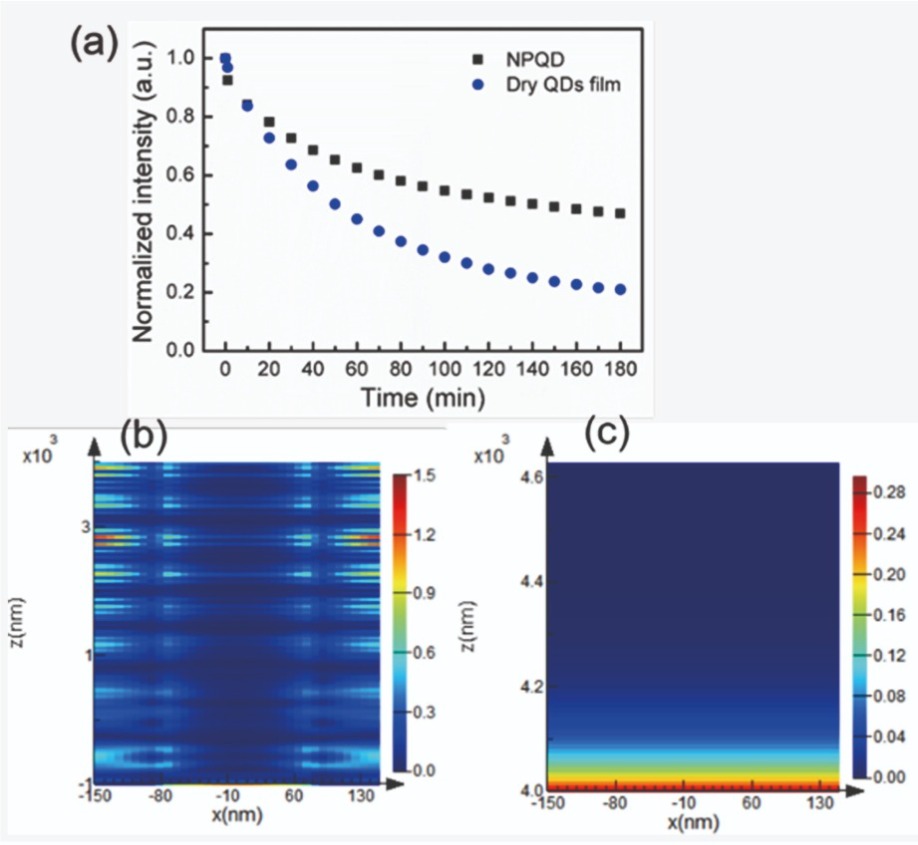
Figure 4. (a) Comparison of the normalized power intensity of red emission from a red nano-porous quantum-dot sample and a quantum-dot film on a GaN-on-sapphire wafer. Both samples were subjected to 3 hours of excitation with a 420 nm blue laser. (b) Simulated mapping results of blue light absorption by nano-porous GaN. (c) Simulated mapping results of blue light absorption by a nano-porous film.
Dots for displays
Producing our displays involves forming nano-porous blue-emitting LEDs, before putting some of them aside and coating others with either red-emitting or green-emitting dots (see Figure 5). We bond exposed nano-porous GaN to a current driver panel, before loading red- and green-emitting dots onto different zones. If the zones are free from dots, they emit blue light; and if they are loaded with dots, they produce red or green emission through colour-conversion.
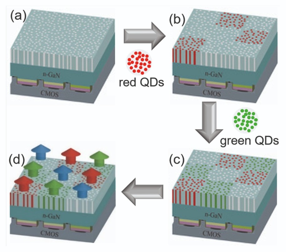
Figure 5. Saphlux’s approach to making monolithic RGB microLEDs. (a) A vertical blue LED with exposed nano-porous GaN is bonded to a current-driver panel. (b) Red quantum dots are selectively loaded into red zones. (c) Green quantum dots are selectively loaded into green zones. (d) Red, green and blue light emitted from red quantum dot zones, green quantum dots zones, and zones without any quantum dots, respectively.
We are now fabricating nano-porous GaN microLED arrays with customized pixel sizes to suit the needs of our customers. Many applications offer broad market prospects, including wearable devices, vehicle displays, smartphones, and various forms of augmented and virtual reality.
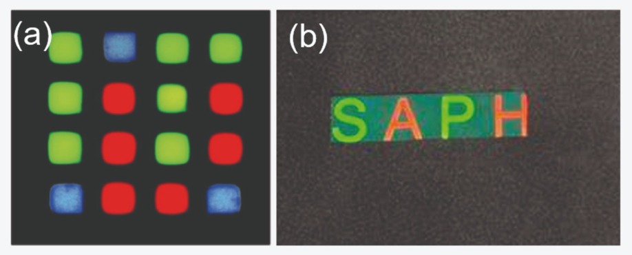
Figure 6. (a) Saphlux RGB monolithic microLEDs excited by a blue LED source from the backside. (b) A picture of the company logo “SAPHLUX” fabricated by red and green nano-porous quantum-dot microLEDs.
These devices, like their smaller siblings, show much promise. They are well-positioned to drive the manufacture of displays made from tiny, efficient, reliable LEDs that are low in cost and will help this market to blossom.
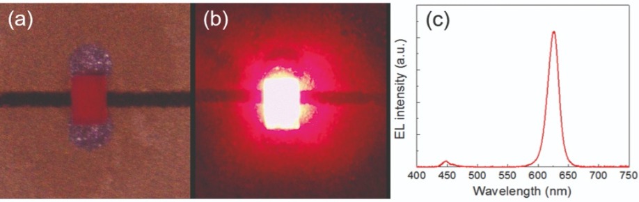
Figure 7. Photos of 100 × 150 µm2 red nano-porous quantum dot miniLED mounted on a PCB board (a) and lit-up at an injection current of 1 mA (b). (c) Spectrum of a red nano-porous quantum dot LED shown in (b). Testing the reliability of the red nano-porous quantum-dot miniLED revealed acceptable results at 30 W cm-2. This power density is more than sufficient for most microLED applications.
D. Peng et al. J. Disp. Technol. 12 742 (2016)
H.-V. Han et al. Opt. Express 23 32504 (2015)
J.-H. Kang et al. ACS Appl. Mater. Interfaces 12 30890 (2020)
C.-T. Lee Cheng et al. IEEE Photonics Technol. Lett. 27 2296 (2015)
K.-B. Bae Lee et al. Phys. Status Solidi A 215 1700644 (2018)
E. Jang et al. Adv. Mater. 22 3076 (2010)
Nanowire lasers could provide the telecom industry with a widely tuneable source that is easy to integrate with silicon photonics.
BY GUOQIANG ZHANG FROM NTT CORPORATION
ALMOST ALL DEVICES produced by our industry are formed from compound semiconductor heterostructures. By controlling the composition, doping and thickness of every layer within an epitaxial structure, we are able to produce a wide range of devices with excellent characteristics.
One such device is the edge-emitting InP-based laser. Generating sales of billions of dollars, this class of laser, which operates in the spectral domain spanning 1.2 µm to 1.6 µm, is a key ingredient in optical communication networks.
To produce these telecom lasers, engineers load InP substrates into MOCVD reactors and deposit an epitaxial stack containing layers of InP and InGaAs(P). It is a material combination that has its pros and cons – by adjusting the composition, the designer can adjust the wavelength of the laser’s emission, targeting absorption minima in optical fibres; but there are mismatches in lattice and thermal expansion coefficient between InP and its related alloys, and this hampers further integration into functional systems and platforms.
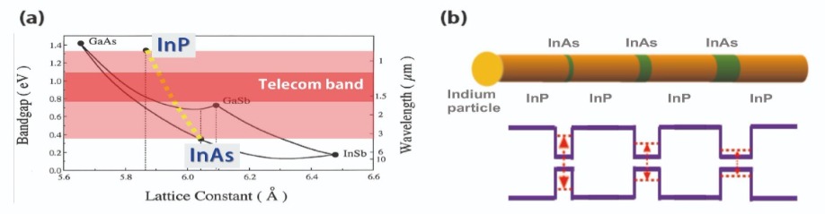
Figure 1. (a) Bandgap and lattice constant of III-V compound semiconductors. InP/InAs can cover a wide spectral range, including the telecom band. (b) Lattice-matching constraints are far less severe in InP/InAs heterostructure nanowires connected by a single indium particle, than in conventional heterostructures. In these nanowires, the quantum confinement effect along the axial direction allows the real bandgap of the InAs layer to be modulated by the thickness.
By targeting the 1.2 µm to 1.6 µm domain with our nanowire lasers, as well as providing potential sources for data transmission through fibre, we have the opportunity to turn to mature silicon photonics platforms for integration – that’s because silicon is transparent at telecom wavelengths.
We form our telecom-band single-nanowire lasers from InP/InAs quantum heterostructure nanowires. The pairing of InP and InAs can create quantum heterostructures with a wide spectral range that includes the telecom band, thanks to a substantial quantum confinement in an InAs quantum disc along the axial direction (see Figure 1).
Mastering mismatch
In planar structures, growing InAs layers on InP tends to result in a high density of dislocations in the InAs active layers, due to significant lattice mismatch – it is 3.1 percent (see Figures 2 (a)-(c)). This mismatch makes it extremely challenging to form dislocation-free InAs active layers with excellent optical properties.
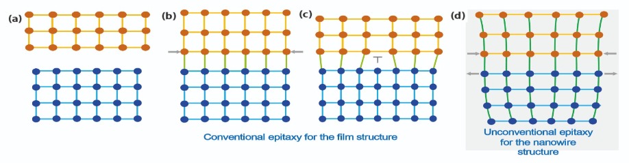
Figure 2. Strain relaxation for crystal materials with lattice mismatch varies between conventional heterostructures and nanowires. (a) Lattices of crystalline materials before epitaxy. (b) Coherent growth by elastic deformation of the epi-layer lattice. (c) Incoherent growth (strain relaxation by mismatch dislocations). (d) Coherent growth by elastic deformation of both lattices. In contrast to the film structure, the lattice in the nanowire structure can deform much more along the radial direction because of its microscale or nanoscale diameter. Thanks to this, nanowires can endure higher strain induced by lattice mismatch.
Researchers have used gold-particle-catalysed vapour-liquid-solid growth to fabricate various nanowires, including those based on GaAs and InP. Using gold is not ideal, because it is incompatible with the mainstream CMOS process and consequently hinders integration of optically active III-V nanowires with silicon technology. Far better alternatives for producing compound semiconductor nanowires by the vapour-liquid-solid growth approach are particle catalysts based on either group III or V elements – and out of these two the former is more suitable.
Figure 3. Schematic diagram of the vapour-liquid-solid growth mode. InAs and InP nanowires can be grown by the self-catalysed vapour-liquid-solid mode using indium particles.
The high quality of our structures is evident in high-angle annular dark-field scanning transmission electron microscopy, which reveals the multiple quantum disc layers along the [011] direction (see Figure 4 (c)). Our structures result from a vapour-liquid-solid growth mode that is dominant along the axial direction. Thanks to the low growth temperature, negligible growth occurs in the radial direction via the conventional film growth mode – this is the uncatalyzed mode. With all these factors at play, there is high growth controllability, ensuring homogeneity of the gain medium throughout the entire multiple quantum disc region.
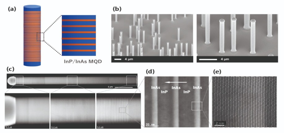
Figure 4. InP/InAs multi-quantum-disc (MQD) nanowires. (a) Schematic diagram of a MQD heterostructure nanowire and a magnified view of the heterostructure highlighting the InP/InAs MQD structure. The InAs layer is indicated in red. (b) Scanning electron microscopy images (tilt: 38º) of InP/InAs MQD nanowires grown on an InP (111)B substrate. (c) High-angle annular dark-field scanning transmission electron microscopy (HAADF-STEM) images of an InP/InAs MQD nanowire taken along the [011] zone axis. The nanowire contains 400 units of InP/InAs heterostructure. ((d) and (e)) Aberration-corrected HAADF-STEM images of InP/InAs heterostructures taken along the [011] zone axis. The horizontal white arrow indicates the growth direction. The thicknesses of the InAs layer and the InP barrier layer are 9.0±1 nm and 25.6±1 nm, respectively.
Creating cavities
We turned to micro-photoluminescence to characterise the optical properties of our nanowires. When they are mechanically dispersed onto foreign substrates, we can remove the indium particles at their tips to create a (111)-facet mirror – and thus a Fabry-Pérot cavity. This structure has intrinsic Fabry-Pérot resonance modes with a sufficiently large mode index in a wide diameter range.
Optically pumping our nanowires leads to lasing behaviour. Measuring the photoluminescence of numerous individual nanowires reveals a broad spontaneous emission spectrum, with a peak wavelength around 1.57 µm to 1.59 µm. When pumped with an excitation power of 2.15 mJ cm-2, a spike centred at 1573 nm appears. Plotting the light input-output curve by varying the excitation power uncovers a strong transition from spontaneous to stimulated emission.
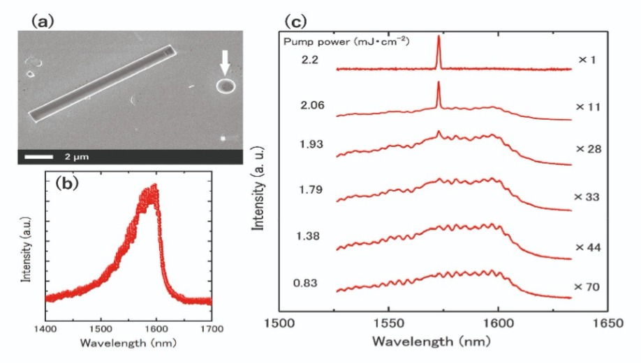
Figure 5. (a) Scanning electron microscopy image of a nanowire mechanically dispersed onto a gold-film-covered SiO2-on-silicon substrate. The white arrow indicates a removed indium particle. (b) Photoluminescence spectrum of a single nanowire under a pump laser power of 0.83 mJ cm-2. (c) Photoluminescence spectra of the nanowire with increasing pump power, revealing spectral narrowing.
So far, we have described optically pumped devices. However, many applications, including photonic integration, demand current-injection light emitters. It is incredibly challenging to realise current-injection lasing from single nanowires, because making a direct electrical contact to them deteriorates light confinement. However, we have taken important steps towards this goal, demonstrating LEDs with p-i-n-structured nanowires that emit in the telecom range.
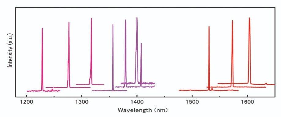
Figure 6. Nanowires allow a tuning of the laser wavelength range in the telecom band. Spectra are offset for clarity. The laser wavelength is modulated by the growth parameters, such as flow rates of the metal-organic sources. Thus a broad wavelength range is covered in the whole telecom band, including the two technologically important telecom-band windows centred around 1.3 µm and 1.55 µm.
To form our novel LEDs, we began by embedding these nanowires in transparent insulating benzocyclobutene. Subsequent reactive-ion etching then removed this organic from the surface, exposed the nanowire tips, and ultimately paved the way to adding electrical contacts. Depositing AuZn metal onto the p-InP substrate and indium-tin-oxide onto the n-InP nanowire segment created electrical contacts for this device.
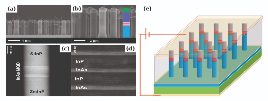
Figure 7. Morphological and structural analysis of InP/InAs heterostructure nanowires. (a) and (b) Cross-sectional scanning electron microscopy images of InP/InAs nanowires. The inset shows the p-i-n structure of these nanowires. (c) and (d), high-angle annular dark-field scanning transmission electron microscopy images of the multi-quantum-disc (MQD) active region between zinc-doped and sulphur-doped InP segments. The MQD active region consisting of 10 InAs quantum discs. (e) A diagram of the nanowire LED device. (Figure reprinted with permission from IOP publishing).
Critical to the development of high-performance optoelectronic devices is tunability of the electroluminescence wavelength. Our multiple quantum disc active region allows us to modulate the photon emission energy by adjusting the thickness of single InAs quantum discs – this alters the quantum confinement along the axial direction. Thanks to the high degree of control provided by vapour-liquid-solid synthesis, we are able to precisely define the thickness of each InAs quantum disc, and thus tune the electroluminescence in the O and E bands of the telecom range.
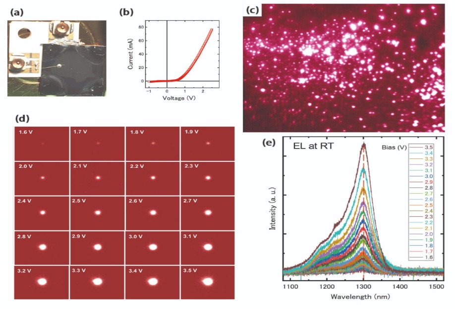
Figure 8. Electrical performance of a nanowire LED at room temperature. (a) The nanowire sample is fixed to a white ceramic substrate with metallic electrodes. The black-colour area is the nanowire LED device (10 µm ×10 µm). (b) A typical current-voltage curve for a nanowire LED. (c) An electroluminescence image taken by an infrared camera under an LED bias of 2.5 V. (d) Electroluminescence images of a single luminescent nanowire with increasing bias (step: 0.1 V). The area of each image is 24 µm × 36 µm. (e) The electroluminescence spectra of the nanowire shown in (d) with increasing bias (step: 0.1 V). The spectra show a constant peak at 1300 ± 5 nm, corresponding to the O-band of telecom-band range. (Figure reprinted with permission from IOP publishing).
G. Zhang et al. ACS Nano 9 10580 (2015)
G. Zhang et al. Nanotechnology 29 155202 (2018)
G. Zhang et al. Sci. Adv. 5 eaat8896 (2019)
H. Sumikura et al. Nano Lett. 19 8059 (2019)
G. Zhang et al. Jpn. J. Appl. Phys 59 105003 (2020)

GaN HEMTs operating at voltages of up to 150 V outperform vacuum tubes by combining high performance with greater reliability, longer lifetime and lower operating costs
BY GABRIELE FORMICONE, JEFF BURGER, JAMES CUSTER AND JOHN WALKER FROM INTEGRA TECHNOLOGIES
INVENTED PREDOMINANTLY in the first half of the twentieth century, vacuum electron devices (VEDs) have a long history as a critical component enabling satellite communications, radar systems, high-energy particle accelerators, and other applications requiring high output power, wide operating bandwidth and high efficiency. VEDs include traveling-wave tubes and klystrons.
While VEDs are an accepted technology, they suffer from multiple weaknesses, many of which can be addressed by semiconductor-based solid-state amplifiers, which have become the mainstream technology in the lower power, lower frequency VED market. Semiconductor-based solutions deliver longer lifetime, superior ruggedness, and higher reliability, and reduce overall system size, weight, and costs. Yet despite all this success, solid-state sources have yet to penetrate the high end of the market for high power, multi-kilowatt applications.
Modernization of high-power RF communication and data transmission systems will push the requirements of what traditional VEDs can deliver. In addition, system architects are demanding more efficient power sources to meet green requirements while driving down operating costs over the system life. Thanks to the pioneering work of our team at Integra Technologies Inc., a market leader in RF and microwave high power devices, we have achieved a breakthrough by pushing the operating voltage for this class of device to a new high, raising the bar for high efficiency GaN-on-SiC technology. These efforts draw on our long heritage of silicon bipolar and GaN/SiC RF high power expertise at 28 V and 50 V, with our latest success representing yet another milestone in our advancements in green technology, which date back to 2013. The ground-breaking progress that we have made enables high-voltage GaN/SiC-based HEMTs to offer a compelling commercial alternative to the VED.

Figure 1. Measured RF power gain and drain efficiency versus output power at 145 V bias and 400.8 MHz. Quiescent current is 100 mA. 6 Ω series gate resistors help to stabilise the transistor with 20 dB gain at 2 dB compression and 2.3 kW saturated power. Drain efficiency peaks at 80 percent. In CW operation at 100 V bias, saturated power is 1.2 kW with the same 80 percent peak drain efficiency.
Leveraging this field-proven IP, we have developed new epitaxial structures specifically designed for high-voltage operation. In addition to this advance, we have introduced and then patented innovated circuit and thermal management techniques specifically for high power operation. Benefiting from all this progress, our devices can now operate at voltages of up to 150 V, resulting in a dramatic improvement in output characteristics.
Our latest generation of high-voltage GaN/SiC devices, which produce pulsed power densities up to more than 20 W/mm, enables the production of solid-state devices with an output power of several kilowatts. Critical to the performance of the next high-power-generation green platforms, our HEMTs deliver sufficient gain, efficiency, and reliability to enable these systems to fulfil their performance targets.
Our devices are manufactured in a mainstream wafer fabrication foundry, using commercially available, production-ready materials.
Increasing power and dynamic range
At last year’s International Microwave Symposium, our company demonstrated the incredibly high output powers that can be produced by RF GaN/SiC transistors operating at elevated voltages of between 100 V and 150 V. We reported 2 x 50 mm gate periphery die yielding 1.2 kW when operating in CW mode at 100 V, and producing 2.3 kW when driven at 145 V using 100 µs-wide pulses and a 5 percent duty cycle. Plots of power gain and drain efficiency versus output power for these devices, which have a drain efficiency of 80 percent when operating in both modes, are shown in Figure 1. Two key features of this amplifier’s design are harmonic tuning, used to realise high efficiency, and patented thermal enhancement techniques that help mitigate heat dissipation in such high-power density transistors. We have designed the devices and circuits to operate at 400.8 MHz. This is the frequency employed in today’s largest particle accelerators, and also a frequency of interest for long-range, early-warning radar systems.
Our technology enables a single transistor to produce a CW power level of 2 kW and a pulsed output of 4 kW at an efficiency greater than 70 percent. With this level of performance, megawatt power levels can be realised with fewer combiners and lower related losses. By comparison, off-the-shelf 50 V RF technology would require massive power combiners to achieve similar performance, degrading system efficiency, while increasing the complexity of heat extraction. We also showcased the design flexibility of this technology by increasing the operating voltage to 150 V at the 2020 European Microwave Week. In this forum, we reported a single 50 mm gate periphery die that produced a 3 dB power dynamic range when modulating its operating bias from 100 V to 125 V and then on to 145 V (see Figure 2).
This amplifier’s devices and circuits are designed to operate at 325 MHz, targeting large particle accelerators. Our single semiconductor die delivers a 1.1 kW peak power at 145 V with 80 percent peak efficiency. The peak power decreases by about 3 dB at 100 V bias.
Going to even lower voltages can offer additional benefits. When we dial back the bias to 50 V, peak power can be modulated by around 6 dB while still preserving 80 percent peak efficiency; and we can realise additional dB of dynamic range by reducing the operating bias towards 28 V or 32 V. We have obtained similar results, also announced at European Microwave Week, with a power amplifier designed to operate at 650 MHz.
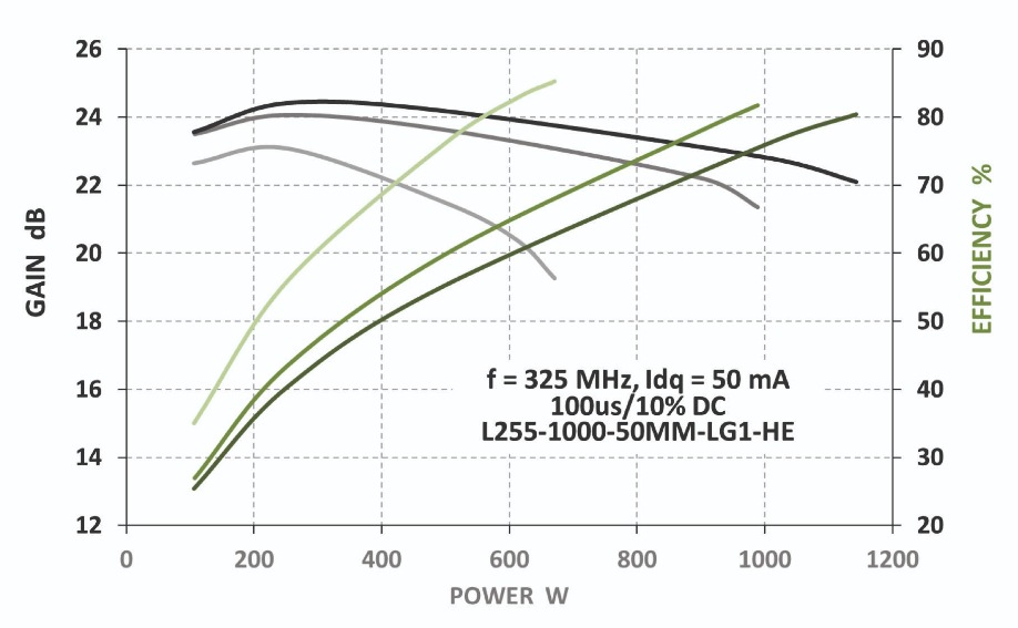
Figure 2. Measured RF power gain and drain efficiency versus output power for a 50 mm die with a signal of 100 µs pulse width and 10 percent duty cycle at 325 MHz. The device is characterized at 100 V, 125 V and 145 V DC bias demonstrating a 3 dB power dynamic range. By reducing operating bias to 50 V a 6 dB dynamic range is achieved.
Our R&D activities have extended to considering the bandwidth associated with the higher power densities and higher load impedances at 100 V and 150 V. Power-over-bandwidth is a ‘hot button’ in several applications, with requirements that may be strictly application-specific and not discussed in the public domain. What we can say, nonetheless, is that broadband high-power applications are destined to reap huge benefits from our 100 – 150 V amplifier technology.
System-level benefits
As mentioned earlier in this article, the higher voltage GaN transistors can achieve power densities of more than 20 W/mm, thus allowing for reduced circuit complexity for the same relative power level. As an example, two 1 kW transistors running at 50 V could be replaced by a single 2 kW transistor operating at 100 V. This eliminates one transistor and the combining structure required for the lower voltage solution.
Another advantage of a higher voltage is evident in a simple load-line analysis. While a 50 V device will provide a 25 W output power with just a 50 Ω load, a 100 V device will provide four times this power.
For broadband applications, higher voltage GaN HEMTs can also be an advantage, considering that the device impedances increase with higher voltage operation and the capacitance-per-Watt are reduced.
Lower voltage solutions require larger impedance transformations to achieve bandwidth, while a higher voltage solution can eliminate these transformers or reduce transformation ratios and their complexity. When utilizing 100 V GaN, the matching structure size can be reduced by a factor of two or more by removing transformers over a 50 V GaN solution for the same RF output power.
There is no doubt that much is to be gained from increasing the operating voltage of the GaN HEMT. There are benefits for the device itself, including an increase in output power, plus plenty of advantages at the circuit and system level. Our company is in talks with several VED’s users to commercialize our high-voltage GaN/SiC green technology.


Exposure to a nitrogen plasma enhances field-effect mobility in GaN vertical-channel MOSFETs
ENGINEERS at Nagoya University, Japan, are claiming to have broken new ground by unveiling a simple process to improve the channel of a GaN trench MOSFET. Their effort will help to advance the capability of the GaN trench MOSFET, which has the upper hand over other classes of GaN transistor in realising a lower specific on-resistance, thanks to a narrower cell pitch that results from the use of a vertical channel.
The team from Nagoya University have increased channel mobility in the GaN trench MOSFET with a two-step process that involves an in-situ nitrogen plasma treatment in an atomic layer deposition (ALD) chamber, followed by deposition of a gate insulator GaN channel. “Any special equipment or extensive process is not necessary,” points out team spokesman Takashi Ishida.
A high channel mobility results from the compensation of nitrogen vacancies within a device – this is said to be a ground-breaking accomplishment. The reduction in vacancies combats Coulomb scattering, which is known to inhibit channel mobility.
Merits of the nitrogen plasma process are underscored by electrical measurements on a portfolio vertical trench MOSFETs, which have been formed with different treatments to the sidewalls.
Fabrication of the MOSFETs began by loading an n-type GaN substrate into an MOCVD chamber and depositing a 2 µm-thick p-type body layer, followed by a 100 nm-thick p-type contact. To aid analysis of channel properties, the team omitted the drift layer, as this allowed them to exclude drift resistance.
The next steps in the fabrication process involved activation of p-type layers by high-temperature annealing, the addition of a 500 nm-thick SiO2 mask and selective etching of the p-type contact layer. Deposition of a 200 nm-thick n-type source layer over the whole surface followed, prior to selective etching with tetramethylammonium hydroxide (TMAH).
Ishida and co-workers used sputtering, rather than ion implantation, to create dopants in the n-type source layer. They took this approach because sputtering does not require high-temperature annealing at 1000 °C, a step that could introduce defects in the p-type body layer where the channel is formed. Note that defects in this region could also result from ion implantation.
To form the trench structure, the team employed multi-step bias etching. After this, they subjected the structure to a 30 minute nitrogen plasma treatment in an ALD chamber, using an output power of 300 W and argon and nitrogen flows of 130 sccm and 20 sccm, respectively.
Final steps for device fabrication involved ALD and annealing of a 35 nm-thick layer of Al0.78Si0.22O that formed the gate oxide, and then the addition of a poly-silicon gate electrode and metal stacks to create source, drain and p-type body contacts.
Secondary ion mass spectrometry revealed that silicon did not diffuse into the p-type body layer. Magnesium diffusion into the n-type source did occur, but levels were more than three orders of magnitude lower than that for the silicon dopant, so had negligible impact. Electrical measurements determined that plasma treatment led to an increase in field-effect mobility from 30 cm2 V-1 s-1 to 47 cm2 V-1 s-1, leading the team to conclude that plasma treatment is effective at improving the channel properties of vertical trench GaN MOSFETs.
The engineers are now making a vertical trench GaN MOSFET with a drift layer. According to Ishida, as it is important to also realise a desired breakdown voltage, in parallel the team are developing an edge-termination structure.

Engineers at Nagoya University, Japan, have increased the mobility of the channel in vertical GaN MOSFETs by turning to an in-situ nitrogen plasma treatment in an atomic layer deposition chamber.
T. Ishida et al. Appl. Phys. Express 13 124003 (2020)

Quashing interface states in SiC MOSFETs
To trim channel resistance, the production of SiC MOSFETs should include etching with hydrogen gas, deposition of silicon dioxide by CVD, and a nitridation process
THE SiC MOSFET, widely viewed as the best commercial device for fast switching at high voltages, is compromised by a high channel resistance that stems from a high density of interface states.
But this weakness can be overcome, thanks to a novel three-step process that has recently been developed by a team from Kyoto University, Japan.
Using techniques such as secondary ion mass spectrometry and deep-level transient spectroscopy, the researchers found that defects are generated near the SiC-SiO2 interface during thermal oxidation, the standard process used to make the gate oxide of a SiC MOSFET. To quash these defects, they have developed a process that involves etching SiC with hydrogen gas before depositing a SiO2 film by plasma-enhanced CVD and using nitridation with N2 gas to passivate defects at the SiC-SiO2 interface.
Spokesman for the team, Tsunenobu Kimoto, points out that he and his colleagues are by no means the first to create the SiO2 film by deposition, rather than thermal oxidation. Up until now, though, deposition processes proved unsatisfactory, due to defects generated during sacrificial oxidation that are located up to 5 nm below the surface. “We solved this problem by appropriate hydrogen etching before silicon dioxide deposition,” explains Kimoto.
Another recent approach for forming a high-quality SiC MOS interface involves the use of supercritical CO2 (see Compound Semiconductor, Nov & Dec 2020, p. 66). However, according to Kimoto, this alternative fails to deliver a significant reduction in defect density, while their approach reduces this by a factor of 30 to 50.
The process developed by engineers at Kyoto University will aid designers of SiC MOSFETs, because it increases the range of dimensions that can be used for this class of transistor. By reducing resistance through a lowering of the interface states, it is possible to employ shorter channels while avoiding short-channel effects, such as a decreasing threshold voltage and a degradation in sub-threshold slope that leads to the need for larger switching voltages. When SiC MOSFETs are made with conventional processes, short-channel effects start encroaching at channel lengths below 1 µm.
To investigate the impact of interface states on different processes used to add and treat the SiO2 film, Kimoto and co-workers fabricated a portfolio MOS capacitors on n-type 4H-SiC (0001) epilayers. As part of this study, they investigated whether the benefits of the nitridation process were simply due to the high temperature employed – it takes place at 1400 °C – or resulted from the use of N2 gas. To test the latter, the team compared results with those associated with a similar process involving argon. The engineers also fabricated MOS capacitors by dry oxidation to aid comparison.
Values for the density of interface state for MOS capacitors produced with various processes are shown in the figure (see above). The lowest dispersion came from H2 gas etching, followed by SiO2 deposition and nitridation (“H2-CVD-N2”).
Kimoto and colleagues are now using their process to produce and evaluate SiC MOSFETs. Initial results are encouraging, with channel mobility increasing from 38 cm2 V-1 s-1 to 85 cm2 V-1 s-1. Dielectric breakdown characteristics of the gate oxide and the threshold-voltage stability are said to be “very good”.
The team intends to make additional refinements to its process. “[We] would like to show a high channel mobility over 100 cm2 V-1 s-1in n-channel 4H-SiC(0001) MOSFETs,” says Kimoto.

Interface defects in MOSFETs fall by the combination of H2 gas etching, SiO2 deposition and nitridation (“H2-CVD-N2”). The un-annealed sample, labelled “As-Ox”, suffers from a large frequency dispersion. Reduced dispersion came from the processes: “CVD-N2”, which involved SiO2 deposition and a N2 gas anneal; “Ox-N2”, a combination of dry oxidation and a N2 gas anneal; and “OX-NO”, which involves dry oxidation and NO annealing at 1250 °C.
K. Tachiki et al. Appl. Phys. Express 13 121002 (2020)
Intentional degradation induces the introduction of interstitial indium in the quantum wells
RESEARCHERS IN CHINA are claiming to have shed new light on changes that occur within a green-emitting GaN LED as it degrades.
The experimental and theoretical study conducted by the team from Shaanxi University of Science and Technology and Taiyuan University of Technology concluded that degradation resulted in red-shifted LEDs with a reduced luminous efficiency. These changes were attributed to three factors: decreased bandgap, caused by relaxation of the InGaN quantum well; increased defect density, due to the introduction of interstitial atoms; and increased InGaN quantum well thickness.
LEDs employed in the investigation were fabricated in-house. The devices, grown in an Aixtron MOCVD reactor on 2-inch c-plane sapphire substrates, featured nine 15.6 nm-thick In0.28Ga0.72N quantum wells separated by 3.1 nm-thick GaN quantum barriers. LEDs subjected to degradation were heated to 460K for 3 hours.
High-resolution X-ray diffraction curves for pristine and degraded LEDs revealed satellite peaks up to the fifth order, indicating “acceptable” crystalline quality for the wells and the interface quality. Curve fitting suggested a thickness period of 18.5 nm, a value in good agreement with device design. A slight widening of the first diffraction peak for the annealed LED indicates that the high-temperature, degradation-inducing step led to a reduction in the quality of the crystalline material and the interface.
All these conjectures are confirmed with scanning tunnelling electron microscopy high-angle annular dark field images that identify atomic columns of InGa and gallium. These images reveal that after annealing, InGa and gallium atomic columns become indistinct, reflecting a deterioration in the quality of the crystal and the interface.
An additional insight provided by these images is the change in the thickness of the layers within the active region. Degradation induced an increase in the thickness of 11 atomic layers in the InGaN quantum well from 285 nm to 308 nm in the [0002] direction, and an increase from 2.85 nm to 308 nm in the [1010] direction. For the GaN barrier, a far smaller change took place, with the thickness of 28 atomic layers in the barrier increasing from 8.17 nm to 8.19 nm in both the [0002] and [1010] directions.
Another finding from these dark-field images is that annealing created additional atomic columns. Based on this observation, and the others obtained with this imaging technique, the team concluded that the introduction of interstitial atoms is behind the increase in thickness of the InGaN wells.
According to the researchers, elevating the temperature of the LED to 460K resulted in intense atomic lattice vibrations that caused the indium atoms to migrate from their normal lattice position to interstitial sites. Electroluminescence measurements determined that annealing at 460K led to a 1.6 nm red-shift in peak emission from 519.9 nm to 521.5 nm, and a fall in integrated intensity by 32.8 percent. The annealed device produces stronger luminescence at 650 nm, a peak associated with impurities and defects. When LEDs have a higher density of defects, luminescence is known to fall, due to increases in both defect-related Shockley-Read-Hall recombination and Auger recombination.
To gain greater insight into how the emission characteristics of the quantum well are influenced by gallium interstitial atoms, and gallium and nitrogen vacancies, the team turned to density functional theory based on first principles calculations. This theoretical study revealed that the red-shift of the LED and its decline in efficiency resulted from: a decreased bandgap, due to relaxation in the InGaN well; and a hike in defect density, due to the introduction of interstitial indium atoms within the active region.

Degradation of green LEDs produces a small shift in wavelength and a reduction in efficiency.
Q. Liu et al. Appl. Phys. Lett 117 212103 (2020)
Beneq TransformTM © All rights reserved.
DRIVEN by fast-growing demand in electric vehicles, consumer electronics and renewable electricity modern power devices are evolving rapidly in terms of materials as well as design and process technologies. For example, Wide Bandgap SiC and GaN devices have the fundame ntal advantage of low on-resistance x
high breakdown voltage. Increasingly advanced deposition technologies are required across the board. The most critical are the dielectrics to be grown or deposited at the surface of the semiconductor, either as part of the active MOS or MIS structure or as a surface passivation layer.ALD holds unique advantages over other deposition methods such as PECVD
Proprietary Beneq in-situ pre-clean and passivation is especially developed for metal and semiconductor surfaces – Silicon and compound semiconductor. In other words, ALD also differentiates by its capability to grow thin dielectrics of thermal quality at much lower temperature than thermal processes such as thermal oxidation. ALD enables low thermal budget process integration. Not only SiC and GaN devices but also mainstream MOSFET’s and IGBT benefit from the above merits enabled by advanced integrated ALD technology. Thanks to rapid advances in ALD equipment technology, throughput can now be scaled by using batch process i.e. 25 wafer batch as much as needed. Thermal batch ALD enables production-worthy throughputs (double digit) for thickness in the range of 10 to 100 nm.

Beneq TransformTM platform overview © All rights reserved.
Beneq TransformTM cluster tool is a fully automated, in-vacuum cassette-to-cassette ALD manufacturing solution
“The Beneq TransformTM mainframe is built on an industry-standard handling system, equipped with a four-sided – Beneq TransformTM Lite – or six-sided transfer module including one or two cassette load locks for production worthy reliable cassette-to-cassette full single wafer automation. The configuration is highly flexible and scalable and can be adapted to various R&D and manufacturing requirements for wafer sizes from 3’’ up to 8’’,” says Dr. Patrick Rabinzohn, Business Executive, Semiconductor ALD Business Line.
The Beneq TransformTM can be configured with or retrofitted with Beneq single wafer thermal and/or plasma as well as batch ALD process modules. Its proprietary preheating module nearly eliminates heating related waiting time, boosting productivity to a whole new level. In addition, the mainframe accommodates an optical aligner, and can be equipped with optional integrated Brooks TopCoolerTM cool-down unit, and internal wafer buffer. The Beneq TransformTM is fully compliant with ultra-clean requirements, SECS/GEM communication and SEMI S2 and S8 standards certified.
Designed with versatility at heart
Beneq TransformTM can be used to deposit a wide range of oxides, including Al2O3, HfO2, Ta2O5, TiO2 and SiO2 using thermal single wafer or batch ALD, and nitrides such as AlN, Si3N4 using plasma enhanced ALD. In addition to oxides, thermal batch processing up to 25 wafers for nitrides such as AIN and TiN requiring high processing temperatures is supported. Beneq TransformTM is the leading choice for all More-than-Moore applications. It is configured to have the smallest footprint and lowest cost-of-ownership for any of the very diverse process capabilities x capacity requirements of the MtM market segments shown below.

Beneq ALD solutions for More-than-Moore markets.
Additionally, Beneq single wafer process module comes with high degree of built-in processing versatility, which is particularly beneficial in processing sensitive materials such as SiC, GaN, GaAs, and InP. Firstly, the plasma ALD module can be used for efficient in-situ surface pre-clean/nitridation, which is crucial for eliminating surface states associated with non-stoichiometric oxides. A further benefit is the capability of sequencing of plasma/thermal nitrides and thermal/plasma Oxide processes in the same chamber either as bi-layer or as laminates/mixtures, without the need to transfer the wafer from a nitride chamber to an oxide chamber. A further processing option is the possibility to switch the plasma enhanced ALD module to thermal ALD processing only, by a simple change kit.
In a nutshell from single wafer and batch process modules to single wafer sequential and parallel processing versatility is at the heart of BENEQ Transform™.

Beneq is the home of ALD, offering a wide portfolio of equipment products and development services. Today Beneq leads the market with innovative solutions for advanced R&D (TFS 200, R2), flexible high-volume manufacturing (BENEQ TransformTM), ultra-fast high precision spatial ALD coatings (C2R), roll-to-roll thin film coating of continuous webs (WCS 600), and specialized batch production for thicker film stacks (P400, P800). Headquartered in Espoo, Finland Beneq is dedicated to making ALD technology accessible for researchers and enabling technology mega trends through engineered ALD materials solutions.
For Inquiries
Lie Luo, Marketing Manager