DO YOU EVER WONDER why some records last for longer than others? I expect it’s linked to the setting of new benchmarks that are not incremental, but substantial, and could take decades to eclipse. Think, for example, of Bob Beamon’s legendary leap in the Mexico Olympics of 1968 that held the record for 23 years – or when Usain Bolt ran the 100 metres at the 2009 World Athletics Championships in a time of just 9.58 seconds, smashing his previous world record. But there are other reasons why a record may stand for so long, such as dwindling interest in extending what is possible, and a need for a radical change to break new ground.
There is an element of all these factors at play in the efficiency record for the solar cell. When cash flowed freely in the fledging concentrating photovoltaic industry, records tumbled, as companies strived to gain a competitive edge by developing the best solar cells. It’s not surprising that records are lasting longer since funding has dried up and some companies have disappeared.
Also applying the brakes to any claim of a record-breaking efficiency is the need for radical designs. Once triple-junction variants neared their limit, additional junctions were needed to break records.
Back in late 2013 the French firm Soitec adopted this approach, setting a new benchmark with a four-junction device, created by bonding together a pair of dual-junction devices. This raised the record from 44.4 percent to 44.7 percent. And a year later, a refined variant realised 46 percent. Although that extra 1.3 percent might not sound much, it is a substantial gain.
This record stood for many years. Only recently has it been broken by a team from the NREL. They have developed a six-junction cell with an efficiency of 47.1 percent – and an even higher figure could follow, with an expectation of exceeding 50 percent if the resistance can be trimmed to values found in triple-junction cells.
NREL’s work, detailed in the feature Six-junction super cells, built on the inverted metamorphic design pioneered in this lab. However, to make the latest device required a far more extreme grading of lattice constants, and the development of new tunnel junctions.
Ideally, this work will lead to a greater use of terrestrial cells based on III-Vs. Success will not be easy, due to high costs, but the team from NREL are hoping to address that issue by developing new growth techniques. I wish them well in this endeavour.

CREE has announced that Zhengzhou Yutong Group, a large-scale industrial Chinese manufacturer of commercial vehicles that specialises in electric buses, is using Cree 1200 V SiC devices in a Starpower power module for its new high-efficiency powertrain system for electric buses. The use of SiC-based power solutions enable faster, smaller, lighter and more powerful electronic systems for commercial electric vehicles.
The parties are working together to accelerate the commercial adoption of SiC-based inverters in electric bus applications. Upon rollout, Yutong Group will deliver their first electric bus in China to use SiC in its powertrain, representing a significant advancement in providing an even more efficient e-bus to the market.
“Cree and StarPower’s collective effort in driving the innovation of SiC technology perfectly fits with Yutong’s high-end roadmap of powertrain products.” said Wei Wei, General Manager, Electronic Devices Business Unit Yutong Group. “Yutong is committed to helping travelers experience the comfort and beauty of the world through sustainable bus travel, and this collaboration ensures we are able to provide an even more efficient electric bus through the benefits of SiC.”
Coupled with StarPower’s power module technology, the use of Cree’s SiC-based MOSFET in the powertrain will help extend driving range while lowering weight and conserving space.
“StarPower entered the new energy vehicle market in 2008 and, in that time, we have won the recognition from worldwide new energy vehicle customers as a leader in the space. It’s our great honor to become the power module supplier of the Yutong powertrain system,” said Shen Hua, CEO of StarPower. “We are committed to bringing customers more state-of-the-art products and will continue strengthening our competitiveness.”
Cree is currently expanding manufacturing capacity to support the expected growth of the electric vehicle marketplace. In 2022 the company plans to open the world’s largest SiC fabrication facility in New York while at the same time expanding SiC crystal growth capacity at its operations in North Carolina. The company offers its SiC and GaN power and RF solutions through its Wolfspeed business unit.
“Cree’s technology is at the heart of the dramatic change underway in electric vehicles for the commercial and consumer markets, and we are committed to supporting the industry as it transitions to more efficient, higher performing SiC solutions,” said Gregg Lowe, CEO of Cree. “The work with StarPower and Yutong Group is a great example of how strong partnerships can deliver innovative solutions to the marketplace. As the world leader in SiC, Cree is continuing to expand capacity to meet market demands with our industry-leading power MOSFETs to help achieve a new, more efficient future.”
As a power module supplier in the China market, StarPower provides a complete range of industry-leading power modules to customers. In 2017, StarPower’s automotive module production headquarters was founded in Shanghai China, which enables the company to provide customers even better capacity and quality guarantees.
SINGAPORE-BASED robotics manufacturer Otsaw Digital has launched the world’s first UV-C LED Disinfection Autonomous Robot. Otsaw has filed the relevant patents for this new innovation which it calls O-RX .
From conceptualisation, design, materials procurement, prototype testing to certification, the development of the O-RX was successfully completed in eight weeks. The O-RX has undergone the relevant safety and testing under various conditions and has been certified by internationally-accredited TUV SUD.
Eliminating the use of mercury lamps that emits harmful UV-A and UV-B radiations, the O-RX uses UV-C LED technology that emits only UV-C light, which is extremely effective when it comes to killing microbes, including harmful bacteria and coronaviruses such as COVID-19. Hence, the UV-C LED technology is
Integrated with the UV-C LED technology, the O-RX is said to have a disinfection rate of more than 99.999 percent with a range of 2.5 metres and the UV-C LED technology is also more energy efficient than conventional mercury lamps by 70 percent.
Capable to be deployed for five hours on one full charge, the O-RX is also equipped with a 360-degree camera and LIDAR sensors with self-driving, collision avoidance and artificial intelligence technologies. The O-RX can be controlled and managed remotely via a fleet management control platform that is developed by Otsaw.
To help remove heat generated by the LED, the robot uses a thermal management solution developed by researchers at the Agency for Science, Technology and Research’s (A*STAR) Singapore Institute of Manufacturing Technology (SIMTech).
Otsaw will be collaborating with YTL Starhill Global REIT Management, the manager of Starhill Global REIT, and
will be running a trial of the O-RX at Wisma Atria commencing from 15 July 2020. Otsaw’s founder and CEO, Ling Ting Ming, commented: “Disinfection is a key part of protecting the health and safety of communities and more than ever, we need to accelerate the rate of automating disinfection as COVID-19 outbreak increased the demand and frequencies of disinfection but at the same time, manpower resources have been curtailed.
“O-RX combines innovative LED technology and robotics to allow the disinfecting process to be fully autonomous, mobile and much safer, thereby achieving a higher disinfection efficiency as compared to conventional methods and reduce the dependence of human resources.”

RESEARCHERS at the University at Buffalo have developed a Ga2O3-based transistor that can handle more than 8,000 V.
They think the transistor could lead to smaller and more efficient electronic power systems in electric cars, trains and airplanes. In turn, this could help improve how far these vehicles can travel. They published the results in the June edition of IEEE Electron Device Letters.
“To really push these technologies into the future, we need next-generation electronic components that can handle greater power loads without increasing the size of power electronics systems,” says the study’s lead author, Uttam Singisetti, who adds that the transistor could also benefit microgrid technologies and solid-state transformers.
Singisetti, associate professor of electrical engineering at the UB School of Engineering and Applied Sciences, and students in his lab have been studying the potential of Ga2O3, including previous work exploring transistors made from the material.
Ga2O3 has a bandgap of about 4.8 eV, which places it among an elite group of materials considered to have an ultrawide bandgap. SiC is 3.4 eV and GaN around 3.3 eV. Bandgap measures how much energy is required to jolt an electron into a conducting state. Systems made with wide-bandgap materials can be thinner, lighter and handle more power than systems made of materials with lower bandgaps.
A key innovation in the new transistor revolves around passivation to reduce the chemical reactivity of its surface. To accomplish this, Singisetti added a layer of SU-8, an epoxy-based polymer commonly used in microelectronics.
Tests conducted just weeks before the Covid -19 pandemic temporarily shuttered Singisetti’s lab in March show the transistor can handle 8,032 V before breaking down, which is more than similarly designed transistors made of SiC or GaN that are under development.
“The higher the breakdown voltage, the more power a device can handle,” says Singisetti. “The passivation layer is a simple, efficient and cost-effective way to boost the performance of Ga2O3 transistors.”
Simulations suggest the transistor has a field strength of more than 10 million volts (or 10 megavolts) per centimetre. Field strength measures the intensity of an electromagnetic wave in a given spot, and it eventually determines the size and weight of power electronics systems.
“These simulated field strengths are impressive. However, they need to be verified by direct experimental measurements,” Singisetti says. The research was supported by the US Air Force Office of Scientific Research and by the US National Science Foundation.
TAIWAN-BASED LED manufacturers Epistar and Lextar announced their plan to jointly establish a holding company through share conversion. TrendForce’s LEDinside research division offers the following comments regarding the two companies’ partnership:
With the rise of micro LED and mini LED commercial opportunities, leading manufacturers such as Apple and Samsung are placing high hopes in the future of these two emerging display technologies and forecasting a high demand for micro/mini LED suppliers’ production capacities. However, as Taiwanese LED manufacturers have suffered continuous financial losses over the past few years, most of them can no longer afford to expand their production capacity on a large scale to meet demands from end-product brands. Furthermore, the recent surge in CAPEX by Chinese LED chip manufacturers and LED packaging companies, as well as their partnership with domestic panel manufacturers, has alarmed Taiwanese LED companies to the hypercompetitive state of the LED industry.
By forming a holding company, Epistar and Lextar are now able to jointly bear the enormous burden of investing in new equipment, in turn lowering their operational risk and helping them gain a foothold in the market for new types of displays. TrendForce estimates that Epistar and Lextar will collectively account for 12.43 percent of the global LED chip production capacity after the formation of the holding company.
Epistar’s production capacity is primarily focused on LED epitaxy and LED chip fabrication, whereas Lextar specialises in LED packaging and modules. The partnership between the two companies will result in a total vertical integration throughout the entire LED industrial supply chain. Given that both companies have been actively investing in mini LED backlight R&D, the collaboration between Epistar and Lextar will serve to reduce their competition with each other over client orders as mini LED backlight demand from panel manufacturers and branded end-product OEMs skyrockets.

ASIA-AFRICA-EUROPE-1 Consortium (AAE-1), one of the largest consortium cable systems, has recently completed a significant upgrade with Infinera to boost capacity on its subsea network connecting East Asia to Europe via Egypt.
AAE-1 has proved to be vital infrastructure in the Eurasia corridor, and even more so recently, providing connectivity, diversity, and resilience between European, Asian, and Middle Eastern markets. Based on Infinera’s fourth-generation Infinite Capacity Engine (ICE4) technology and Instant Bandwidth capability, the Infinera solution enabled AAE-1 to double the capacity on its intercontinental network while reducing total cost of ownership and increasing service agility and network reliability.
AAE-1’s cable system spans 25,000km of subsea and terrestrial network. Unlike any other cable system in the world, AAE-1 terminates at two points of presence in Singapore and is claimed to be the only next-generation cable that continues further into Asia through diverse terrestrial routes across Thailand, providing connectivity to Vietnam, Cambodia, and Hong Kong.
This routing enables AAE-1 to deliver a low-latency routes between Hong Kong, India, the Middle East, and Europe.
“AAE-1 is an important subsea cable asset for carriers globally, with bandwidth needs growing rapidly, particularly during this very difficult and deeply sad global crisis. After a rigorous evaluation, we selected Infinera for its superior reach, optical transmission performance, and reliability,” explained Loucas Balis, chairman, AAE-1 Management Committee.
“When selecting a solution for AAE-1, it was critical to select a vendor with a seamless scalable solution for the entire network, with great economics,” Giuseppe Sini, vice chairman, AAE-1 Management Committee added. “Infinera gave AAE-1 the ability to activate capacity quickly and really differentiate our services. Infinera has been an excellent choice.”
“We are pleased to support AAE-1’s network upgrade, delivering the benefits of Infinera’s photonic integrated circuit-based ICE4 solution, featuring industry-leading spectral efficiency, Nyquist subcarriers, SD-FEC gain sharing, and Smart Optimise.
The deployed solution also delivered extended C-band open line system terrestrial crossings that are expandable in-service to L-band,” said Nick Walden, SVP, Worldwide Sales at Infinera.
“By deploying Infinera’s subsea solution, AAE-1 is set up for success now and into the future, with pioneering technology to tackle next-generation services, including Instant Bandwidth functionality that enables unlocking additional network capacity through remote activation.”

CEA-LETI has announced its researchers have broken the throughput world record of 5.1 Gbit/s in visible light communications (VLC) using a single blue GaN microLED. Their data transmission rate of 7.7 Gbit/s achieved with a 10 µm microLED marks another step toward commercialisation and widespread use of LiFi communication.
VLC, commonly called LiFi (short for ‘light fidelity’), is an emerging wireless communication system that offers an alternative or a complementary technology to radio frequency (RF) systems such as WiFi and 5G. It is considered to be a promising technology for security-related applications because light propagation can be confined to a room with no information leakage, as opposed to WiFi communication, which penetrates walls. LiFi also holds promise for ultra-highspeed data transmission in environments where RF emissions are controlled, like hospitals, schools, and airplanes.
Single microLED communications offer an ultra-high data-transmission rate for a variety of opportunities for new applications. These include industrial wireless high-speed links in demanding environments such as assembly lines and data centres, and contact-less connectors, or chip-to-chip communication. But their weak optical power limits their applications to short-range communications.
In contrast, matrices of thousands of microLEDs contain higher optical powers than open mid- and long-range applications. However, preserving the bandwidth of each microLED within a matrix requires that each signal has to be brought as close as possible to the micro-optical source.
Mass-market applications
CEA-Leti’s expertise in the microLED epitaxial process produces microLEDs as small as 10 microns, which is among the smallest in the world. The smaller the emissive area of the LED, the higher the communication bandwidth – 1.8 GHz in the institute’s single-blue microLED project. The team also produced an advanced multi-carrier modulation combined with digital signal processing. This high-spectrum-efficiency waveform was transmitted by the single LED and was received on a high-speed photodetector and demodulated using a direct sampling oscilloscope.
“This technology has exciting potential for mass-market applications,” said Benoit Miscopein, CEA-Leti research scientist. “Multi-LED systems could replace WiFi, but wide-scale adoption will require a standardisation process to ensure the systems’ interoperability between different manufacturers. The Light Communications Alliance was created in 2019 to encourage the industry to implement this standardisation.”
In addition to a stand-alone WiFi-like standard, the possibility to include this new technology as a component carrier in the downlink of 5G-NR, a radio-access technology for 5G mobile considerations, is also under investigation to bring a large additional license-free bandwidth.
“This may be feasible because CEA-Leti’s LiFi physical layer relies on the same concepts as WiFi and 5G technologies,” said Miscopein. “Matrices of thousands of microLEDs could also open the way to mid- to long-range applications, such as indoor wireless multiple access.”
Preserving the bandwidth of each microLED within a matrix requires that each signal is generated as close as possible to the micro-optical source.
“To meet this challenge, we expect to hybridise the microLED matrix onto another matrix of CMOS drivers: one simple CMOS driver will pilot one microLED,” Miscopein said. “This will also enable the additional feature of piloting each microLED pixel independently, and that allows new types of digital-to-optical waveforms that could eliminate the need for digital-to-analog converters commonly used in the conventional ‘analogue’ implementations of LiFi.”
While the Light Communications Alliance will promote interoperability between different manufacturers’ LiFi systems, CEA-Leti will continue its research in two areas: a better understanding of the electrical behaviour of single LEDs in high frequency regimes and the link between bandwidth and electromigration patterns, and; techniques to improve the range and/or increase the data rate using multi-LED emissive devices.
This requires adapting the waveform generation as well as a CMOS interposer to drive the matrix on a pixel basis.

CONTINENTAL Vitesco Technologies’ powertrain business and Rohm Semiconductor have signed a SiC development partnership, beginning in June 2020. Vitesco Technologies will use SiC components to further increase the efficiency of its power electronics for electric vehicles (EV).
Through their higher efficiency SiC semiconductors make better use of the electric energy stored in a vehicle battery. Thus, an EV has a longer range, or the battery cost can be reduced without impacting the range.
“Energy efficiency is of paramount importance in an electric vehicle. As the traction battery is the only source of energy in the vehicle, any losses caused by power conversion need to be minimised. We are therefore developing a SiC option within our modular power electronics system,” says Thomas Stierle, executive VP of the Electrification Technology business unit at Vitesco Technologies.
“To get the maximum efficiency out of the power electronics and the e-motor we will use SiC power devices from our preferred partner. Rohm has convinced us of its products.”
“We are looking forward to the future cooperation with Vitesco Technologies”, says Kazuhide Ino, corporate officer, director of power device business unit at Rohm. “We are the leading company in SiC power semiconductors and have achieved a significant technological lead in this field along with the provision of power solutions combined with gate driver ICs. Together with Vitesco Technologies we want to further improve the energy efficiency of the electronic system in EVs to use the full potential of the SiC technology for a sustainable mobility.”
Vitesco Technologies is already developing and testing SiC technology in an 800 V inverter concept to confirm the efficiency potential of the technology.
The approach of this program is to look at the complete system of inverter and motor to identify the best combination of device technology and switching strategy.
In this context SiC semiconductors – e.g. for example, SiC MOSFETs for 800 V battery systems – offer more efficient switching in the inverter (higher frequency, steeper switching slopes) and cause fewer harmonic losses in the electric motor. Also, SiC technology is a key enabler for super-fast charging technology that uses 800 V. In the course of the cooperation Rohm and Vitesco Technologies will work on creating the optimum combination of Rohm’s SiC technology for high volume manufacturing and best fit of inverter design for highest efficiency.
“The SiC option is a very promising future part of our modular power electronics system comprising of software, power output stage, and switching strategy”, says Gerd Rösel, Head of Innovation in the Electrification Technology business unit at Vitesco Technologies.
“We will work with Rohm on a 800-volt SiC inverter solution as well as on a 400-volt SiC inverter solution.”
Vitesco Technology plans the start of production of the first SiC inverter as of 2025, when the demand for SiC solutions is expected to rise significantly. “In other words, our partnership and development are perfectly on time”, says Rösel.
The preferred partnership will also be benefiting from short distances: Vitesco Technologies and Rohm both have sites at Nuremberg (Rohm Semiconductor Group: SiCrystal GmbH), which in turn is not far from Vitesco Technologies’ headquarters at Regensburg.

With the Class D audio amplifier market poised for massive growth, GaN Systems has set its sights on snaring a big chunk of the sector, reports Rebecca Pool.
WHEN IT COMES to the wonderful world of audio, not all solid-state amplifiers are created equal. For decades, the analogue-based linear amplification Class A audio system has reigned supreme, with audiophiles tolerating its very low efficiency.
Not anymore. Today, a growing number of power semiconductor suppliers are delivering a new breed of GaN-based Class D audio amplifier that promises far higher power efficiencies than your archetypical Class A amplifier.
For example, Infineon Technologies has developed its ‘MERUS’ class D audio amplifier ICs that are said to maximize power efficiency and dynamic range while providing stunning audio performance in small product form factors. And GaN Systems has recently released a Class D amplifier evaluation kit that also promises to deliver unprecedented efficiency and sound quality.
“When some of my very discerning customers from Japan first listened to our GaN amplifier, they told me that it was like arrows of sounds coming from the speaker,” says Rick Reigel, Vice President of Sales at GaN Systems. “On closing their eyes they said they could feel the music and it felt as if it were live, rather than an artificially reproduced sound – this is the kind of reaction that we get.”
Gathering momentum
Operating as electronic switches rather than linear gain devices, Class D amplifiers were initially developed in the 1950s. However, these systems didn’t truly reach the market until the 1990s, with the advent of adequate-performing silicon MOSFETs.
Historically, these systems have been relegated to lower-quality audio systems as the use of silicon can lead to audio distortion arising from imperfect switching and high on-state resistance. However, Reigel is confident that the new wave of GaN MOSFET-based amplifier systems will change this, offering sound quality as well as higher efficiencies.
“GaN is going to continue the curve of improvement and can deliver a smaller, lighter, more efficient amplifier,” he says. “The GaN MOSFET ensures much cleaner switching, enabling better linearity in the amplifier as well as less intermodulation distortion, which means [suppliers] can continue to shrink amplifier size without sacrificing sound quality, which is a trend we’re seeing across the industry.”
“We can get a high-fidelity sound using GaN in this Class D topology, as well as this great blend of size, weight, efficiency and cost,” he adds. “This is the real value proposition of GaN in this application, and you just can’t achieve it in any other way.”
GaN Systems’ recent evaluation kit includes a 2 channel, 200 W-per-channel class D audio amplifier and companion 400 W continuous power audio-grade switched-mode power supply (SMPS) without heatsinks. A single GaN FET design is used for front-end power factor correction with a dual GaN FET half-bridge used for the back-end SMPS.
Crucially, the set-up allows for a low-cost three FET design that doesn’t demand a massive external heat-sink for full-power operation. And GaN Systems has also developed a low inductance GaN transistor package.
“In the pre-amplifier part of the design, we have a lot of silicon and this links to the audio source, say, a CD player or music files,” highlights Reigel. “If you want to drive a stereo application with the full bridge, then there’s actually eight GaN transistors in the output stage, just prior to the speaker.”
Right now, the company is seeing a growing demand for smart and battery powered speakers, multi-channel automotive and high-end home-audio systems, and is also targeting traditional home theatre and professional audio markets, including stadiums. And according to Reigel, feedback from reviewers in the audio industry, so far, is good.
“We’ve taken our systems to the [Consumer Electronics Show] CES and carried out a side-by-side test with a silicon Class D amplifier,” he says. “We got a great response – you literally hear the difference right away, and we believe we can provide a premium sound with a consumer price.”
Reigel reckons for the transistors alone, this audio market is worth somewhere between $3.5 bilion and $4 billion, and has a compound annual growth of up to 10 percent. “GaN has an opportunity to grow very fast here as it’s substituting for silicon in a market that already exists,” he says. “Right now we’re only encroaching on silicon here but I believe that eventually GaN will take the majority of the market, which is very nice for GaN transistor suppliers.”
What’s more, the Vice-President of Sales doesn’t believe that competing technology, SiC, is a threat. As he puts it: “Silicon carbide is great for certain applications but still has a reverse recovery problem, so doesn’t quite cut it in this application.”
So where next for GaN Systems and Class D amplifiers? Reigel is confident that GaN Systems is set to be a frontrunner in the Class D amplifier market, which, he is sure, will switch entirely from silicon to GaN in around a decade.
“In five years I think GaN will have around 50 percent of this market and will hold close to 100 percent in ten years,” he says.
“GaN is still in its infancy and there are still years of improvement ahead of us – over the next five years to a decade, we will see more improvements to the GaN transistor and these will directly benefit the audio amplifier,” he adds. “This is a huge market commercially and so it makes sense for us to go after it by enabling designers with this ready-to-go kit.”

Increasing the junction count to six propels solar efficiency to a new high and provides a pathway to smashing the 50 percent barrier
BY RICHARD STEVENSONTHERE ARE TWO large levers pulled by every developer of high-efficiency solar cells. One is adding more junctions, as this allows the energy that is absorbed by the sun to be put to better use; and the other is to concentrate the sunlight, using mirrors or lenses. But to realise really high efficiencies, the quality of the design and its execution must be first rate.
Those that set a new benchmark for solar efficiency tend to combine hard-won expertise with a great design. This is evident in the record-breaking, innovative six-junction cell reported recently by John Geisz and co-workers from the National Renewable Energy Laboratory (NREL) in Golden, Colorado. The efficiency of their device exceeds 47 percent, and it could eclipse 50 percent by addressing a relatively high resistance.
This team’s triumph draws on decades of progress in multi-junction cells, which first hit the headlines in the mid-1990s when cells with two junctions started to outpace single-junction rivals. In the decade that followed, further progress came from a three-junction variant, initially made by forming a germanium cell on a germanium substrate and adding sub-cells from the likes of InGaAs and GaInP. A team at NREL, working with engineers from the US-firm Spectrolab, made much progress on this front, reporting an efficiency of around 32 percent in November 1999. Refinements to this design, by both this collaboration and others, provided a pathway towards 40 percent.
Although this approach takes efficiency well beyond that realised with the very best single-junction cell, it only gets you so far. Part of the issue is that the design restricts the choice of bandgaps to those lattice-matched to the substrate, in order to maintain crystal quality. If an optimal set of bandgaps cannot be applied, efficiency is compromised. Another impediment is that while the use of germanium is convenient, allowing the bottom junction to be made from the same material as the substrate, it’s not the best choice. Due to its indirect nature, efficiency lags that of the III-Vs. The latter also benefit from the insertion of III-V heterojunctions, which provide passivation and eradicate energy-sapping minority carrier recombination at the interfaces.
To overcome all these limitations associated with a germanium bottom junction, in the ‘noughties’ researchers from NREL pioneered an inverted metamorphic design. It features a reversing of the growth order of the cells. Growth begins with two high-energy sub-cells that are lattice-matched to a GaAs substrate, before the lattice constant is changed with a grading structure, prior to the addition of a third, lower-energy cell. Substrate removal follows after the device is flipped, allowing light to enter the device through the sub-cell with the highest energy. The upshot is that by inverting the order of growth, two cells are lattice matched to the substrate, rather than one, leading to improved material quality for the device and ultimately the potential for a higher efficiency. Many groups adopted this new triple-junction architecture, with competition driving up efficiency from just below 40 percent to significantly above it.
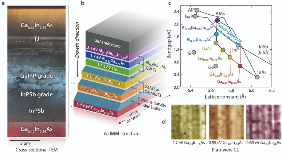
Figure 1: Researchers at NREL have produced a six-junction solar cell with record-breaking efficiency. The inverted metamorphic design features GaInP and InPSb grading layers (a), a variety of tunnel junctions (b), and the use of sub-cells with differing lattice constants (c). Scrutinising material quality with cathodoluminescence (d) revealed that threading dislocation densities are as low as around 106 cm-2 in each sub cell. Under one sun operation, the open-circuit voltage for the six-junction cell is 5.55 V, while the fill factor is 83.5 percent and the short-circuit current density is 8.46 mA cm-2. At 143 suns, the concentration that provides the highest efficiency, the open-circuit voltage increases to 6.29 V, the fill factor climbs to 87.2 percent and the short-circuit current density hits 1.23 A cm-2. Taken from Nature Energy J. Geisz et al. https://doi.org/10.1038/s41560-020-0598-5
In the summer of 2013 the triple-junction inverted meta-morphic cell briefly regained pole position. Success came from Sharp, producing a 44.4 percent efficient device at 302 suns.
From then on, record-breaking cells have had at least four junctions. French firm Soitec took the record from Solar Junction by drawing on expertise in wafer bonding. By uniting a pair of two-junction devices, designers could exploit far greater freedom in their choice of lattice constants for the cells. Refining this technology in partnership with researchers at the Fraunhofer Institute for Solar-Energy Systems, Germany, yielded a cell with 46 percent efficiency. Reported in late 2014, this record has stood for far, far longer than its predecessors.
Six-junction successes
To break this record, Geisz and co-workers have returned to the inverted metamorphic design, but upped the number of junctions to six. Helping their success has been their previous work on a four-junction device, formed by replacing a single InGaAs cell with a pair of them. This modification produced an efficiency of 45.6 percent at 690 suns, just below the record realised with the wafer-bonded cell.
Although Geisz has had much success with the inverted metamorphic over many years, he is not dismissive of alternative approaches. He views the dilute nitrides as very promising but challenging, having spent much time at around the turn of the millennia trying to make high-performance devices that incorporated this material system. However, he never enjoyed significant success with dilute nitrides. “At least by MOCVD, we haven’t been able to get as good a quality as we have with the metamorphic InGaAs. Solar Junction had a lot of good success, but they were growing that by MBE.”
The other approach that has produced record-breaking cells in recent times, wafer bonding, also has much merit, according to Geisz. “When we started the six-junction project, wafer bonding was one of the avenues that we would have liked to investigate. It’s really promising.”
But there is a price to pay for the freedom of design associated with wafer-bonding – relatively high costs, resulting from the need for twice as many growths and twice as many substrates.
Having started with an inverted metamorphic with three junctions and then moved on to designs with four, it may seem that progressing to five would be the logical way forward. But it’s not, argues Geisz: “We got the most bang for our buck working on six junctions directly. The six junction is kind of a natural sweet spot.”
Fabrication of NREL’s record-breaking cells began by loading GaAs substrates into an MOCVD chamber and growing 140 layers. This takes about seven-and-a-half hours, compared with just 3 hours for the original three-junction variant that has about 60 layers. Note that MOCVD is preferred to the other common approach for depositing these layers, MBE, because the growth recipe scales well, growth rates are higher, and it is easier to introduce sources into the chamber for all the layers and their dopants.
Growth of the six-junction structure begins with lattice-matched cells of Al0.18Ga0.33In0.49P (2.1 eV) and Al0.23Ga0.77As
(1.7 eV). They replace the single GaInP cell found in a three- or four-junction device. After that comes GaAs, the only binary cell. “It’s really a good material, so whenever possible, we like to use gallium arsenide”, explains Geisz.
The most radical change comes next. Rather than using just a single junction to collect all the low-energy photons, three are employed, separated by compositionally graded buffers. The justification for this, according to Geisz, is that there is a significant proportion of the sun’s radiation in the infra-red region.
To produce the buffers between the three cells – they are made of Ga0.84In0.16As (1.2 eV), Ga0.68In0.34As (0.95 eV), and Ga0.42In0.58As (0.69 eV) – metamorphic concepts are pushed to the limit. “We are grading it out beyond the lattice constant of indium phosphide,” says Geisz. “We’re using about 4.2 percent lattice mismatch.”
Buffers: arsenides vs phosphides
When Geisz and his co-workers started developing their six-junction cells, they used AlGaInAs for the grading layers. More recently, they have switched to GaInP, which yields better properties for the bottom junctions.
“Using phosphides is expensive and hard on the reactors,” warns Geisz, but he says that this must be weighed against their good properties. “The ordering in gallium indium phosphide tends to stabilise phase separation, and give some preferential glide to the dislocations.”
Due to this, dislocations are confined to the inactive regions, boosting efficiency. Benefits are seen when scrutinising the material with transmission electron microscopy and cathodoluminescence, techniques revealing that the typical threading dislocation density in the sub cell is 106 cm-2.
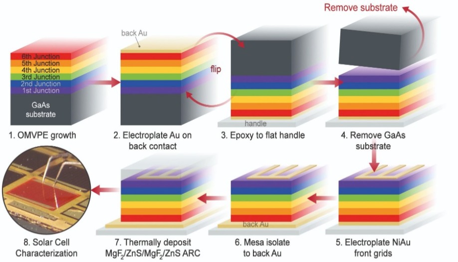
Figure 2: Fabrication of the six-junction solar cell begins with the epitaxial growth of a semiconductor stack, and then the deposition of a gold film. After bonding this gold layer to a handle substrate, the substrate is removed, before adding grids and an anti-reflection coating. Taken from J. Geisz et al. Nature Energy https://doi.org/10.1038/s41560-020-0598-5
Measurements on NREL’s record-breaking six-junction devices show that efficiency peaks at 47.1 percent at 143 suns. At higher concentrations, reductions are modest, dropping to a still impressive 44.9 percent at 1,116 suns. By tweaking the design, Geisz and co-workers also produced a device for maximum efficiency at 1 sun. Featuring a third sub-cell made from Al0.03Ga0.97As rather than GaAs, it produced an efficiency of 39.2 percent. Although that’s better than the previous high of 38.8 percent for a five-junction bonded cell, it does not make it into the record books, as qualification requires a minimum size for the cell of 1 cm by 1 cm.
While the obvious fit for this six-junction photovoltaic is at the heart of a concentrating system that sets new benchmarks for efficiency and power generation per unit area, it is also a very attractive candidate in unmanned aerial vehicles, where its excellent power-to-weight ratio is a massive asset.
Another market for the multi-junction cell is in space, generating power for satellites. To ensure that the latest NREL device performed at its best in this application, modifications would be required to the compositions and thickness of all six cells. But even if those changes were optimised, there would still be concerns related to radiation hardness.
“In general, the arsenides are not as radiation hard as the phosphide materials,” says Geisz, who has used a ternary arsenide, InGaAs, in the metamorphic junctions of the team’s record-breaking cells.
To see if this could be a show-stopper, the researchers are now starting to look into radiation hardness issues. “It’s not clear what the biggest issue for radiation hardness is,” admits Geisz, who says that investigations will begin by considering the impact of dislocations in the device.
Another goal for the team is to trim the resistance of their six-junction cell. It’s currently around ten times that of its three- and four-junction cousins, due to more pronounced zinc diffusion, resulting from longer growth times and higher growth temperatures; and the relatively high proportion of aluminium in the top sub-cell, which reduces carrier mobility, leading to an increase in resistance between the grids.
Hitting 50 percent
If the resistance of the six-junction design could be reduced to around 0.15 Ω cm2, the value realised in cells with fewer junctions, efficiency should increase to beyond 50 percent. In addition, the peak of the efficiency should shift to a higher concentration. This means that even without increasing material quality, efficiency could exceed 50 percent at 1000 suns.
The combination of record-breaking efficiency and a clear pathway to even better performance will pique the interest of makers of multi-junction cells all over the world. Fortunately, NREL is very open to working with cell manufacturers.
“We have been pretty straightforward about putting the technology into open literature, so we are hopeful someone will use it,” says Geisz. “We are funded by the US Department of Energy and we are looking to develop this technology for the good of all.”
While exceeding an efficiency of 50 percent would be a substantial milestone for a multi-junction cell, it’s by no means the limit of what may be possible. Even conservative calculations suggest that the upper bound for efficiency is as high as 62 percent, realised with a concentration of 1000 suns.
Closing in on this is by no means the only target for the team. One of its near-term goals is to bring down the cost of these devices, so III-V solar cells can compete with silicon technology. This is a substantial challenge, but the inverted metamorphic has the upper hand in one regard – it allows re-use of the substrate, a promising option for cutting material costs. “We are also looking at simplifying the very high efficiency structures,” adds Geisz, explaining that this offers another route to making high efficiencies more affordable.
Efforts at developing a six-junction cell at the NREL in Golden, CO, have been led by John Geisz (left), Principle Scientist in the High Efficiency Crystalline Photovoltaics Group. A key member of the team is Ryan France (right).
Credit: Dennis Schroeder, NREL.

Researchers at the International Reliability Physics Symposium highlighted the merits of RF operating life tests of GaN MMICs, the dangers of atomic migration in GaN HEMTs, and how small changes to the thickness of the barrier can have a dramatic effect on device performance
BY RICHARD STEVENSON
GaN is great material for making RF devices. Thanks to attributes that include its ability to operate at a high power density and a high efficiency, it is being deployed in 5G infrastructure, satellite communication and a variety of sensing, targeting and counter-measure applications.
For all these uses, reliability in paramount. In some cases it is critical to providing a satisfactory level of service, while in other circumstances lives depend on it.
Due to this state of affairs, studies of GaN reliability are ongoing, with several recent efforts having just been reported at the IEEE International Reliability Physics Symposium. The intention had been to hold the 58th annual meeting in this series in Texas, in late March and early April. But due to the Covid-19 pandemic, the conference moved on line (delegates could access prepared talks from 28 April until 30 May).
Virtual presentations discussing the reliability of GaN devices in the RF domain included: an account of the virtues of RF operational tests for GaN MMICs; a talk on the dangers of atomic migration of oxygen; and a presentation outlining why increasing the thickness of the AlN barrier can make such a difference to HEMT reliability. Read on to discover the insights from all three papers.
MMICs: DC or RF tests?
For the last sixty years or so, the dominant approach to evaluating the operational lifetime of a MMIC has been a DC accelerated lifetime test of the components. Within every MMIC there are transistors, diodes, capacitors, resistors and metallic interconnects, and each can be evaluated for its failure mechanisms under a DC test. Armed with the knowledge that this brings, it is possible to predict the lifetime of the circuit.
But while this approach is valuable, it has its flaws says Qorvo’s Elias Reese. He posed the question: “What is it that derives the need for something beyond the DC life test?” The answer, according to him, is the RF stresses on GaN circuits.
Although these stresses are not found in many other forms of IC, where signal levels are typically microwatts or milliwatts, they are present in GaN MMICs, where power levels can extend to the kilowatt range. When these MMICs are well-designed, they offer a compact, efficient source of RF power.
To do so, there is an impedance transformation on the chip that enables the RF voltage to great exceed the bias voltage provided. For a high-power amplifier MMIC made from GaN, the bias can be 65 V, while the voltage at the output port can approach 1000 V, creating significant stress.
Stress can also be found in the interconnects. RF signals are not uniformly distributed through the cross-section of a conductive line, but are concentrated at the edges. So, in extreme cases, it is even possible that a line that is not passing any DC current can still fail, due to RF current alone.
Simulating the RF fields in a MMIC is not an easy task. As the components within this circuit have dimensions comparable to the wavelength of the output signal, there are significant variations in electromagnetic field across these building blocks.
“So you have to divide this up into thousands of pieces to accurately calculate the RF voltages and currents across the entire circuit,” says Reese. “That’s a very complex problem, and frankly takes hours and hours of time to solve.”
A preferable alternative, says Reese, is the RF operating life test, which is an approach that dates back around 40 years. He detailed an example of this: 24 MMIC high-power amplifiers tested simultaneously for 2000 hours, using prescribed stress conditions and in situ monitoring of key electrical and thermal parameters (see Figure 1).
Although a speedier test is desirable, it is far more complex, warned Reese: “When you try and use accelerating factors such as temperature, you no longer have the ability to hold other factors, such as voltage and current, constant.”
The conclusion to draw is that while RF operating life tests take much time, they provide a level of insight that is not found by other, quicker approaches.
Figure 1. Engineers at Qorvo have conducted simultaneous RF operating lifetime tests on 24 MMIC high-power amplifiers, using independent bias supplies, controls and RF signals.
Scrutinising HEMTs
Efforts at evaluating the reliability of HEMTs with a variety of gate lengths were discussed in a talk given by Enrico Zanoni from the University of Padova. He is working on a variety of European projects, included one that runs from this year until 2023 and is entitled Empowering GaN-on-SiC and GaN-on-Silicon technologies and the next challenging millimetre-wave applications.
In Zanoni’s presentation, he detailed a study of a portfolio of devices made by a collaboration between the team at the University of Padova and colleagues at the IMWS Fraunhofer Institute Halle. The partnership’s investigation included transistors with a gate length of 0.5 µm that could be used for frequencies up to 6 GHz, variants with 0.25 µm gate lengths that can operate at 20-30 GHz, and those with 0.15 µm gate lengths that provide low-noise amplification between 30 GHz and 50 GHz.
Zanoni and co-workers have undertaken extensive testing on their portfolio of devices. Studies have included: 24 hour short-term tests, followed by microscopy, to identify issues related to inter-diffusion; measurements lasting between 500 hours and 4000 hours that consider the impact of elevated temperatures on key electrical characteristics; and an investigation into the impact of carbon-doping levels on short-channel effects in HEMTs with short gate lengths.
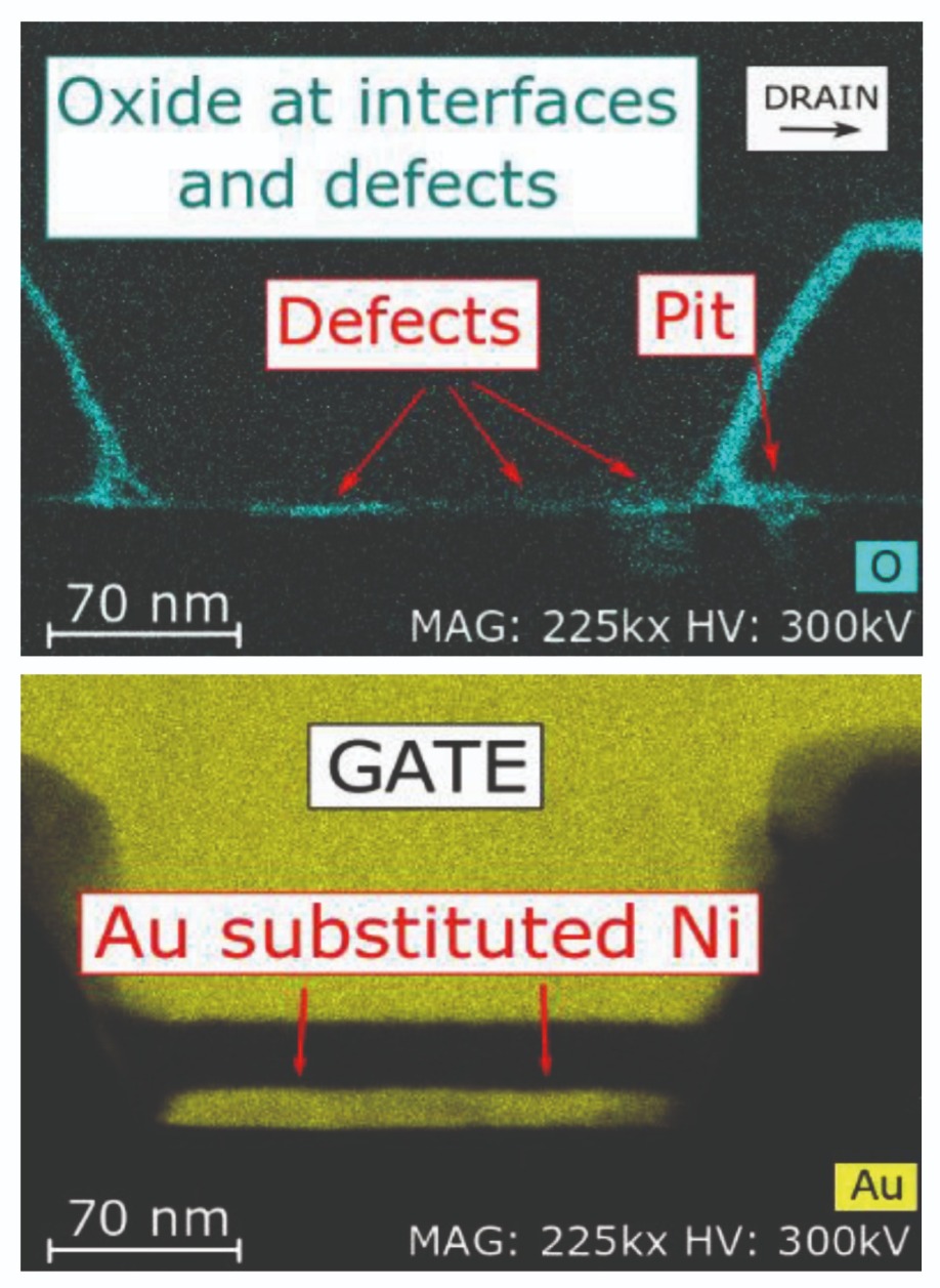
Figure 2. Energy-dispersive X-ray analysis by a team from the University of Padova and IMWS Fraunhofer Institute Halle revealed inter-diffusion issues in first-generation HEMTs. In these transistors, operation at elevated temperatures led to oxygen diffusion under the AlGaN Schottky contact (top) and complete substitution of gold for nickel in the Schottky contact. Gold forms a uniform thick layer.
To identify what is happening within the HEMTs during degradation, the team took the devices, created cross-sections by ion-beam milling, and scrutinised the samples with scanning electron microscopy, transmission electron microscopy and energy-dispersive X-ray analysis. This revealed that gold gradually substituted for nickel in the Schottky contact, and oxygen also caused issues, promoting AlGaN oxidation and pitting.
Second-generation devices have addressed these short-comings by using a different gate metallisation scheme and double-layer passivation. These HEMTs exhibit far smaller changes to transconductance at junction temperatures of up to 250 °C, a result that has led Zanoni to view this as a “pretty robust technology”.
The team have conducted long-term thermal storage tests on this second-generation technology, with HEMTs with 0.5 µm and 0.25 µm gate lengths heated to either 300 °C, 325 °C or 350 °C for 4000 hours. These tests identified a positive threshold shift of 0.2-0.25 V, and a change in Schottky barrier height from 0.84 eV to 0.58 eV followed by recovery to the initial value. The shift in barrier height led to an increase in gate leakage current by one-to-two orders of magnitude; this recovered with a reduction in device temperature.
Further evidence of robustness at elevated temperatures came from DC life tests on these devices, using a range of conditions that included channel temperatures up to 355 °C, drain currents up to 0.3 A/mm and drain source voltages up to 100 V. These conditions produce degradations of below 10 percent in drain current and transconductance.
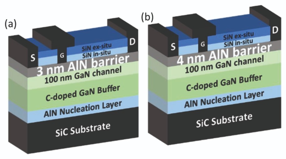
Figure 3. Engineers at Institute of Electronics, Microelectronics and Nanotechnology (IEMN) at Villeneuve d’Ascq, France have compared the performance of HEMTs with 3 nm-thick and 4 nm-thick barriers.
For HEMTs with a gate length of 0.15 µm or below, short-channel effects can arise that threaten to exacerbate drain-source leakage and shorten device reliability. Strategies for success include adding back-barriers, doping with either carbon or a combination of carbon and iron, and using N-polar AlGaN/GaN channels.
Zanoni and co-workers have considered five different forms of 0.15 mm gate length HEMT. All these devices were made using the same process, the same batch, on epitaxial layers from three different suppliers. For all the samples, peak iron concentration is nominally 2 x 1018 cm-3, while the carbon concentration is either 2 x 1016 cm-3 or 8 x 1016 cm-3.
“Devices with high carbon doping tend to be better,” concluded Zanoni. Current degradation during off-state and on-state stress tests is lower. However, a 24 hour on-wafer test shows that co-doped devices have an inferior performance and reliability to those doped with just iron.
Better barriers
Investigations of the reliability of GaN HEMTs with even shorter gate lengths have been undertaken by a team from the Institute of Electronics, Microelectronics and Nanotechnology (IEMN) at Villeneuve d’Ascq, France. This effort is highly valued, due to the paucity of reliability studies on millimetre-wave GaN devices. The key finding in this study is that the thickness of the barrier, which is highly strained, can govern device reliability.
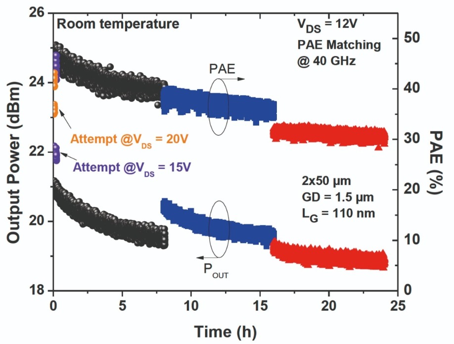
Figure 4. GaN HEMTs with 4 nm-thick barriers show significant degradation in output power and power-added efficiency during a 24 hour stress test.
Fabrication of HEMTs involved processing epiwafers produced by MOCVD and provided by EpiGaN-Soitec.
These epiwafers, grown on 4-inch SiC substrates, consisted of an AlN nucleation layer, a 1 µm-thick carbon-doped GaN buffer, a 100 nm-thick GaN channel, an AlN barrier either 3 nm- or 4 nm-thick, and a 10 nm-thick SiN passivation layer. The latter, added in-situ, provides passivation and reduces surface states.
To create HEMTs from these epiwafers, Kabouche and co-workers etched the SiN layer, before adding Ti/Al/Ni/Au source and drain contacts and an asymmetric self-aligned Ni/Au T-gate (see Figure 3).
Measurements of power performance at 40 GHz were conducted on 2 x 50 µm HEMTs. For the transistors with a 4 nm barrier, an increase in drain-source voltage from 10 V to 20 V led to a fall in power-added efficiency from 50 percent to 45 percent, attributed to device degradation. In comparison, the variant with the 3 nm-thick barrier realised a power-added efficiency of 50 percent at 10 V, and 48 percent at 30 V.
Kabouche and co-workers subjected both types of device to a 24 hour stress test, using a drain-source voltage of 12 V and 8 hour steps, after which the gate voltage is adjusted to maintain a 100 mA/mm drain current. During the course of the test, the power-added efficiency of the HEMT with a 4 nm-thick barrier fell from 45 percent to 30 percent, while the variant with the 3 nm-thick barrier showed no degradation.
In order to further assess the robustness of this structure, the team also performed short-term wafer RF stress tests at baseplate temperatures of up to 140 °C, which correspond to a channel temperature of more than 250 °C. The HEMT with the 3 nm-thick barrier was fully stable at a drain-source voltage of 20 V, but at 30 V significant degradation took place, causing the power-added efficiency to fall from 50 percent to 30 percent. The benefits wrought from reducing the barrier thickness from 4 nm to 3 nm may raise a few eyebrows, given that the critical thickness for an AlN layer grown on GaN is only about 1 nm. However, the team points out that this thickness can be increased to 2-3 nm with a “proper” in-situ cap. This leads to a lower defect density, allowing a HEMT with a 3 nm-thick barrier to withstand a higher electric field and elevated temperatures.
Kabouche revealed that one of the goals for the team is to investigate how the quality of the barrier varies with its thickness. The researchers are also planning to carry out additional on-wafer RF stress tests at 40 GHz, where they do not adjust the gate bias voltage before each step, so that they can observe the impact that this has on the output power density and power-added efficiency. Other intentions are to evaluate larger devices, such as those with dimensions of 4 x 50 µm and 6 x 50 µm, and benchmark other aluminium-rich ultrathin barriers, such as InAlGaN.
Progress by this team from IEMN, as well as that by researchers at Qorvo and the University of Padova, could be reported at next year’s International Reliability Physics Symposium. By then, hopefully the Covid-19 pandemic will be over, allowing experts in device reliability to meet at the Hyatt Regency in Monterey from 21-25 March 2021.

Fluidic assembly of GaN microLEDs yields low-cost displays with better performance, efficiency and lifetime than those made with LCDs and OLEDs
BY PAUL SCHUELE, KURT ULMER, KENJI SASAKI AND JONG-JAN LEE FROM ELUX
MicroLED displays are made by integrating two mature, multi-billion dollar technologies. One is the GaN LED, developed for general lighting; and the other is the large-area, active-matrix backplane, developed for LCD and OLED displays.
The manufacture of a microLED display involves making LEDs with diameters of just 5 µm to 100 µm and using them to form the subpixels that provide direct emission. Compared with LCD displays, this mode of operation provides a far higher efficiency, alongside a very high contrast – it is over 50,000:1. The technology also outperforms OLED displays, which suffer burn-in effects and cannot realise as high a brightness.
Market penetration of microLED displays is tipped to begin with: large information displays that require high brightness; home theatre applications, which will benefit from increased dynamic range; and automotive displays, as they place a premium on high contrast and reliability.
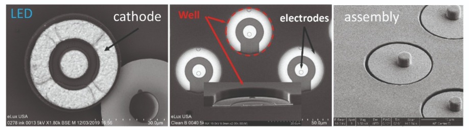
Figure 1. Scanning electron microscope images of: 40 µm microLEDs (left), matching electrode and well structures on a display substrate (centre), and assembled cells (right). The central image shows matching electrodes on the display backplane, and the cylindrical trap structure used to capture a microLED.
A very promising alternative, tackling all these challenges, is a massively parallel fluidic assembly process developed by our team at eLux of Vancouver, WA. The technology we are pioneering positions each microLED by capturing it in a trapping structure, which contains the electrodes connected to the display control circuitry.
Typically, our process begins with microLEDs emitting at 450 nm, that are 40 µm in diameter and have a thickness of about 4 µm (see Figure 1 for typical scanning electron microscope images of these flat disc-shaped structures). These microLEDs, fabricated from conventional GaN-based blue LED wafers, are flip chips featuring anode and cathode electrodes on the same surface, arranged as concentric rings. By using a low-temperature solder for the electrodes on the microLED, we connect them to substrate electrodes by an annealing process that takes place after fluidic assembly (see right image in Figure 1, showing the display after assembly, with microLEDs populating each of the assembly sites).
The binning challenge
The microLEDs we deploy in our microLED displays are fabricated from wafers that are like those used for general lighting. The advantage of this approach is that the cost-per-device is very low – but it also introduces problems unique to microLED technology.
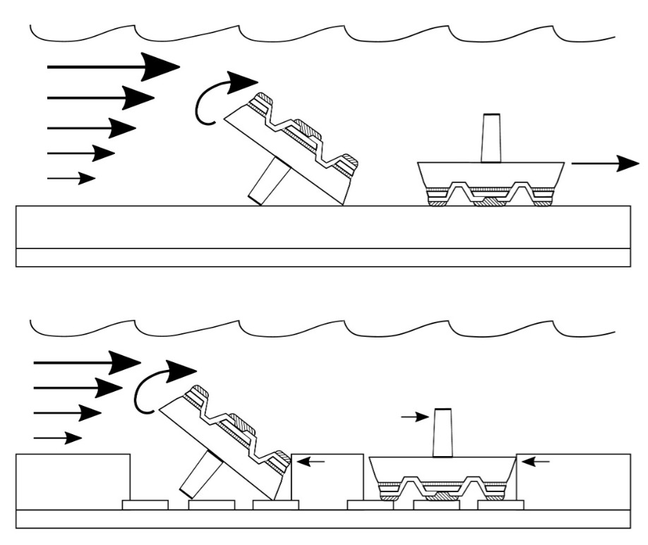
Figure 2. During microLED fluidic assembly, post-down orientations are unstable, due to the parabolic fluid velocity profile at the display panel surface.
For microLEDs, this modus operandi is an issue. Even in the most expensive, state-of-the-art microLED fabs, defectivity levels are still 0.1 percent or more. The imperfections result in dark sub-pixels, which are unacceptable in display products.
Unfortunately, it is impractical to identify and discard defective microLEDs using a binning process. Handling and functional testing these tiny devices is difficult, due to their diminutive size, their lack of packaging and the incorporation of electrodes. With a UHD display requiring at least 24.8 million microLEDs, testing times are too long to be practical. What is needed are new structures and methods that prevent defective microLEDs from ruining displays with defective subpixels.
To meet this challenge, our production process begins by mapping the defects on the microLED wafer. A variety of methods can accomplish this, including optical inspection, micro-photoluminescence, electroluminescence and cathodoluminescence. Armed with this mapping data, it is a simple matter to selectively harvest the good microLEDs. They form part of an ink used in our fluidic assembly process, while defective devices are discarded. Making displays from only known good microLEDs is one of the unique advantages of the fluidic assembly method.
Fluidic assembly
Our fluidic assembly process allows us to pass a liquid suspension of millions of microLEDs over a substrate that is populated with an array of trap sites, arranged as display pixels. As the microLEDs are similar in size to red blood cells, many of the suspension handling methods are like those used to handle biological samples. Once the microLEDs have settled, the suspension is forced to flow across the substrate, pushing devices across the surface and over the trap sites. Many assembly attempts occur randomly every second, thanks to numerous microLEDs and trap sites. Thus, stochastic assembly is massively parallel, and proceeds very quickly compared with competing deterministic assembly processes, where speed is limited by the mechanical characteristics of a pick-and-place head, or the mass transfer stamp.
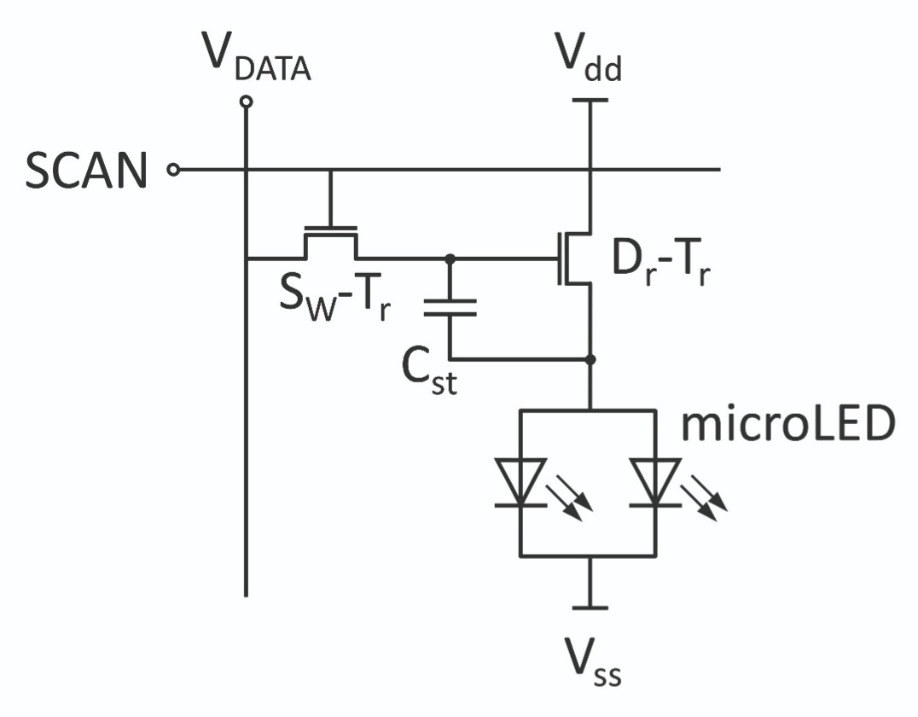
Figure 3. A two-transistor TFT circuit for a display sub-pixel.
To ensure that fluidic assembly is a success, most assembly attempts should employ the correct orientation of the LED, and make sure that once a device is trapped, it must never escape. The likelihood of these occurrences is increased by engineering the shapes of the trap structures and the microLEDs, which feature a protruding post. This ensures that during fluid flow desired orientations and positions are stable, while undesirable configurations are unstable.
One important consideration is the fluid velocity. As this decreases parabolically to zero at the display surface, the microLEDs that are pushed along by the flowing fluid are subjected to a varying force that increases with height. Consequently, microLEDs that have their protruding post facing downwards tend to flip over to a post-up orientation, which has lower applied force (see Figure 2, upper left). This means that after a short time, all microLEDs on the surface are in a post-up orientation.
A second line of defence is that even if a post-down device is captured by a well (see Figure 2, lower left), there is a significant cross-sectional area exposed to fluid flow. This will cause the mis-oriented microLED to flip out of the well, settle to the surface post-up, and then assemble in another open well somewhere down stream.
It is critical that the trap sites are a good fit for the shape of the microLEDs, as this ensures that most assembly attempts result in a microLED falling into a trap and stopping (see Figure 2, lower right). We accomplish this with cylindrical wells that are slightly larger than the diameter of the microLED discs and deeper than their thickness. Depth is essential, minimising the de-trapping force on an assembled microLED and allowing other microLEDs to flow over it.
Making displays
We make our microLED displays on a glass substrate, using an array of thin-film transistors (TFTs) to control the current to each LED. The sub-pixel circuit has an access gate and a current-control transistor that drives two microLEDs in parallel, with the current set by the charge stored on the storage capacitor (see Figure 3). By using two-fold redundancy, we can compensate for one unconnected microLED – in that case, all current passes through one device, producing a similar amount of light to two devices in parallel.
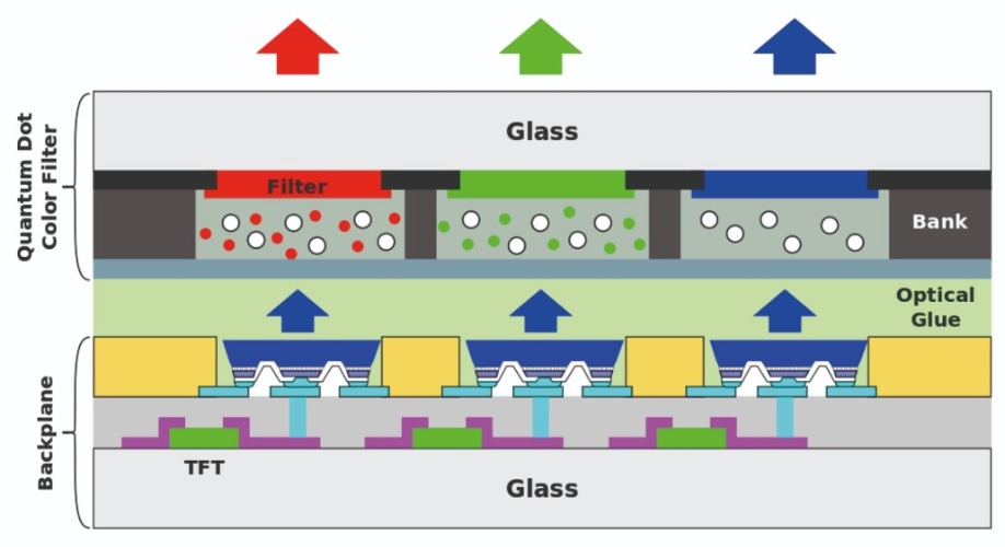
Figure 4. Red, green and blue pixels are formed by combining blue-emitting devices with quantum-dot phosphors.
To produce an RGB pixel, we use an optically transparent glue to laminate the display backplane containing TFT control circuits and the assembled blue microLEDs to a quantum-dot colour filter sheet (see Figure 4). Two features of the quantum-dot colour filter glass are: a structure set by the black matrix and bank material that prevents photons from travelling between adjacent pixels; and a form that defines the printed quantum-dot layer. The quantum dots are key to the operation of red and green pixels, which produce their colour by absorbing blue emission and re-emitting at longer wavelengths. For blue sub-pixels, the printed material scatters the blue light from the microLEDs, to replicate the isotropic distribution of light emitted from the quantum dots.
The conversion efficiency of the red and green quantum dots is about 60 percent, so to meet the desired colour temperature, the white point of the display is adjusted to 6500 K by decreasing the intensity of the blue sub-pixels (see Figure 5). The display has a colour gamut area 116 percent of NTSC and the white point matches D65 (see Figure 6). By further tuning the quantum dot colour filter, we can extend the colour gamut. A pixel-by-pixel mura correction can adjust the intensity and colour balance of each pixel.
Multiple market opportunities
MicroLED displays offer several advantages over current display technologies, including a far higher brightness, high contrast, a wide colour gamut and high reliability. However, development is still at an early stage. For an overview see Table 1, which outlines the prospects for microLED displays in several different product categories, and also offers a rough estimate of the degree of difficulty and the amount of development still to be realised to make each one a success.
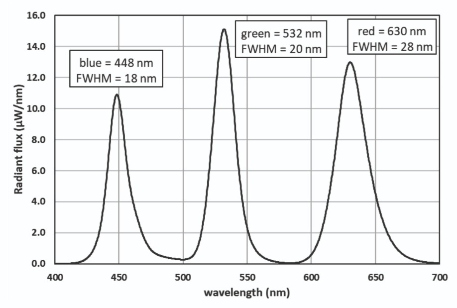
Figure 5. The white point spectrum of the eLux microLED display with a colour temperature of 6500K (D65).
An early implementation of microLEDs is in the very large public information display. The requirements for high brightness, no burn-in and large pixel size are ideally met, but prices today are astronomical, with costs exceeding $20k/m2. We believe our technology can be a game-changer, thanks to the very low-cost of fluidic assembly.
Virtual reality and augmented reality are very attractive markets for small size displays. Success is challenging, however, as to meet the requirement for very high resolution, microLEDs must be very small. When shrinking dimensions to below 10 µm LED efficiency plummets and the pixel sizes are too small for quantum dot colour conversion. Compounding the situation, it is unclear how to assemble three colour emitters to make an RGD display. Consequently yield, cost and heat dissipation are serious issues for VR/AR applications of microLEDs. Because it may not be possible to use fluidic assembly when microLEDs dimensions are below 5 µm, we are not planning to address VR/AR markets.
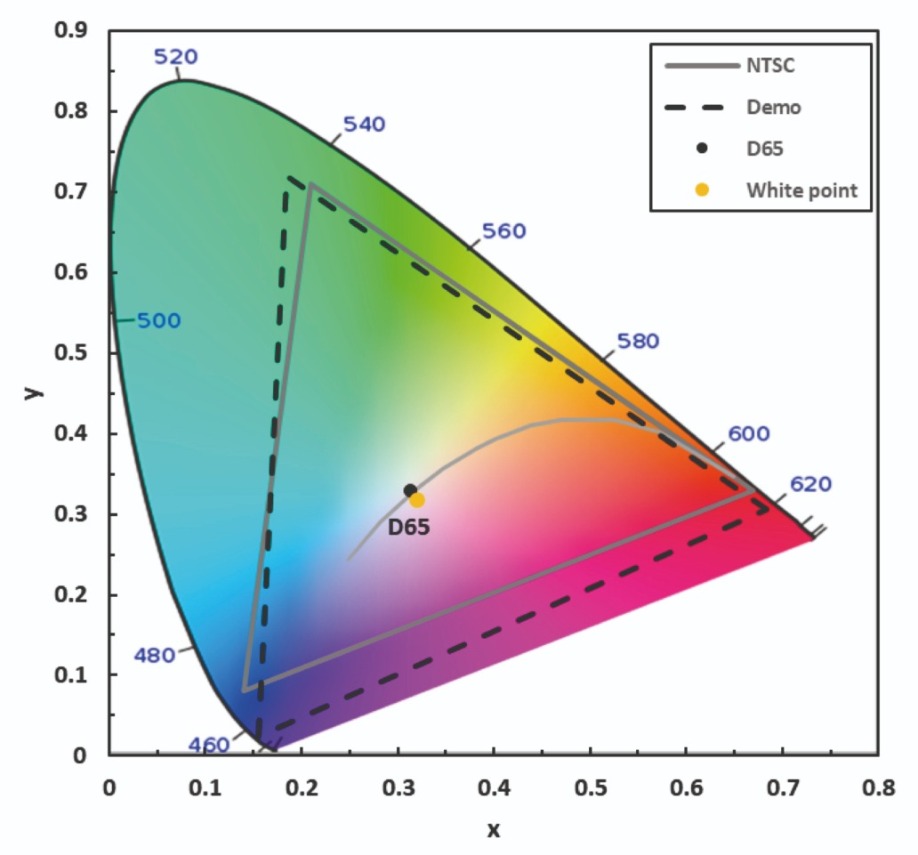
Figure 6. Colour gamut of the eLux microLED display showing 116 percent of the NTSC gamut and a white point set to D65.
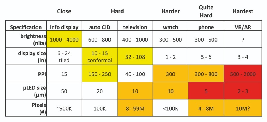
Table 1. Properties of microLED displays for different products. Cell colour represents level of difficulty to realise the required performance. Clear cells are achievable now, yellow will be difficult, orange extremely difficult and red is hard to imagine.
Another opportunity is to switch from using colour-converters to direct-emitting LEDs, with blue and green GaN emitters joined with red-emitting, AlGaInP microLEDs that are assembled in the same way. We are looking forward to the future, given the great promise that the combination of microLEDs and fluidic assembly technology has for revolutionising the low-cost manufacture of displays for a wide range of products.
M. Boncheva et al. MRS Bulletin 30 736 (2005)
K. Ding et al. Appl. Sci. 9 1206 (2019)
T. Wu et al. Appl. Sci. 8 1557 (2018)

A wafer-scale wave of precisely controlled electrons delivers atomically smooth, damage-free etching
BY SAMIR ANZ, DAVID MARGOLESE, STEWART SANDO AND WILLIAM A. GODDARD III FROM VELVETCH
THE MARKETS for compound semiconductor devices have grown rapidly over the last decade and are forecast to accelerate in the coming years. Driving this growth are the increasing demands for devices that deliver higher performance, higher output power, higher operating temperature and higher efficiency in a wide variety of applications, including: 5G wireless networks, satellite communications, military radar, EV motor control, EV charging stations, industrial control, solid-state lighting and optical quantum well devices.
Those working in the compound semiconductor industry need to continue to advance device fabrication, so that these rapidly advancing applications are served by products with improved capabilities. Increases are needed in switching speeds, operating voltages, breakdown voltages, leakage currents, quantum well efficiencies, Q factors and power efficiencies, so that the technical requirements are met in various applications.
One way for compound semiconductor manufacturers to deliver on this front is to turn to new wafer fabrication technologies that provide even tighter control over critical device parameters. By switching to superior processes, these chipmakers can fabricate surfaces, interfaces, lattice structures and circuit elements that get far closer to ideal compound semiconductor device designs.
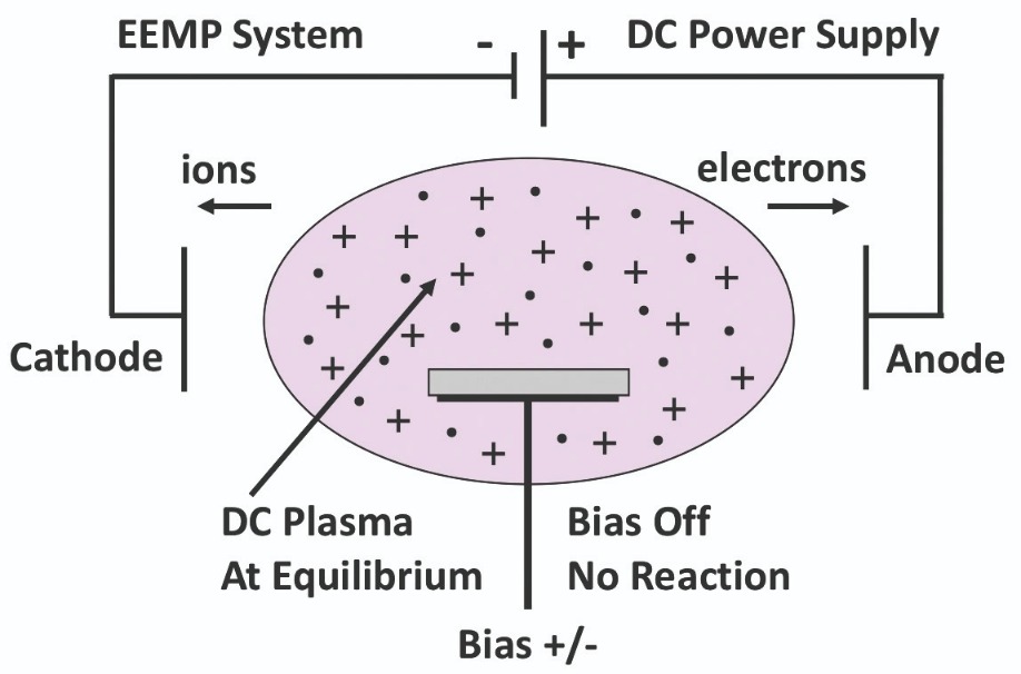
Figure 1. Electron-enhanced material processing begins by generating a room-temperature argon plasma, formed by the flow of a direct current between the cathode and anode. The bias signal is generated separately and is connected to the wafer stage.
Since the introduction of plasma etching in the 1970s, etching technologies have steadily advanced. The two most prominent are reactive-ion etching and atomic-layer etching. Both bombard the surface with ions – in one case, it’s reactive ions; and in the other, it’s argon ions. Neither option is ideal, because the ions that bombard the surface can damage the crystalline structure, which may be further impaired by exposure to elevated processing temperatures.
Etching with electrons
Addressing these conditions is an electron-enhanced material processing technology that we have developed at Velvetch, a start-up based in Pasadena, California, that has teamed with PVATepLa America to manufacture and support the systems. Our process is based on a fundamentally different etch mechanism, utilising a room-temperature DC plasma to produce wafer-scale waves of precisely controlled electrons. These electrons stimulate an excited-state etch reaction across the entire surface of the material.
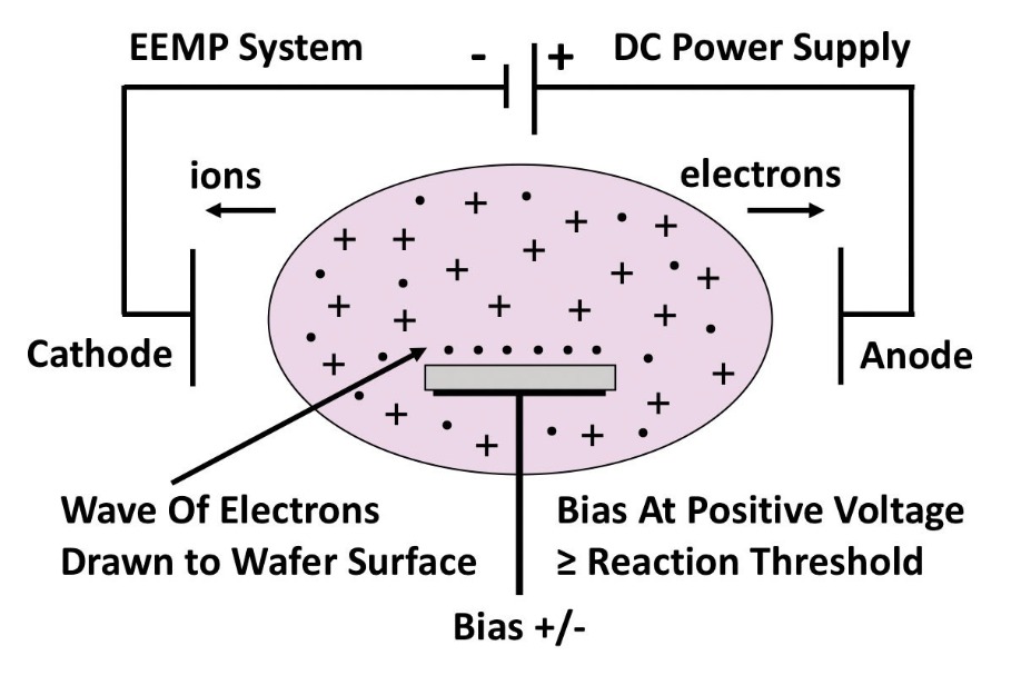
Figure 2. In an electron-enhanced material processing tool, a wave of precisely controlled electrons is drawn to a sample that is held on the wafer stage when the bias signal is driven positive to a voltage equal to or greater than the desired excited state reaction threshold.
Etching begins by mounting a wafer on a stage immersed in an equipotential, positive column of a DC plasma (see Figure 1). To maintain the plasma, a low-voltage DC current is directed through electrodes outside the wafer-stage zone. In the absence of an etch bias, electrons in the DC plasma equilibrate to the uniform plasma potential. The etch is initiated by applying a positive etch bias to the wafer stage. This draws down a dense wave of precisely controlled electrons to the surface of the wafer with an energy equal to the difference between the DC plasma potential and the voltage of the etch bias (see Figure 2).
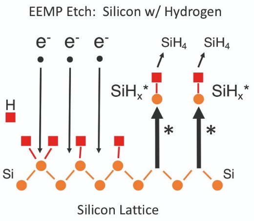
Figure 3. When using electron-enhanced material processing to etch silicon with hydrogen, the process begins with a wave of electrons arriving at the silicon lattice (see left side). After the reaction, excited state etch products depart the silicon lattice (see the right side).
A simple, illustrative demonstration of how electron-enhanced material processing works, and its unique capabilities, is the etching of silicon with hydrogen (see Figure 3). During this process, neutral hydrogen atoms form a loosely bound corrosion layer with the dangling bonds of the top atomic layer of silicon. Note, however, that hydrogen does not etch silicon until the next wave of electrons arrives with the positive-going etch bias. At this point, electrons directly couple their energy into the electron orbitals of the silicon atoms, and partially reacted etch products are raised to an excited energy state. The top layer of the silicon atoms is then instantly released from the lattice, and excited-state etch products are repelled from the silicon surface.
During this reaction, three excited-state etch products result from the reaction of silicon and hydrogen: SiH1*, SiH2* and SiH3*. The predominant product is SiH2*, because the top layer of a silicon lattice tends to present two dangling bonds to the vacuum.
All three forms of excited-state etch product react with hydrogen in the room-temperature argon plasma. This generates a SiH4 etch product, which drops back down to the ground state as it is pumped away by the etch system. As the excited state reaction proceeds, the temperature of the silicon wafer rises by no more than a couple of degrees.
Swap hydrogen for chlorine and atomic layer etching still proceeds in the same manner. Excited etch products are now SiCl*, SiCl2* and SiCl3*, and SiCl4 is the final etch product (see Figure 4).
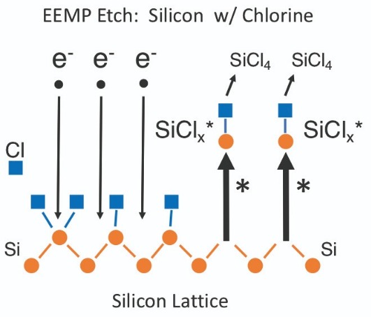
Figure 4. Etching silicon with chlorine via electron-enhanced material processing. A wave of electrons arrives at the silicon lattice (left side), and excited state etch products depart from this surface (right side).
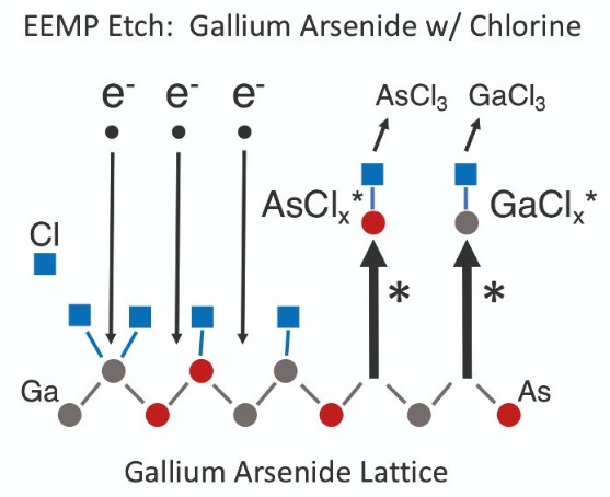
Figure 5. There are two excited-state reaction pathways for etching GaAs with chlorine by electron-enhanced material processing: one is for etching gallium with chlorine, and the other for etching arsenic with chlorine.
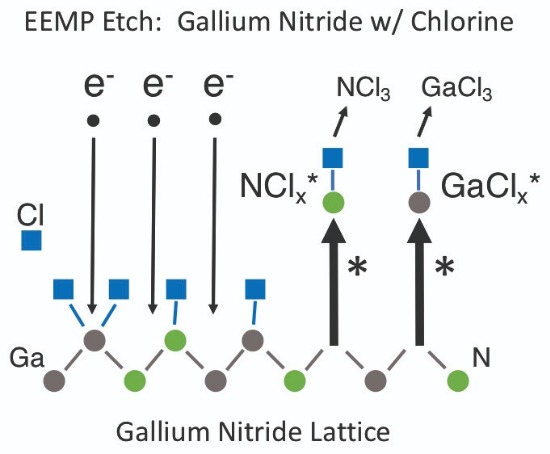
Figure 6. There are two excited state reaction pathways for the etching of GaN with chlorine by electron-enhanced material processing. The excited-state etch products for gallium are GaCl* and GaCl2*, and the excited-state etch products for nitrogen are NCl* and NCl2*. The final neutral etch products for GaN are GaCl3 and NCl3.
Using a standard plasma etch process gives a different result. When we applied plasma etching to a GaAs wafer – using a gentle reactive recipe with a mixture of SiCl4 and BCl3 as the reactant gases – raised shoulders appeared in an X-ray rocking curve. These features were not seen in the equivalent curve for an untouched GaAs wafer (see Figure 8), and prove that standard plasma etching alters the stoichiometry of the etched GaAs wafer, while it is retained with the electron-enhanced material process.
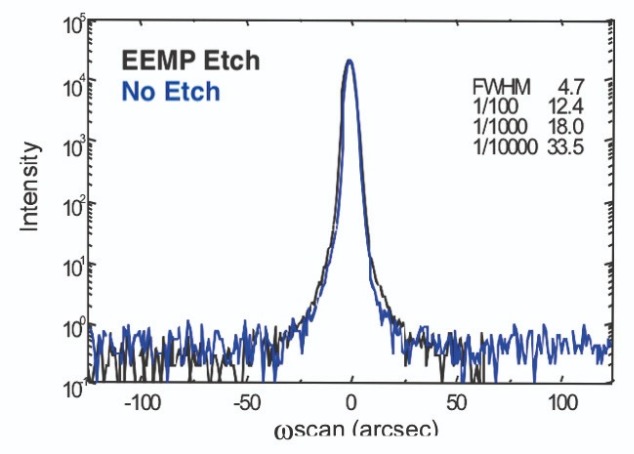
Figure 7. X-ray rocking curves provide a comparison of GaAs etched by electron-enhanced material processing (black) and unetched GaAs (blue). The two curves are almost identical, indicating etching did not alter the stoichiometry.
We have also applied our chlorine etch technology to the contact areas of GaN-on-sapphire diodes, working in partnership with a team at the University of California, Santa Barbara. This study involved etching through the 40 nm GaN cap to open a contact pattern on the p-GaN surface of a p-n diode (see Figure 9), before depositing a metal contact on the exposed p-GaN surface. This diode, formed using a 3 minute contact etch, had a turn-on voltage of approximately 6 V. In comparison, controls produced by reactive-ion etching had turn-on voltages in the 10 V to 12 V range. We attribute the superior turn-on voltage to our damage-free, stoichiometry preserving etch technology.
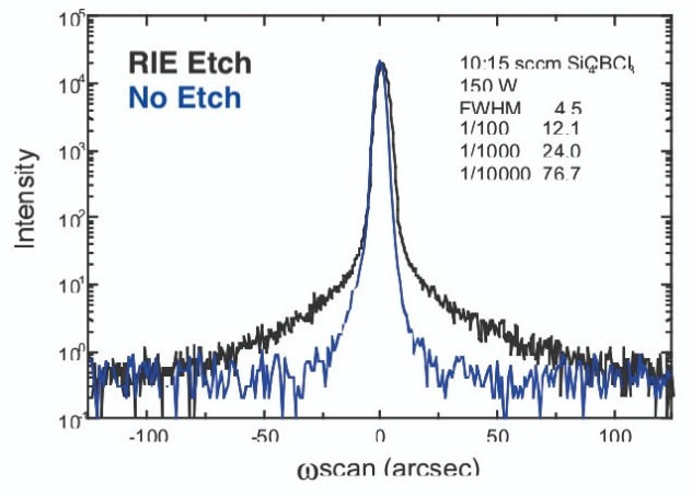
Figure 8. Compared to the X-ray rocking curve of unetched GaAs (blue), that subjected to reactive-ion etching (black) has elevated shoulders. This feature reveals that reactive-ion etching creates lattice damage to GaAs and alters its stoichiometry.
One of the more difficult challenges encountered when etching compound semiconductors is the damage-free removal of the growth substrate from an epitaxial stack containing quantum wells. This is a problem that we have worked on through a collaboration with VerLASE Technologies.
Our efforts involved removing a GaAs substrate from the bottom of a II-VI device containing ZnSe quantum wells, ZnCdSe barriers, and ZnSe optical window caps surrounding the active region. We began by mounting the ZnSe top cap of the II-VI on a temporary glass plate, flipping over the assembly (see Figure 11) and etching the GaAs substrate.
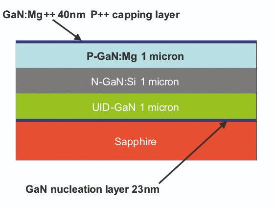
Figure 9. To make the contact to the p-GaN diode layer, etching is used to create an opening in the GaN p++ capping layer.
Previous efforts to remove the GaAs substrate with plasma etching had proved problematic, with ion bombardment generated by the plasma process damaging the ZnSe cap. Surface damage attenuated light entering the quantum well device, while deterioration of lattice quality diminished the Q factor of the quantum well, leading to a broadening of the spectral emission.
Thanks to the precision with which we control the electron energy during our etch, we were able to use our technology to remove the GaAs layer and make a hard stop on the ZnSe cap layer, without causing any damage. Employing a technique known as ‘special aperture plate’, we etched several test spots on the wafer. At every additional spot, we incrementally increased the electron energy, allowing us to characterize the etch threshold for the GaAs layer.
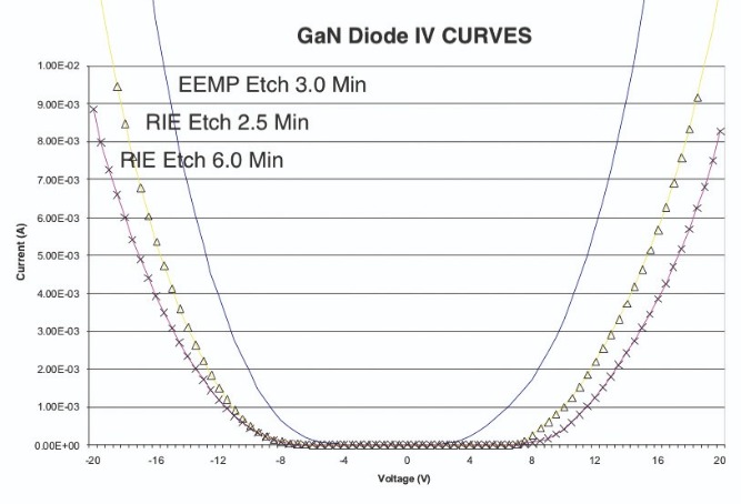
Figure 10. Current-voltage plots for GaN diodes, formed by etching the p-GaN contact, highlight the superiority of electron-enhanced material processing (blue trace) to reactive-ion etching (yellow triangles and pink crosses are for reactive-ion etching processes with a duration of 150 second and 6 minutes, respectively).
Researchers at VerLASE have found that the ZnSe cap associated with the quantum well device spots is as optically smooth as the original surface. Spectral analysis verifies that no damage has been imparted to the cubic zincblende lattice structure of the ZnSe cap layer.
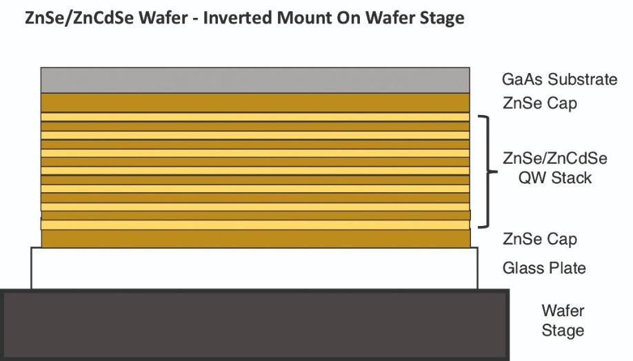
Figure 11. Electron-enhanced material processing enables damage-free removal of a GaAs growth substrate from an epistack containing a ZnSe/ZnCdSe quantum well device. To liberate the GaAs substrate, it is mounted to a glass plate, then inverted.
Projectors benefit from light engines that combine powerful blue and red LEDs with green sources based on phosphor pumping
BY ALEXANDER MARTIN FROM OSRAM OPTO SEMICONDUCTORS
IF YOU ATTEND fairs like this year’s Consumer Electronics Show in Las Vegas, you’ll know that if you want to deliver a presentation to your peers, you have plenty of viewing options available. The leading manufacturers are showcasing ever bigger, often scalable and even foldable screens, based on either OLED or micro-LED technologies.
Unfortunately, both these technologies have one major problem – the bigger the screens get, the more expensive they get. And for microLED-based technologies there is another sticking point – the challenge of affordable, high-throughput mass production, which the makers of these screens will try and tackle over the next few years.
While developments in screen technology have grabbed the headlines, progress in modern projection is often unnoticed. Many will have missed the strides that have been made to enable LED projection to become a viable alternative offering a higher brightness than conventional LCD and OLED screens. Gone are the days when you have to darken the meeting room so that the audience can view the presentation.
Another strength of the LED projector over LCD and OLED screens is its increased flexibility. With this technology, scalable picture sizes can be projected on any rigid or flexible surface, freeing up room space.
At Osram Opto Semiconductors of Regensburg, Germany, we are playing our part in the emergence of this class of projector, by developing and commercialising a new LED technology that allows projectors based on this light source to realise record-breaking brightness levels of more than 3,000 ANSI lumens. This level of brightness is suitable for large projection markets: projectors for office and home cinema use.
Our efforts offer makers of projectors a superior alternative to their incumbent source of lighting, the conventional, mercury-ridden, high-intensity discharge lamp. As demand for a brighter, more reliable source has grown, lasers emerged as the logical successor. And more recently, improvements to the performance of the laser have positioned them as a high-quality, sophisticated alternative to mercury vapor lamp. Strengthening their case is their long lifespan and brightness levels that do not diminish over time, which is another weakness associated with conventional lighting technology.
As lasers have emerged as promising candidates, LEDs have started to offer a competitive alternative. Initial success for the LED-based projector came a few years ago, with the introduction of the first pico projectors. They produced just 15 lm, a small fraction of the 4000 lm provided by today’s LED-based projectors. As well as producing a great deal light, LEDs – and for that matter, lasers – take up very little space, an attribute highly valued by designers of projectors.
Mercury lamps versus LEDs
One way to judge the quality of an image is to consider its range of colours. Conventional projectors typically use a white-light source, with primary colours generated through a mechanically-driven colour wheel. Due to the mechanical moving component and the large size of the high-intensity discharge lamps, these projectors require a relatively large light engine architecture. In addition, they are not that robust.
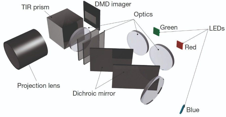
A projector system with a digital micromirror device and single red, green and blue LED chips
With LEDs, there are many benefits. They are more compact, they have a longer lifetime, they provide comparable brightness, and they produce much stronger, richer colours, thanks to direct colour generation – that is, one LED is used for red, another for green, and a third for blue. Thanks to the long lifetime of these sources, they do not need to be replaced regularly, allowing the housing of the projector to be better sealed against external influences such as dust and moisture – in turn, this extends the life of the projector. Due to all these factors, LED projectors are more compact and employ a far simpler system design.
Further merits of the LED are that, unlike a high-intensity discharge lamp, it is free from toxic mercury; and it turns on almost instantly, while conventional lamps may take a long time to ‘heat up’ prior to use.

Osram’s Ostar Projection Power family is specially designed for projector solutions within office or home cinema use.
Differing LED designs
Most manufacturers of LEDs did not take long to develop red and blue LEDs with acceptable brightness values. The challenge has been the green cousin, which has been impaired by the so-called “green gap” that has pegged back efficiency and brightness. This is a significant drawback, because green is the most important colour for white projector brightness. That’s partly because at a standard D65 white point, the green component of the projector provides about 80 percent of the brightness, while red contributes 15 percent, and blue just 5 percent. In addition, the human eye has the highest sensitivity in the green range of the colour scale.
To avoid the issues associated with the green gap, we have developed LEDs with a ‘converted green technology’. In these devices, blue light is converted to green with the help of special phosphors. This leads to hike in brightness and efficiency.
Our engineers have discovered that this colour converter is not used at its luminance maximum with a single blue LED chip. So there is the potential for even greater brightness. To exploit this, in addition to the three-color set up, we have integrated another blue chip into the system that pumps additional blue light into the converter of the converted-green LED. This four-channel concept forms the technological basis for today’s LED projectors.
In addition to the LEDs, the light engine of the projector contains optics, mirrors and a digital micromirror device. Combining components creates a complex structure, with the designer needing to consider all the interactions between them. If the system is to be efficient, it is critical to take into account the so-called etendue – this is a physical constant that describes the geometric extent of the light transmitting within an optical system. The maximum LED light-emitting-area is determined by individual system parameters, such as the acceptance angle and the size of the imager, and it cannot be increased to achieve higher lumen values.
To realise a higher efficiency and a high achievable brightness, the designer of the projector must try to match the etendue of the light source and the imager. Their central goal is to accommodate as much light as possible on the light-receiving surface of the digital micromirror device. Thankfully, these efforts are aided by our advances in LED technology that have underpinned the increases in projector brightness.
Ostar projection power
To produce a light source, individual chips are soldered to a metal-core PCB. This is commonplace with high-power, multi-LED-chip devices to drive the individual chips in parallel, so that the current is distributed evenly across the individual chips. For example, to generate the intended projector brightness with six chips requires about 8 A per chip, so a total of 48 A. The downside is that expensive special drivers are needed to deliver extremely high currents, as well as cables with enormous diameters that are capable of withstanding them.

With the existing chip technologies having met their maximum driving current, we decided to develop a new chip technology with higher current capability. This new topology, which enables enormous increases in brightness for LED projectors, is the Osram Ostar Projection Power product family. Released earlier this year, this portfolio has a 1-, 2-, 4- and 6-chip version for the three colours, enabling projectors with 750, 1500, 2500 and above 3000 ANSI lm, respectively. These devices are ideal for serving today’s LED-projectors, which benefit from our red, green and blue emitters, plus a deep-blue version that pumps the green colour converter.
The core innovation of this product family is a revolutionary chip technology with a new package design. It allows individual chips to be connected in series, rather than in parallel. This configuration slashes the overall driving current compared with previous generations of LED technologies, which required a special insulation layer between the metal core PCB and the LED chips. In addition, our technology aids the product designer, by simplifying electrical driving, electrical isolation and thermal management of the light engine, and enabling a reduction in the noise of the cooling system. For example, instead of needing 48 A to drive a six-chip engine, only 10 A is required. Thanks to the far lower currents, makers of light engines can use cheaper driver structures and connection technologies like plugs.
As the imaging elements of a projector have become smaller, these products have become more compact. Models can shrink in size, or alternatively, the saved space can be used to integrate other functions, such as high-quality audio components. With a conventional system, there can be a flat screen that hangs permanently on the wall even when not in use, and a sound system that takes up additional space. If portable projectors are equipped with integrated audio capabilities, the gives a home cinema experience that is not only more flexible, but much easier for the end user.
One area for improvement is that of the 10,000 or so lumens produced by LEDs in today’s projectors, only about 3,000 reaches the screen. Addressing this will help to accelerate the switch to an LED chip technology in projectors, which is gaining traction. There is, no doubt, a bright and innovative future for LED-based projectors.
Buffer-free GaN-on-SiC epiwafers enable cost-competitive, higher performance power devices
BY JR-TAI CHEN FROM SWEGAN AB
2020 is the year of the GaN power device. Following several decades of intensive research and development in both materials and devices, GaN-on-silicon HEMTs are starting to make inroads into the mainstream consumer market. One example is the shipment of more than one million units of ultra-fast portable GaN chargers for mobile phones.
While these substantial orders are a triumph, there is an opportunity for significant further improvement. GaN-on-silicon HEMTs are failing to operate close to electric field strengths promised by this wide bandgap material, and that shortfall is holding back performance on many fronts, including operating voltages, device miniaturisation and on-resistance, which has the potential to fall by an order of magnitude. The good news is that such progress is within the grasp of the entire power electronics industry. All that is needed is to move to a recently developed, buffer-free GaN-on-SiC material known as QuanFINE, which has been developed by our team at SweGaN AB in Linköping, Sweden.
We have been developing this material for several years. Back in 2018, we demonstrated the world’s first high-quality, high-performance, buffer-free GaN-on-SiC HEMT. This features a revolutionary epitaxial stack, which is free from the conventional thick carbon-doped buffers that are used in high-voltage GaN-on-silicon based HEMTs – and also, for that matter, GaN-on-SiC HEMTs used for RF applications. By removing the buffer that is at least 5 µm thick and a drift layer of comparable thickness, device production costs fall and reactor up-time increases, thanks to a reduced cleaning frequency for the MOCVD chamber.
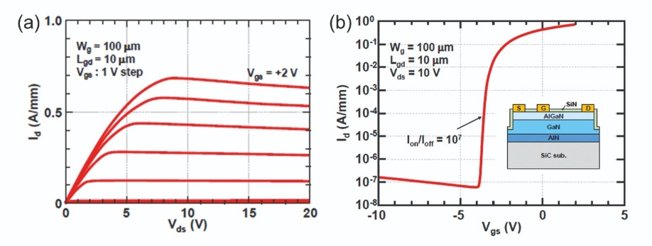
Figure 1. (a) DC plots of the drain current as a function of drain-source voltage (a) and gate-source voltage (b) for a power HEMT produced with SweGaN’s buffer-free GaN-on-SiC technology.
The success of our material hinges on its capability to withstand a high electrical breakdown field. According to theory, the critical breakdown field of GaN is approximately 3 MV/cm. We are not far from that upper limit, with a recent study based on a two-terminal lateral breakdown test showing our material can handle close to 2 MV/cm. That figure, obtained on a structure featuring a 200 nm-thick GaN channel layer, a 60 nm AlN nucleation layer and no field plates, is far higher than that for GaN-on-silicon devices with a carbon-doped buffer – for that class of HEMT, even with the benefit of field plates, the breakdown electrical field is typically 0.6-0.7 MV/cm.
Device testing
To further explore the potential of our buffer-free technology for power applications, we have collaborated with the research group at the University of Fukui, Japan, led by Masaaki Kuzuhara and Joel Asubar. This team, which has been developing techniques to increase the breakdown strength of GaN HEMTs for many years, have previously used low-dislocation-density, iron-doped GaN substrates to propel the breakdown field to 1 MV/cm. These devices reach a breakdown voltage of 5 kV.
Our collaborative effort has involved undertaking breakdown tests on buffer-free HEMTs that have a nominal 25 nm Al0.25Ga0.75N barrier and a 250 nm GaN channel layer. These transistors, fabricated using standard technology developed by the University of Fukui, have a 3 µm gate length, a gate-to-source spacing of 3 µm, a 200 nm mesa isolation depth and a SiN passivation layer 150 nm-thick (see the inset of Fig. 1(b) for details of the device configuration).
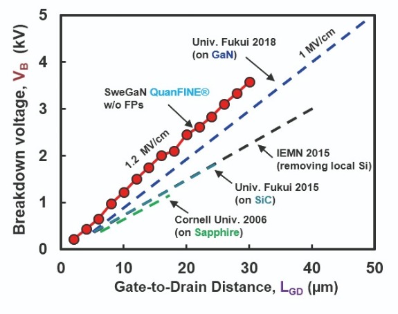
Figure 2. Benchmarking the breakdown voltage at different gate-to-drain distances for GaN HEMT power devices based on different epitaxial growths. Some data comes from J, Asubar et al. “Pushing the GaN HEMT Towards Its Theoretical Limit,” Compound Semiconductor, October 2016, pp. 26-31. In addition, there are results associated with a buffer-free epiwafer measured in this work.
Breakdown tests on a range of our devices, with gate-to-drain distances varying from 0.2 µm to 30 µm, have enabled benchmarking of the critical field strength with state-of-the-art values for GaN grown on different substrates (see Figure 2). As one would expect, the breakdown voltage of our HEMTs increases in a linear manner with the gate-to-drain distance, reaching 3.6 kV at a distance of 30 µm. This translates to a field strength of 1.2 MV/cm, a value higher than that for GaN HEMTs grown on native substrates. Such an impressive result validates the high structural quality of our buffer-free epiwafers, and the effectiveness of using an AlN nucleation layer and a semi-insulating SiC substrate to block high voltages.
Eagle-eyed readers will have spotted that the breakdown field strength for our HEMTs is lower than that recorded for the two-terminal measurement. This discrepancy might result from differences in the methods used to create device isolation. For the two-terminal measurement, a nitrogen ion-implantation provided isolation; and for the HEMTs this resulted from the mesa. We are planning an additional investigation, targeting further optimisation of our buffer-free HEMTs, so that they offer a better breakdown performance.
To put our value for field strength in perspective, the figure of 1.2 MV/cm is four times that for equivalent, commercial, field-plate-free GaN-on-silicon HEMTs (see Table 1). These results show that our buffer-free technology has the potential to reach a lateral breakdown voltage of about 5 kV with standard GaN power device designs.
Table. 1. A comparison of the critical electric field strength, Ec, and the breakdown voltage (VB) for commercial GaN-on-silicon epiwafers and those made by SweGaN, featuring buffer-free technology. Measurements are reported for devices with and without field plates. Note that field plates are commonly used in GaN HEMTs to enhance breakdown voltage. In most cases field plates enhance the magnitude of the electric field strength and the breakdown voltage more than two-fold.
Building on these benchmark results, and in preparation to enter the GaN power market, we have expanded our portfolio of products from 75 mm and 100 mm epiwafers to include those with a 150 mm diameter. Progress with the latter has led to a highly uniform growth process, and deliveries of this new product to customers in the first quarter of this year.
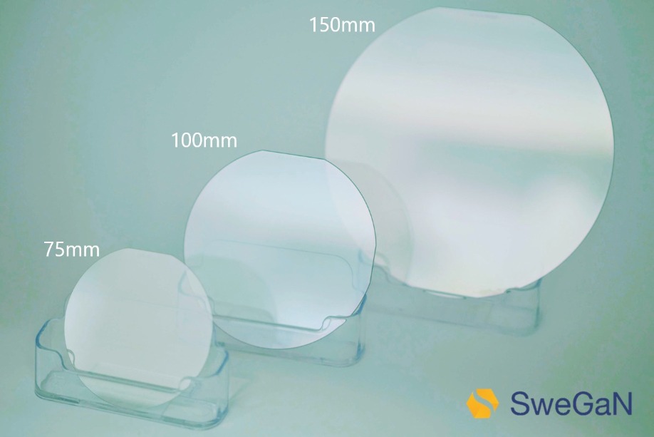
Figure 3. SweGaN’s product portfolio of buffer-free GaN-on-SiC epiwafers.
We are targeting the markets where device performance and reliability are the top priorities for customers and end users. As volumes increases for wide bandgap power electronics, material costs will naturally fall through economies of scale, creating a vast opportunity for our buffer-free technology in the cost-sensitive power market.
Our technology is also destined to enjoy success in the RF device industry. It has already attracted the attention of the majority of GaN RF foundries worldwide, and we expect that it will not be long before it is used in RF device production.
The ECSEL Joint Undertaking (JU) under grant agreement No 826392, UltimateGaN.
J.-T. Chen et al. Appl. Phys. Lett. 113 041605 (2018)
J. Lu et al Appl. Phys. Lett. 115 221601 (2019)
J, Asubar et al. “Pushing the GaN HEMT Towards its Theoretical Limit,” Compound Semiconductor, October 2016, pp. 26-31.
Epitaxial growth on wafer-bonded InP templates enables the integration of high-performance lasers and
Mach-Zehnder modulators with silicon waveguides.
BY Tatsurou Hiraki, Takuma Aihara, Takuro Fujii, Koji Takeda, Takaaki Kakitsuka, Tai Tsuchizawa and Shinji Matsuo FROM NTT CorporatioN
The outbreak of Covid-19 has lead to more teleworking, more steaming of films and more on-line gaming. All of this is driving up global Internet traffic, which had already been growing at an exponential rate for many years. To address this demand, more data centres are being deployed. This solves one problem, but adds to another – humanity’s carbon footprint. To prevent the carbon emissions from this sector escalating to a level where it accounts for a significant fraction of the world’s energy consumption, data centres need to be built with components that draw very little power. To win sales, these products must also be competitively priced and compact, so that they can help to minimise the size of this infrastructure.
A key component in every data centre is the optical transceiver. To increase transmission capacity, it must incorporate Mach-Zehnder modulators, as they enable high baud rates and signals for advanced modulation formats.
One promising technology for meeting these requirements is silicon photonics. It slashes the cost and size of photonic integrated circuits (PICs) by providing ultra-compact waveguide circuits on large, inexpensive silicon wafers. And it has yet another merit: it is compatible with CMOS fabrication technology, an attribute that opens the door to monolithic integration of silicon-based Mach-Zehnder modulators, compact waveguide filters, spot-size converters for fibre coupling, polarization rotators and splitters, and germanium photodetectors on silicon-on-insulator wafers. Today, several companies are drawing on silicon photonics for the design and commercialisation of optical transceivers.
Figure 1. Procedure for integrating III-V semiconductor devices with different bandgaps by direct bonding and epitaxial growth.
There is also another issue with the silicon-based Mach-Zehnder modulator. It has a poor modulation efficiency, because silicon is only able to exploit the inefficient carrier-plasma effect. For this class of modulator, a key figure of merit, known as the half-wave-voltage-length product (VπL), is typically larger than 1 V cm. This high value hampers efforts to trim the size and the power consumption of silicon-based optical transceivers.
An attractive solution to these issues is to heterogeneously integrate III-V semiconductors on a silicon platform. A good choice for this is the InP-based family of materials, which is an established, mature technology for making lasers for telecommunication applications. Another attribute of InP-based materials is that they have a much larger refractive-index change than silicon, thanks to their strong carrier-plasma, band-filling, and Franz-Keldysh effects. These phenomena assist the fabrication of high-efficiency phase shifters for Mach-Zehnder modulators with a small VπL.
Figure 2. Measured photoluminescence intensity distributions of InP-based layers bonded onto SiO2/silicon substrates and annealed at 610 °C for 30 minutes.
A hybrid solution
At the NTT Device Technology Labs in Kanagawa, Japan, our team is developing a novel fabrication method that addresses these issues. Our technology combines direct bonding and epitaxial growth to integrate various III-V devices with different bandgaps on silicon waveguide circuits (see Figure 1).
Fabrication begins by bonding a III-V template to a SOI wafer, and then re-growing different materials on the lattice-matched template, which could be a thin film of InP on SiO2/silicon. Our next step is to use lithographic processes to align and pattern all the III-V devices on the silicon waveguide circuits. With this approach, as well as using epitaxial growth on the lattice-matched template, we can integrate a variety of high-quality materials with different bandgaps. It is this high degree of flexibility that allows us to integrate many high-performance III-V devices.
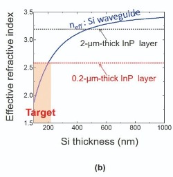
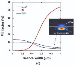
Figure 3. (a) Cross-sectional, scanning-electron microscopy of a membrane laser diode. (b) Calculated effective refractive index of silicon waveguides and InP layers. (c) Calculated fill factors in the multi-quantum well, p-type InP, and silicon cores. The area of the multi-quantum well core is set to 0.6 x 0.1 µm2.
Membrane devices
Our solution is to trim the thickness of the III-V layers, as this reduce thermal strain during the epitaxial growth process. The success of this approach is illustrated in measurements of photoluminescence intensity (see Figure 2). They reveal that there is very little strain in the InP-based layers that are bonded to SiO2/silicon substrates, prior to annealing for 30 minutes in an MOCVD chamber, using the following conditions: 610°C, a PH3 atmosphere and a pressure of 30 Torr. While photoluminescence measurements on structures with 500 nm-thick InP-based layers that include 150 nm-thick multi-quantum-well layers have dark lines, due to exceeding the critical thickness, those that are 250 nm-thick and feature an identical active region are free from degradation, due to the lower thermal strain. These results highlight the necessity of using a membrane structure for epitaxial growth on the silicon substrate.
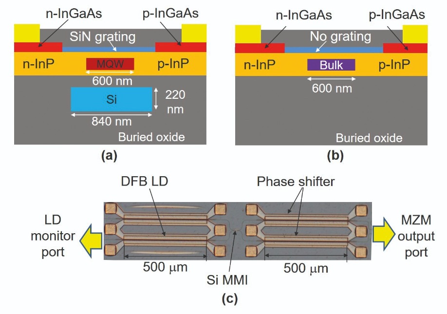
Figure 4. Cross sections of (a) laser diode and (b) phase shifter. (c) Microscopy image of a fabricated laser diode and Mach-Zehnder modulator device.
Using this method, we have fabricated a lateral-current-injection p-i-n diode for the laser diode (see Figure 3(a)). At its heart is a multi-quantum-well core, buried in the 230 nm-thick InP layer and precisely aligned to the silicon waveguide core. This membrane buried heterostructure overcomes another issue facing typical InP-based vertical diodes on a silicon platform – it provides effective refractive-index matching between the III-V and silicon layers.
For optical coupling between the InP and silicon layer, calculations indicate that a typical vertical diode requires a silicon-waveguide layer with a thickness between 400 nm and 500 nm. However, the silicon waveguides widely developed for low-loss and compact channel-waveguide circuits have a thickness of only 220 nm (see Figure 3(b)). In other words, a typical vertical InP-based device is not compatible with these thin silicon waveguide circuits. Fortunately, that’s not the case for our membrane InP-based layer, which is much thinner than the conventional 2 µm-thick InP layer, and comparable to that of the widely used 220 nm-thick silicon waveguide layers. This means that thanks to effective index matching, it is easy to couple our InP-based membrane devices to mature silicon waveguide circuits.
Efficient optical coupling between the multi-quantum well core and low-loss silicon waveguide holds the key to reducing the internal optical loss of the laser diode. Calculations of fill factors in the multi-quantum well core, p-type InP, and silicon cores indicate that thanks to index matching, we can control the fill factors by changing the width of the silicon core (see Figure 3(c)). As a result, overlap with the large-loss, p-type InP region can be reduced by increasing the overlap with the low-loss 220 nm-thick silicon core. Making good use of this, we set the silicon core width to 840 nm to provide a fill factor of around 4 percent in the multi-quantum well. We can change the fill factors of our membrane structure while maintaining the small multi-quantum-well area, enabling us to reduce the threshold current. The upshot of all of this flexibility is that by using the membrane structure, we can obtain high-performance laser diodes on widely developed, 220 nm-thick silicon waveguide circuits.
Integrating laser diodes and modulators
Drawing on the insights provided by our calculations, we have integrated a membrane laser diode with an InP-based Mach-Zehnder modulator on a silicon platform (cross-sections of our membrane laser diode and phase shifter for the Mach-Zehnder modulator are shown in Figures 4(a) and 4(b), respectively). For this particular design, we use a 500 µm-long distributed-feedback laser with a SiN grating on the top of the InP layer. To ensure operation in the C-band, we set the photoluminescence peak wavelengths for the multi-quantum-well core of the laser diode to 1.52 µm, and that for the n-type InGaAsP-bulk core of the phase shifter to 1.3 µm. As both the laser diode and phase shifter are formed in 230 nm-thick InP-based layers, they can be integrated using the epitaxial growth process on a silicon platform.

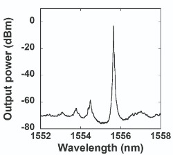

Figure 5. (a) Measured light-output curve from the laser diode port of the laser. The chip facet faced air in this experiment, creating a power fluctuation, due to optical reflection at the facet. (b) Measured output spectrum from the modulator, using a laser diode current of 50 mA and a Mach-Zehnder modulator DC voltage of 4.5 V. A refractive-index-matching oil is inserted between the high-numerical-aperture fibre and the silica core to reduce the reflection at the chip facet. (c) Measured eye diagram for NRZ 28 Gbit/s signal.
Building on this success we have united components, with a 500 µm-long DFB laser diode integrated on the silicon waveguide and connected to the Mach-Zehnder modulator (see the microscopy image, shown in Figure 4(c)). The modulator has silicon multimode interferometers and 500 µm-long membrane phase shifters. At the chip facet there is a silica-based (SiOx) core with an area of 3 x 3 µm2, designed for low-loss fibre coupling. The role of the narrow inverse silicon taper is to convert the optical mode field diameter from the nanowire silicon waveguide to the SiOx waveguide. The SiOx core provides easy butt-coupling to the optical fibre, realising low loss and low reflection.
Our narrow inverse InP tapers are designed to transfer the optical mode fields between the laser diode or phase shifter and the single-mode silicon waveguide. The inverse taper, 50 µm in length and with a cross-sectional area of 0.1 x 0.23 µm2, launches light into the single-mode silicon waveguide that has a cross-sectional area of 0.44 x 0.22 µm2. As the aspect ratio of the taper tip is much lower than that of conventional InP devices, it is relatively easy to fabricate this narrow membrane taper using a mature process. Using this mode converter, we integrate the membrane laser diode and phase shifters with silicon waveguides, realised with low loss and low reflection.
To realise wafer-level integration of both laser diodes and Mach-Zehnder modulators on a silicon platform, we pattern silicon waveguides on a SOI wafer, before burying them in a SiO2 cladding film. Chemical-mechanical polishing of this cladding flattens its surface and reduces its thickness on the silicon waveguide to 100 nm. After this, we remove the InP substrate. The whole multi-quantum well layer is taken away, except for the laser diode region, to leave a 50 nm-thick InP template on the entire wafer. An n-type InGaAsP-bulk layer is then regrown for the phase shifter, before the cores for the laser diode and phase shifter are patterned by lithography. The next steps are: the re-growth of an InP layer to form a buried heterostructure; re-growth of an InGaAs contact layer; and patterning donor and acceptor regions by lithography, followed by their formation with silicon ion implantation and zinc thermal diffusion. The latter step enables us to obtain different carrier profiles for the laser diode and phase shifter on the entire wafer. Completion of the fabrication process involves patterning the InGaAs contact layer and InP mesa and tapers, before turning to a backend process, used to add electrodes and produce a large silica-based core for fibre coupling. By forming the large silica core at a temperature below 200 °C, we avoid damage to the III-V devices.
Proven success
Measurements of output power from the laser diode port, made with a photodetector directly facing a chip facet that detects the total output power coming from it, reveal that the threshold current is only 4.5 mA (see Figure 5(a)). This low value, given the 500 µm active length of the laser diode, is attributed to the small active area. Increasing the injection current to 70 mA propels the output power to around 5.5 mW. This figure indicates that we prevented fatal damage to the active layer during the regrowth processes, and highlights that the membrane InP-based layer is beneficial for reducing thermal strain during the epitaxial growth process.
To evaluate the output power from the Mach-Zehnder modulator’s output port, we aligned a high-numerical-aperture fibre with the silica core at the chip facet. The fibre-coupled output power hits 2.9 mW when driving the laser diode at 70 mA, with tuning of the DC bias of the phase shifter maximising the output power from the measured port. We attribute this high output power to efficient light emission from the membrane laser and to low losses of the Mach-Zehnder modulator and spot-size converter.
Additional measurements reveal that the half-wave voltage (Vp) of the Mach-Zehnder modulator is around 7.5 V. It follows that VpL is around 0.4 V cm, a value more than three times smaller than that of a typical silicon carrier-depletion Mach-Zehnder modulator. These results show that we have succeeded in integrating a high-efficiency InP-based Mach-Zehnder modulator on a silicon platform.
We have also demonstrated dynamic modulation of our laser diode and Mach-Zehnder modulator integrated device. Using a DC bias of 4.5 V for the Mach-Zehnder modulator, to ensure modulation of non-return-to-zero signals, we have investigated the output spectrum at different drive currents for the laser diode. These measurements, made without an RF input to the phase shifter, show single-mode lasing with a side-mode suppression ratio of around 55 dB, for a drive current of 50 mA (see Figure 5(b)).
To evaluate the modulation capability of our design, we have applied RF input signals from a pulse pattern generator to one of the phase shifters in the Mach-Zehnder modulator. This produced a clear eye opening using the following conditions: a laser diode current of 42 mA; a non-return-to-zero 28-Gbit/s signal; without 50 Ω termination at the Mach-Zehnder modulator.
Our next goal is to use our technology to integrate narrow-linewidth laser diodes and in-phase and quadrature modulators for optical transceivers in telecommunication systems. Further ahead, the uses of our platform will expand, as it is not limited to integrating laser diodes and Mach-Zehnder modulators, but can be used to construct other III-V devices with different bandgaps on a silicon platform. This virtue makes our technology ideal for constructing low-cost, large-scale, high-performance PICs with high functionality for various applications.
T. Hiraki et al. “Integrated DFB Laser Diode and High-efficiency Mach-Zehnder Modulator using Membrane III-V Semiconductors on Si Photonics Platform,” 2019 IEEE International Electron Devices Meeting (IEDM), San Francisco, U.S.A, 33.4 (2019)
T. Fujii et al IET Optoelectron. 9 151 (2015)
S. Matsuo et al. Opt. Express 22 12139 (2014)
T. Aihara et al. Opt. Express 27 36438 (2019)

An ultrathin layer of GaN aids electron transport in AlInGaN HEMTs
Engineers at the National Chiao Tung University (NCTU), Taiwan, have enhanced electron transport in InAlGaN-on-silicon HEMTs by adding a GaN interlayer.
This refinement is claimed to strengthen the case for deploying this class of device in 5G communication, in both the handset and the base station.
The team from Taiwan are not the only researchers to have interest in InAlGaN-on-silicon HEMTs piqued by a combination of: a high breakdown voltage; a high cut-off frequency, resulting from the use of thin barrier, enabled by the large polarisation of the quaternary alloy; and a widely available, low-cost, large substrate.
Efforts at NCTU build on previous attempts to improve HEMT performance through the insertion of an AlN spacer layer between an InAlGaN barrier and GaN channel. That earlier work diminished alloy scattering, leading to an increase in electron mobility. Thanks to NCTU, lattice-matching is now improved, by adding a GaN interlayer between the AlN spacer layer and the InAlGaN barrier.
The refined epistructures were grown on a Thomas Swan MOCVD reactor. However, team spokesman Edward Chang believes that with modifications, successful processes could be developed on other MOCVD tools.
Chang reveals that in order to produce a high-quality GaN interlayer, it’s not simply a matter of using the right growth time. It is also critical to optimise the design of the reactor and the flow rate for trimethylgallium, and to carefully select the growth temperature and pressure. “In our experiment, we grow the gallium nitride interlayer with an ultralow flow rate and an ultrashort growth time to prevent decomposition of gallium nitride.”
The team produced a range of samples on 6-inch silicon. All feature a 250 nm-thick AlN nucleation layer, followed by a 600 nm-thick AlGaN transition layer, a 1.1 µm-thick Al0.02Ga0.98N back-barrier, a 500 nm-thick unintentionally doped GaN channel, a 1 nm AlN spacer layer, and a 10 nm-thick In0.11Al0.71Ga0.18N barrier.
A portfolio of devices resulted from inserting GaN interlayers with growth times of 2 s, 4 s, 8 s and 12 s between the AlN spacer and the In0.11Al0.71Ga0.18N barrier. In addition, Chang and his co-workers produced a device without a GaN interlayer.
HEMTs were fabricated by creating mesas with chlorine inductively coupled plasma etching and then using electron-beam evaporation to add Ti/Al/Ni/Nu source and drain contacts and a Ni/Au gate contact, which had dimensions defined by electron-beam lithography. Plasma-enhanced CVD added a 100 nm-thick SiN layer to passivate the HEMTs, which have a 170 nm gate length and a 2 µm source-to-drain spacing.
Atomic force microscopy reveals that there are spiral hillocks in the absence of the interlayer. These hillocks disappear with the introduction of very thin GaN interlayers, which promote a step-flow growth mode. However, as the thickness of the interlayer increases, surface morphology degrades and the step-flow growth mode is almost eliminated.
Chang and his colleagues attribute these changes to decomposition of the GaN interlayer. It degrades until cooled by InAlGaN growth, so the thicker the GaN is, the greater the impact on surface morphology.
Variations in morphology are accompanied by changes in sheet resistance, carrier concentration and mobility – for all these characteristics, the best results are obtained when the GaN interlayer growth time is just 2 seconds. Compared to the device without the interlayer, this HEMT has a far higher current density and transconductance. Using identical operating conditions, values are 1490 mA mm-1, compared with 938 mA mm-1; and 401 mS mm-1, rather than 204 mS mm-1.
The team will continue to develop InAlGaN HEMTs for both high-frequency and power applications. “Also, we will try to develop other nitride materials with even higher polarization,” says Chang.
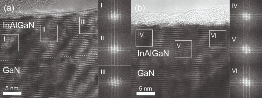
Cross-sectional transmission electron microscopy images of InAlGaN-on-silicon HEMTs without (a) and with (b) a GaN interlayer. Fast-Fourier transform (FFT) images of region I, II, and III identify a tilt in grain orientation, evidence of the poor crystal quality of the InAlGaN layer. FFT images of regions IV, V, and VI are almost similar, implying that inserting a GaN interlayer leads to better crystal quality.
M.-L. Kao et al. Appl. Phys. Express 13 065501 (2020)
Transmission electron microscopy exposes the nature of trench defect formation in InGaN quantum wells
Researchers at Tokyo Institute of Technology are claiming to offer new insight into the formation of trench defects. These defects, found in the quantum wells of long-wavelength light emitters, drag down efficiency.
“Since the trench defect is the most common one found in red-wavelength InGaN quantum wells, where the emission is seriously deteriorated, clarification of this problem helps finding new strategies to realise red InGaN quantum well laser diodes,” says team spokesman Takumi Sannomiya.
By scrutinising samples with transmission electron microscopy, Sannomiya and co-workers discovered that trench defects tend to form where the local indium content is high. These defects have an additional InGaN layer on top of the well that introduces a stacking fault in the GaN capping layer. This allows relaxation of strain resulting from local increases in indium content.
Sannomiya says that two of the promising approaches to efficiently release this strain – a necessity for realising high-performance red GaN laser diodes – are to tune the crystalline orientation and to intentionally introduce another type of defect.
The team from Tokyo Institute of Technology are by no means the first to undertake a detailed study of trench defects in quantum wells. However, previous investigations have failed to draw rigorous conclusions, as they have been unable to rule out the contributions of sapphire substrates and multi-quantum wells to the generation of trench defects.
To overcome these issues, Sannomiya and co-workers have studied single InGaN quantum wells. They are grown on 2-inch GaN substrates from Scios with a threading dislocation density of around 4 x 106 cm-2.
By modifying the growth temperature in the MOCVD reactor, the team produced wells with an indium content of 15 percent, 24 percent, 28 percent, 30 percent and 34 percent, emitting in the blue, green, yellow, orange and red, respectively.
Scanning electron microscopy reveals that V-pits are only found in the samples that emit in the blue and green. V-pit density in the wells of those samples is comparable to the threading dislocation density of the substrates. Trench defects are present in the other samples, with a density increasing from 4 x 105 cm-2 in the yellow emitting well to values of 6 x 107 cm-2 and 7 x 108 cm-2 in the orange and red siblings.
Scrutinising the red-emitting sample revealed that the defect layer in the trench defect is actually in the cap layer, a few atomic layers above the InGaN well.
By studying the positions of the gallium and indium atoms, to determine the local strain, the researchers found evidence for an additional layer of InGaN above the trench. This layer can introduce strain or an interfacial lattice mismatch at the edge of the trench defect. The induced strain may be relaxed by a Basal stacking fault.
Another consequence of the features surrounding the trench defect is an increase in the quantum-confined Stark effect, which leads to a reduction in efficiency. This has been investigated by the team, using cathodoluminescence. Compared to defect-free regions, those with trench defects have an emission that is weaker by a factor of three, and red-shifted by 7 nm due to an increase in the local indium concentration.
The team plans to continue this work, so that they can understand how fluctuations in composition occur, and how this triggers defect formation.
Annular bright-field scanning transmission electron microscopy of a trench defect (top), and a close-up of the boundary of the trench defect (bottom).
T. Tang et al. Appl. Phys. Express 13 062004 (2020)
GaN APDs grown on native substrates combine a very high operating temperature with record responsivity
A US team is claiming to have set a new benchmark for the high-temperature performance of avalanche photodiodes (APDs).
These GaN-on-GaN APDs, made by a collaboration between Stanford University, the University of California, Davis, and San Francisco State University, operate at temperatures of up 250 °C.
“That’s where silicon APDs cannot survive, making this work a unique and important contribution to this field,” argues team spokesman Srabanti Chowdhury, who is currently affiliated to both Stanford University and the University of California, Davis.
By increasing its operating temperature, APDs could serve in new applications in medicine, defence and optical communications.
According to Chowdhury, another strength of these GaN-on-GaN APDs is that they combine a record responsivity with a low dark current.
One concern might be the high cost of the device, given the price of GaN substrates. However, the price of GaN substrates should come down over the next few years.
“Also, keep in mind that the current price of a single silicon-based APD is as high as $100,” says Chowdhury. “This is the case even with silicon’s price being negligible.”
To produce their devices, the engineers begin by depositing a 1 mm-thick, magnesium doped p+ GaN layer on a free-standing substrate. After removing the residual impurities on the surface with UV ozone and HF treatment, they add a 1 mm-thick n-type GaN drift layer and a 200 nm-thick n+ GaN layer.
The next step involves the activation of magnesium ions. To realise this, the researchers etch a 1.4 µm-thick mesa, before using rapid thermal annealing to drive diffusion of hydrogen through the sidewalls.
By employing a two-step magnesium ion implantation process for device-edge termination, rather than just using a solitary step, Chowdhury and co-workers realise a lower leakage in their devices. To complete the fabrication of the APDs, the researchers add a Ni/Au metal stack for the anode and a Ti/Au metal stack for the cathode.
Measurements reveal that the APD’s breakdown voltage is 278 V at room temperature, an increases with temperature in a similar manner to that of variants made from silicon and other compound semiconductors. The dark current at room-temperature, measured at 95 percent of the blocking voltage, is just 1.5 x 10⁻⁵ A cm-2. And thanks to the wide bandgap, this current increases with temperature at a far lower rate than that for commercial APDs made from silicon and InGaAs.
At operating conditions that lead to a controlled avalanche breakdown, the APD produces electroluminescence, with a peak at 410 nm. This emission, claimed to be the first for a GaN APD, results from diffusion of magnesium from the p+ GaN layer into the top layers, to create recombination centres.
When not operating in an avalanche regime, peak photoresponsivity is 0.24 A/W, corresponding to a quantum efficiency of 80 percent. Applying a reverse bias of 280 V, a condition that ensures impact ionisation, yields a peak in the responsivity of 60 A/W.
The gain of the team’s APD is 105 at 300 K, and remains constant up to 525 K. This flat response highlights the high-temperature capability of this device.
Chowdhury hopes that the team’s work will open up many possibilities for GaN APDs. Goals for the team are to reduce the dark current and make the devices work at even higher temperatures.
GaN APDs with an active region that has a radius of 100 µm are fabricated using a double-energy magnesium-ion implantation process to compensate for plasma damage (left). Electroluminescence is observed with a range of avalanche currents.
D. Ji et al. Appl. Phys. Lett. 116 211102 (2020)