EV Sales Growth Depends on Fast Charging, Better Batteries
Replacing fossil-fueled automobiles and light trucks with electric vehicles (EVs) depends heavily on faster charging options paired with robust new battery technology.
EV sales continue to inch upwards. But real growth depends on two essential elements: fast charging stations that mimic the refueling speed of conventional vehicles along with safer, robust battery technology.
Anyone interested in reducing global warming or similar hot-button environmental issues has likely considered an electric vehicle. Choices are now expansive, and thanks to companies such as Tesla Motors, we know EVs can be stylish as well as eco-friendly. But if sticker shock does not deter a purchase, the spectres of range anxiety and achingly long recharge cycles likely do the trick.
Sales of hybrids and all-electric vehicles have accelerated since 2005. But according to Goldman Sachs, EVs will comprise just 3 percent of global light vehicle sales in 2016. EVs clearly lag in popularity with purchasers. While new car manufacturers are steadily enhancing EV options, obstacles remain.
Battery manufacturers know there is the potential for dramatically increasing sales if they can eradicate range anxiety and safety concerns. In response, Tesla Energy has expanding its Giga Factory battery plant with a Panasonic partnership. Tesla has also increased the capacity of PowerWall stationary residential storage while doubling cells in its Powerpack for industrial requirements.
The quest for more and better batteries is also exemplified by Mercedes-Benz Energy that is expanding its Accumotive business in Kamenz, Germany by at least (USD) $500 million. Mercedes is typically coy about its complete end game, but company spokespeople said the expansion will support stationary energy storage products as well as 10 new EV models.
Now that Tesla and one of the world’s most established (and conservative) automobile makers are upping their investments in energy storage and EV batteries, what remains to hold-back the EV market? In two words: fast chargers.
Today’s EV chargers, also called electric vehicle supply equipment (EVSE), tend to come in two flavors: Level 1 (110V) that recharges a vehicle overnight, and Level 2 (240V) that shortens recharging to ‘only’ 8-9.5 hours. While some EVs like the Chevrolet Bolt due out in 2017 are equipped for DC Fast Charge (Level 3), this equipment is rare and typically found only in municipal parking garages or experimental facilities. A Level 3 charger can do its job in less than four hours. Creeping into the market are so-called Level 4 ultra-fast charging stations like the Tesla ‘Supercharger’ that can refuel an EV in one hour or less, but these are proprietary to Tesla.
The market for EVs is growing. However, range anxiety holds back purchases as does the fact that unlike petrol- or diesel-fueled vehicles, refilling an EV’s supply isn’t as fast or easy as it will be one day. Still, encouraging signs abound. Major battery makers like Panasonic and LG Chemical are expanding capacity and improving technology; auto makers like Mercedes-Benz and Tesla Motors are going all-in to develop better batteries and faster charging stations. Once recharging an EV can be accomplished in an hour and battery reliability grows, EVs will take their place in the mainstream. That day cannot come too soon.

ON Semiconductor has agreed to sell its ignition IGBT power device business to Littelfuse for $104 million to allow its acquisition of Fairchild Semiconductor to go ahead.
ON Semiconductor made the approach to Fairchild back in November last year but has had regulatory problems in the $2.4 billion deal.
The merged company would have a combined share of over 60 percent in the worldwide market for Insulated-Gate Bipolar Transistors specifically designed and calibrated for automotive ignition systems, or Ignition IGBTs. Without a
ON Semiconductor has agreed to sell the Ignition IGBT business to Chicago-based manufacturer Littelfuse within 10 days of the close of the transaction. This includes design files and intellectual property that Littelfuse needs to manufacture ON’s Ignition IGBTs. ON must also support the transfer of its customer relationships to Littelfuse, and supply Ignition IGBTs for
The portfolio has annualized sales of approximately $55 million and is expected to close in late
Littelfuse also plans to invest approximately $30 million in its semiconductor fabrication locations to enhance its production capabilities, add significant capacity to its China fabrication facility and transfer the production of the ignition IGBT devices over the next few years, as the company works with customers on their timing and requirements. "Once we complete the transfer of these products, we expect this acquisition to have margins of more than 30 percent," said Meenal Sethna, executive vice
In its 'Power GaN 2016: Epitaxy and Devices, Applications, and Technology Trends' report, Market research firm Yole Développement predicts that the GaN power business will reach $280 million in 2021, growing at 86 percent CAGR between 2015 and 2021.
It says the market is being driven by emerging applications including power supplies for datacentre and telecom, AC fast chargers, Lidar, envelope tracking, and wireless power.
"Numerous powerful developments and key collaborations have been announced during this period and confirmed a promising and fast-growing industry", comments Hong Lin from
Up until late 2014, 600V/650V GaN HEMTs' commercial availability was still questionable, despite announcements from various players. Fast-forward to 2016 (see above) and end users can buy low-voltage GaN (<200V) devices from EPC and high-voltage (600V/650V) components from several players, including Transphorm, GaN Systems, and Panasonic.
The idea of bringing GaN from the power semiconductor market to the much bigger


A master supply agreement between semiconductor firm e2v and GaN Systems has established e2v as the global supplier of GaN Systems' 100V and 650V GaN transistor products and customer care for aerospace and defence (A&D) applications.
e2v will use its infrastructure and 30 years of experience in this area to support the
Mont Taylor, VP of business development at e2v, commented: "Our A&D customers must increase system power density while reducing size and weight. This global partnership with GaN Systems allows us to extend our A&D portfolio and offer new power technologies to meet these requirements."
Larry Spaziani, VP of sales and marketing at GaN Systems, said, "Power designers are routinely reducing the volume and weight of their systems by four to six times by using GaN transistors as a replacement for silicon devices. Partnering with e2v enables our solutions to reach, supply and support hundreds of A&D electronic systems designers. e2v's heritage within the A&D market will allow us to extend the availability of our
With a footprint of 360 x 220 mm the size of a shoebox it is said to be about ten times smaller and has a weight reduction of 80 percent compared to previous generations. The new device has a power density of 1 kW per litre and per kg, an improvement from previous generations by a factor of 15.
The BORDLINE BC battery charger incorporates SiC technology for the first time. “The new battery charger leverages all the benefits available from SiC and soft switching technologies to allow for a new performance level of power electronics in railway," said Sami Atiya, president of ABB's Discrete Automation and Motion division.
"ABB has a long history of providing innovative and energy-efficient technologies to the rail industry and we will continue innovating for the transportation sector, a key growth area in our Next Level strategy."
The new high-speed trains by Stadler operated by the Swiss Federal Railways (SBB) on the new transalpine Gotthard base tunnel route between Zurich and Milan will be equipped with this technology
SiC power semiconductor technology offers significant advantages over traditional silicon-based devices in power applications requiring low losses, high-frequency switching and/or high-temperature environments. For example, the dielectric strength voltage of SiC is about ten times greater than that of Si. Low losses are critical to the performance ratio and SiC technology can reduce the power loss by up to a factor of five. High-frequency switching can be increased from the conventional technology level with a range of 10 to 20kHz by a factor of ten.
Qualcomm Aquisition of NXP Combines Traditional Automotive Force With "New Frontier"
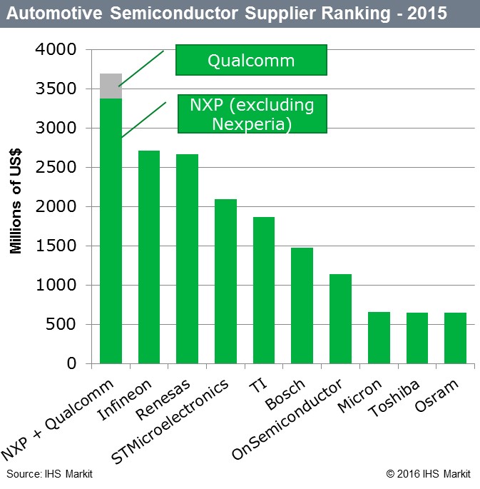
By Ahad Buksh, Analyst and Luca DeAmbroggi, Principal Analyst, Automotive Semiconductors, IHS Markit Technology
The merger Qualcomm and NXP would represent the union of the traditional automotive world with the “new frontier," driven by connectivity and needs for high processing power. NXP’s strength (also through acquisition of FSL) is the reliability and quality standards required in automotive. On the other hand Qualcomm brings its expertise in the connectivity and artificial intelligence applications.
Qualcomm would bring itself to the pinnacle of the automotive semiconductor market in only two years (primarily by buying market shares):

In the aftermath of Hurricane Matthew
earlier this month, NASA released satellite images showing long, dark swaths
along the Atlantic coasts of Florida, Georgia and the Carolinas.
Some 2 million homes and businesses lost power in the storm. A low-tech and decades-old power grid never had a chance. “It’s really a ‘dumb’ system,” said Zhaoyu Wang, an Iowa State University assistant professor of electrical and computer engineering. Wang and other engineers are working to change that. They’re looking for ways to modernize the distribution system that brings power to our homes and offices. They’re out to make a more reliable power grid for all of us. They want to build a smart grid. “The main purpose of grid modernization is to build an efficient and resilient power grid for the future development of our economy,” Wang said.
Developing a tool that will help utility companies recover from natural disasters, supported as part of a three-year, $1.95 million grant from the U.S. Department of Energy’s Grid Modernization Laboratory Consortium. The project is led by Jianhui Wang of Argonne National Laboratory near Chicago. Iowa State’s Wang is working to produce a software tool that will help utilities quickly locate outages and efficiently dispatch crews to make repairs. The software will incorporate information from new grid monitoring devices and actual data from utility companies. Other new technologies – such as micro grids that generate and store power for individual neighborhoods and automatic switches that can find open lines when some lines go down – can also help keep the electricity flowing. “We know our power system is vulnerable to extreme weather,” he said. “In extreme weather events there are maybe hundreds of outages that have to be repaired and we need to send out crews in the optimal way.” Wang said the goal is to reduce the length of extreme-weather outages by half. In the case of a hurricane, he said that means power would be restored in days instead of weeks.
Wang credited several colleagues for
their support and collaboration on the projects – James McCalley, an Anson
Marston Distinguished Professor in Engineering and Jack London Chair in Power
Systems Engineering; Anne Kimber, executive director of Iowa State’s Electric
Power Research Center; Ian Dobson, the Arend J. and Verna V. Sandbulte
Professor in Electrical and Computer Engineering; and Venkataramana Ajjarapu,
the David C. Nicholas Professor of Electrical and Computer Engineering.
The four grid projects will support
the work of eight doctoral students and one postdoctoral researcher. Wang said
all the research has a common goal that can be appreciated by anybody riding
out a storm:
“We’re always trying our best to do
one thing – enhance the power grid. We want to make it more secure, reliable
and resilient. We’re trying to build a power grid that is modern, flexible and
highly efficient.”


Wolfspeed has introduced a 1000V SiC MOSFET for fast charging and industrial power supplies, that is said to cut component count by 30 percent while achieving more than three times increase in power density and a 33 percent increase in output power.
"Supporting the widespread implementation of off-board charging stations, Wolfspeed's technology enables smaller, more efficient charging systems that provide higher power charging at lower overall cost. This market requires high efficiency and wide output voltage range to address the various electric vehicle battery voltages being introduced by automotive suppliers," explained John Palmour, CTO of Wolfspeed.
"Wolfspeed's new 1000V SiC MOSFET offers system designers ultra-fast switching speeds with a fraction of a silicon MOSFET's switching losses. The figure-of-merit delivered by this device is beyond the reach of any competing silicon-based MOSFET," Palmour added.
Designers can reduce component count by moving from silicon-based, three-level topologies to simpler two-level topologies made possible by the 1000 Vds rating of the SiC MOSFET. The increase in output power in a reduced footprint is realised by the low output capacitance - as low as 60pF - which significantly reduces switching losses.
This device enables operations at higher switching frequencies, which shrinks the size of the resonant tank elements and decreases overall losses, thus reducing heatsink requirements. Wolfspeed has determined these proof-points by constructing a 20kW full-bridge resonant LLC converter and comparing it to a market-leading 15kW silicon system.
Wolfspeed offers a 20kW full-bridge resonant LLC converter reference design, listed as part number CRD-20DD09P-2. This fully assembled hardware set allows designers to quickly evaluate the new 1000V SiC MOSFET and demonstrate its faster switching capability, as well as the increased system power density the device enables.
Toshiba Electronics Europe has announced the launch of two new photocouplers, TLP2767 and TLP2367, for high-speed communications at data rates up to 50Mbps.
TLP2767 is the first 50Mbps product in the industry[1] to achieve both a creepage and clearance distance of 8mm and isolation thickness of 0.4mm for reinforced isolation. It is housed in an SO6L package and guarantees isolation voltage of 5000Vrms (min). TLP2367 is housed in a 5pin small SO6 package, guaranteeing creepage and clearance distance of 5mm (min) and isolation voltage of 3750Vrms (min.). Both packages are 2.3mm (max) low height packages and meet international safety standards including UL1577 and EN60747-5-5.
The new photocouplers guarantee a propagation delay time of 20ns (max), pulse width distortion of 8ns (max) and propagation delay skew of 10ns (max). They can be used to reduce the dead time of various interfaces including inverters, which can contribute to improving the power efficiency of systems.
TLP2767 and TLP2367 utilise on the input side Toshiba's original high output infrared LEDs achieving high output power. This reduces the threshold input current by approximately 20 percent, compared with Toshiba’s older TLP117 product. On the output side, a photo detector IC fabricated with a CMOS process reduces the supply current by approximately 50%, compared with Toshiba’s TLP117. Both photocoupler can contribute to lowering the operation voltage of systems with guaranteed supply voltage of 2.7V to 5.5V, at temperatures up to 125 degrees Celsius. Applications include programmable logic controllers (PLC), I/O interface, photovoltaic (PV) inverters and FA inverters.
[1]In the category of photocouplers, as of August 29, 2016. Toshiba survey.
GD Rectifiers Forecast a Bright Future for Distributors in the Power Electronics Industry
Today power electronics plays a critical role in most aspects of our daily lives, from renewable energy, transportation, aviation, automotive, medical, industrial and electronic devices.
On average semiconductors account for 10% of all total power electronic sales and today our homes are proliferated with power electronic devices: TVs, computers, mobile phones, washing machines, fridges, freezers, cookers, hoovers and energy-efficient lighting.
Distribution plays a massive part in the power electronics industry for numerous reasons, we caught up with Paul Bentley, Managing Director of GD Rectifiers to find out what the future has in store for some of the UK’s biggest distributors.
How has power electronics distribution changed in the last 22 years?
The market has grown considerably over the past 22 years with lots of new innovations and technological developments contributing to the rise of local distributors. The size and growth potential of this market makes it a very competitive industry. With the rise of SMEs competing for low-volume business the market has become very crowded. Annual forecasts for the industry change year on year and these are affected by material costs, demand in innovation and technology, consumer trends and products in the pipeline. The power electronics industry is lucrative market when the demand is high, businesses experience peaks and troughs. A shift in trust and responsibility has changed how the distribution model works, distributors are no longer just middlemen for small companies wanting to purchase products they are now an extension to the big manufacturers and generate their own business through their knowledge and expertise.
What has been the biggest challenges over the past 22 years?
The biggest challenge we’ve faced in distribution over the past 22 years has been the selling of grey market goods. Over the year’s numerous countries have sold many commodities that have not been supplied by the original manufacturer to the market. These commodities are sometimes more cost effective because they are not authentic and purpose-built components by the world’s best manufacturers. However, most people that buy grey market goods are hobbyists or first time buyers that shop elsewhere the second time round.
What does the future of distribution look like?
The future is set to be bright for distributors, with the growth of electric propulsion in the automotive sector and the increased demand for renewable energy devices in the industry, distributors should start to feel the market pick back up in 2017.
Most businesses know the benefits of buying components direct from the UK and from official distributors – they know the quality, lead-time and price of the component is not jeopardised.
Most of the world’s leading power electronic manufacturers use franchised distributors to sell their products (and generally smaller business) regionally and this won’t change. The benefits to a customer using a distributor include: a convenient way of shopping, the distributor acts as a one-stop-shop, allowing a fast manufacturing and delivery process providing an efficient supply chain.
SMEs are important drivers of innovation and technology; they play a significant role in supporting large manufacturers to provide a more secure supply chain.
Distributors have a team of highly experienced technical and mechanical engineers that can offer advice and provide a shorter time to market and by acting as a middleman they provide a smooth purchase process by taking care of the ordering, stocking, pricing and delivery.
At GD Rectifiers, we are a global distributor and manufacturer of power electronic devices to industrial markets. We are a stocking distributor, we hold stock on site for the convenience of our customers, and as a manufacturer we also offer: custom designs, design assistance, technical solutions, prototyping, sub assembly work, production, machining and flexible manufacturing facilities.
How will the internet affect the future of distribution?
More and more distributors are looking at ways to improve the customer’s user journey, this includes both online and offline strategies. Online strategies include: sitemaps, eCommerce websites, product offering promotion, social channels, advertising and analysing consumer buying trends. The offline strategies that distributors are adopting include looking at ways to increase retention and acquisition across the market, exploring new promotional tools and widening their product offering. In such a lucrative industry its everyone’s priority to stand out from the crowd, to nurture relationships and remind customers why they should shop with you.

With the adoption of GaN or SiC still some years away for mainstream utilization, power IC vendors need to provide the markets they serve with high voltage switching devices that are still based on established silicon processes and IGBT technology is certainly one that currently holds a lot of promise. Akhil Nair, Technical Marketing Manager for IGBTs, ON Semiconductor explains why.
Insulated gate bipolar transistor (IGBT) devices are vital components in high performance power conversion (HPPC) circuitry. While power MOSFETs are generally used for low/medium voltage implementations, IGBTs (which have voltage ratings in excess of 1kV) are highly optimized for deployment in challenging higher voltage environments. Improving operational efficiencies and reducing losses are now the fundamental concerns for engineers using these devices. The following article tackles this subject in detail.
While wideband gap technologies, such as gallium nitride (GaN) or silicon carbide (SiC) hold a lot of promise for the future, this is still a long way from being a cost-effective strategy for the vast majority of applications - the unit pricing would just be too high at this stage. It is estimated widespread uptake of GaN/SiC technologies probably remains at least 5-8 years away, as technology maturation and greater economies of scale are needed in order to bring price points down to an acceptable level. So, with this option not yet commercially viable, there is a pressing need for some sort of alternative.
Instead of implementing a move to new semiconductor materials, the industry has to find a way to push the performance envelope of existing IGBT technology. The question is…. how is this going to be done?
Application Demands
Advances need to be made so that high voltage IGBT devices can support the elevated frequency levels that are now being demanded, which often extend above the 20 kHz mark as a minimum for many Hi-Performance Power Conversion (HPPC) application. This sort of performance is being expected in a growing number of application areas - among them hybrid/electric vehicles (HEVs), solar infrastructure, uninterrupted power supply (UPS) units and HEV charging stations. Power efficiencies at these higher frequencies has to improve significantly in these applications (heading towards figures of 95 percent in many cases). This implies that switching losses in traditional IGBT technologies needs to come down in order to meet these application demands.
Combating the thermal issues also associated with IGBTs is also of great importance and should not be overlooked. In today’s complex power system designs, space is normally quite constrained. By improving switching performance and consequently system efficiency, the area that needs to be taken up by heatsinking mechanisms can be minimized. This leads to better board space utilization, lower bill of materials costs, while still ensuring the reliability is maintained.
The only way to enhance the performance characteristics of IGBTs, while staying with Si technology, is to explore new approaches in relation to how these IGBTs are designed. There are 2 important criteria that define IGBT operation and impact most acutely on its power efficiency. Firstly, there is the total switching loss (Ets), which is the sum of the turn-on (Eon) and turn-off (Eoff) switching losses. IGBT switching losses can be substantial, especially when the device is running at higher switching frequencies and/or elevated operational temperatures. Secondly, there is the conduction loss to factor in, which relates to the collector-emitter saturation voltage (VCEsat). An unavoidable trade-off exists between the switching loss performance and conduction loss performance. It does not achieve anything, therefore, to simply concentrate on reducing switching losses. Design engineers need to look at the whole thing, rather than a single element in isolation. It is commonplace to refer to the following figure of merit (FoM):
FoM = VCEsat x Ets
This FoM gives engineers a consistent way by which to benchmark the performance of IGBTs and compare the devices offered by different vendors.
IGBT manufacturing challenges
Virtually all IGBTs today are designed as ‘vertical’ devices i.e. the emitter and gate terminals are patterned on one side of the wafer substrate while the collector terminal is on the other side. The FoM of the device is inversely proportional to the thickness of the wafer the device is constructed on i.e. thinner the wafer the higher the FoM of the IGBT. IGBTs today are routinely constructed on wafers <200µm.
Essentially the most
Next Generation IGBT Solutions
Utilizing the company’s proprietary Ultra Field Stop (UFS) trench technology, ON Semiconductor has now introduced a series of 1200V IGBTs with a very high FoM. The standard 1200 V/ 40 A device made with UFS technology has ~40 percent lower ETS and 15 percent lower VCEsat than the best most devices available in the market today. This means that these devices can offer the high degrees of performance now being stipulated, curbing system energy losses and boosting power efficiency levels.
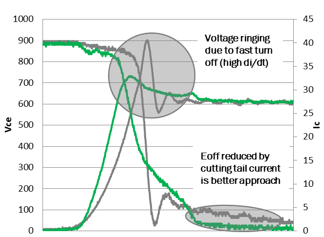
Figure 1
The UFS devices are built on SOI (Silicon On Insulator) substrates. UFS is also the first time that wafers which are only 105µm thick have been used by 1200 V IGBTs. The ultra-thin devices are of course enabled by an extra thick field stop layer. The combination of the thick field stop layer and thin wafers contributes to these devices having such a superior FoM.
Another contributor to the performance improvements delivered by
Figure 3 shows the difference in power losses on a standard half bridge
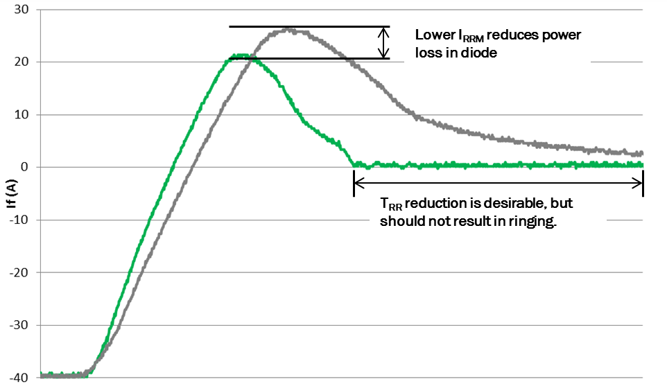
Figure 2
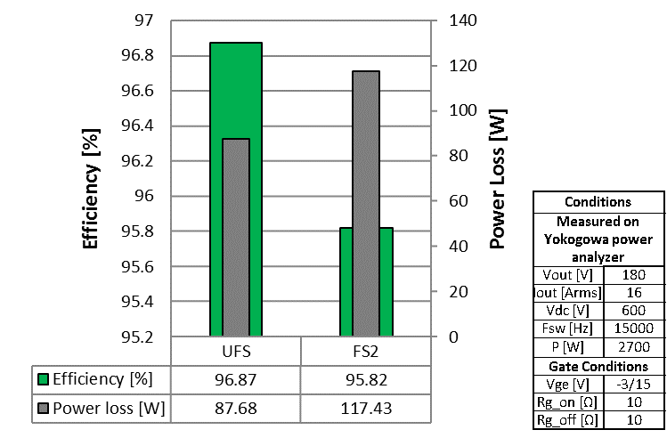
Figure 3
With the adoption of GaN or SiC still many years away, for mainstream utilization at least, power IC vendors need to provide the markets they serve with high voltage switching devices that are still based on established Si processes and IGBT technology is certainly one that currently holds a lot of promise. The combination of newer IGBT technologies such as UFS, combined with advanced fast recovery diode technology has enabled power efficiency levels to be pushed further to satisfy application demands.

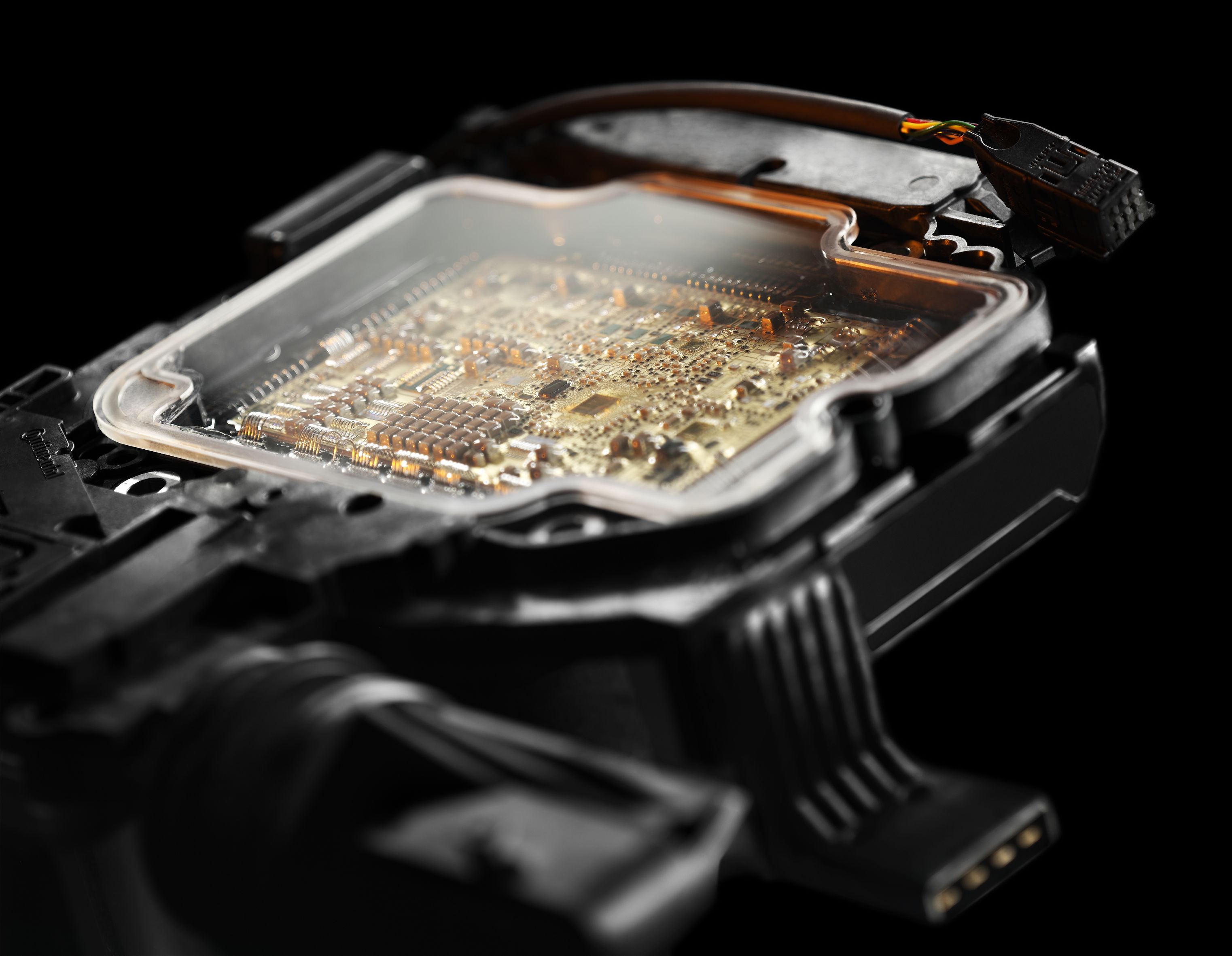
Automotive supplier Continental uses conductive adhesive technology in transmission control modules. Special finishing is required for thermally flexible and high-strength bonding of the components on the modules. For this reason, Isabellenhütte coats
Modern transmissions such as the dual clutch transmission (DCT) increase driving comfort, save fuel, reduce pollutant emission, and are characterized by optimum power delivery. For this reason, Continental is a leader in
Continental uses this process for gluing shunts on the PCB of transmission control modules. The shunts
Conductive adhesive technology establishes the connection between the shunts and the PCB. The adhesive enriched with silver particles is applied to the PCB. It is populated with the shunts. The adhesive is then cured in a furnace and establishes a high-strength connection that is conductive thanks to the silver particles.
The bonded connection is characterized by high reliability and elasticity. Adhesive curing requires approx. 150 degrees Celsius. For comparison: Soldering requires 240 to 280 degrees. Thus,
“To implement this bonding technology in the first place, a high-quality surface is required. For this reason, gold is used for shunt coating,” explains Dipl.-Ing. Anke Schneider from the Continental Business Unit Transmission. Gold coating ensures an improved bonded connection, reliable conductivity, and oil resistance.
The transmission control module is integrated into
The shunts are based on the Isa-Plan technology. Here, a special resistance foil is mounted insulated on a CU substrate. The good heat-conducting substrate ensures a very low thermal internal resistance. The finished shunts can operate at high temperatures under full load without loss of stability or accuracy. Another advantage is a significantly better adopted CET. As a result, the mechanical load of the bonded connection between board and shunt remains very small and ensures a long service life.
The entire contact surface of the PMH-D and PLU shunts are gold-plated. This ensures ideal heat coupling. At 150 degrees Celsius, the shunts are designed for
The VMP shunt is known for its high pulse load capability and very good long-term stability.
At 110 degrees Celsius, it supports a continuous output of 2 Watt and is suitable for continuous currents up to 20 Amps. “A wide temperature spectrum was an important quality criterion for us. A temperature of up to 150 degrees Celsius is reached in the transmission control module. This is our minimum requirement. The VMP-A is even specified up to 170 degrees Celsius,” explains Schneider.

For more driving comfort and reduced consumption:
Continental transmission control module
with conductively bonded, gold-plated Isabellenhütte shunts.
Isabellenhütte’s specialty:
gold-plated shunts.
Mounted on the PCB with silver conductive
adhesive,
they ensure a high-efficient and durable
connection.

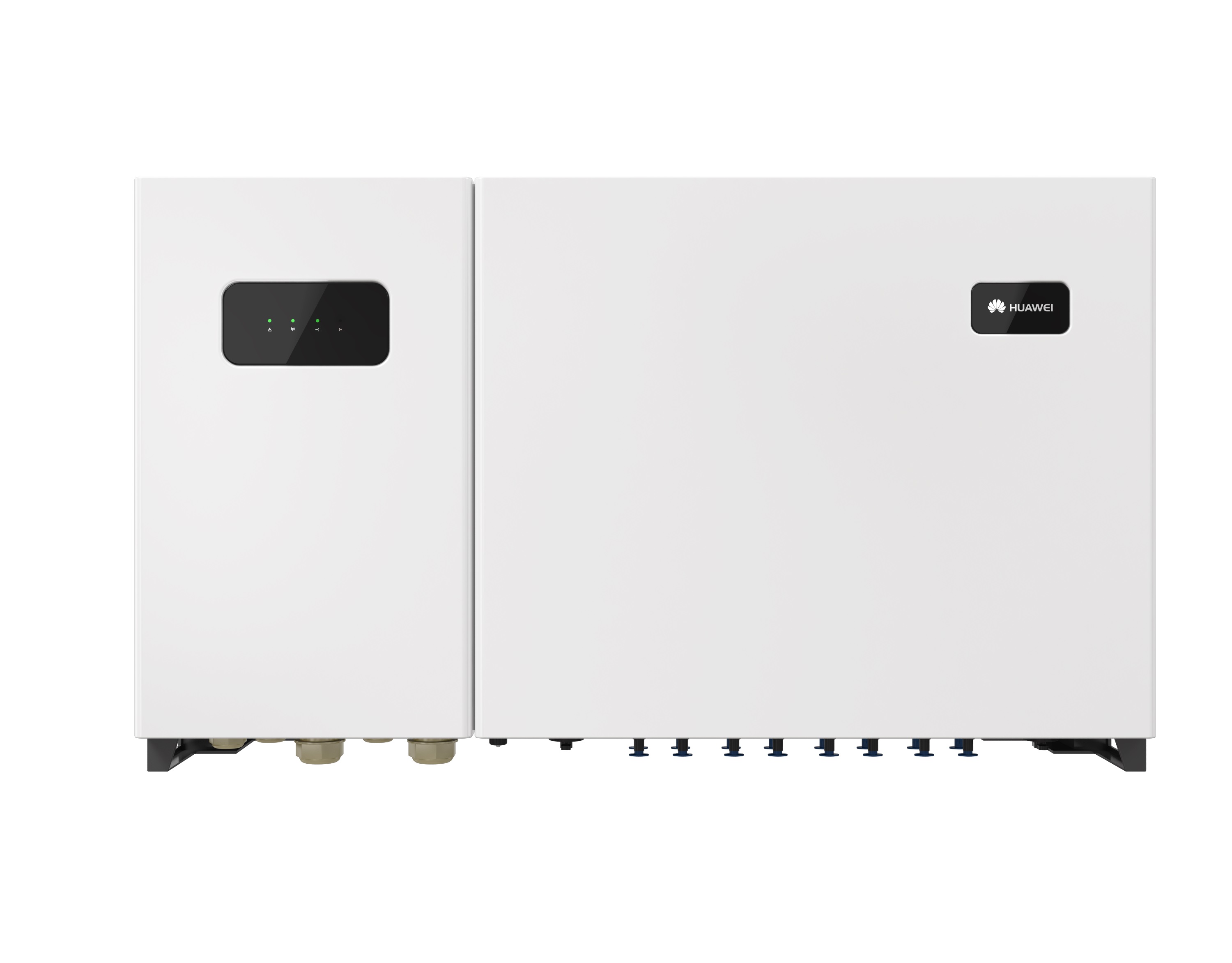
Analysts predict that whilst annual global single-phase and central inverter market revenues will decline, string inverter revenues will grow by 75 percent from 2014 to 2020. Alison Finch, Chief Marketing Officer at Huawei Solar, Europe explains the reasons why.
The utility-scale PV market has had an eventful few years. Installed capacity at the start of 2016 was an impressive 91 GW globally, that’s up from just 5 GW installed at the end of 2010. Solar is now mainstream. It is an established technology in markets such as Europe and North America and deployment worldwide in emerging markets, such as South America, India, and China, continues to grow year-on-year. This success comes in spite of relentless cost pressures and the inevitable rolling back of subsidy support mechanisms in most markets.
The driver of this growth has been an industry-wide focus on innovation and cost-reduction that has seen the
The sum of these small changes is the incredible growth we have witnessed in recent years. But the process continues. We continue to innovate, learn, adapt and ultimately improve. So what are some of the challenges facing utility-scale PV today and how do we overcome them?
In a 2.0MW (AC) array, a Huawei smart PV solution has up to 200 MPPTs. These can optimize power generation by minimizing string mismatch. This is a result of the module cell output fluctuating between +/- 5W per module, then gradually these changes increase by the cells deteriorating with age. However, in a central inverter solution, if one string has a mismatch - like shading - all other strings will be affected. Based on our experience, multiple MPPTs can increase power yields by 1-2 percent. Over the lifetime of a plant, this can add up to a considerable difference in overall yield and return on investment.
Another way to improve yield is through I-V (Current-Voltage) Curve Testing, which EPC’s are contractually required to do annually for 5-10 percent of the site at random. With Huawei’s latest generation of inverters, EPC’s are able to test 100 percent of the site with a click of a button from the convenience of their offices and see the results along with recommendations in less than 15 minutes. This saves time and
The significance of reliability cannot be understated. System failures can be costly and for this reason, EPCs and investors must look to the best–in-class technologies to ensure consistency. The key factors at play with reliability are consistency and containment.
At Huawei, reliability has been a strong focus for our R&D team and the results are bearing dividends. By the end of 2015, Huawei SUN2000 String Inverters accumulated sales of around 15GWs, of which 10GWs (300,000 units) have been connected to the grid for at least one month and the total accumulated failure rate is only 0.35 percent globally and 0.25 percent in the UK.
When things do go wrong, however, the last line of
Related to reliability is the ongoing challenge of the O&M of a plant. If we continue with the previous example of system failure, the other consideration is how quickly repairs can be made so the plant can return to full yield capacity. String inverters are designed to be smaller and therefore easier to install. When one fails, two engineers can replace it with ease in just hours. With the central set-up, in addition to the whole plant being affected by the failure, the repair turnaround is much longer and requires highly skilled engineers, which are certified by the inverter supplier.
A recent IHS survey of customer opinions of string inverters found that the top reason for opting for
Beyond repairs, there are of course costs associated with the daily operation of the two types of inverters. The Huawei SUN2000 Smart PV inverters consume less than 20W power, while in a central inverter solution, power consumption is over 1500W for a 2MW inverter. The Huawei inverter can save 90 percent self-consumption when compared to central, mainly because of our patented natural cooling technology, which does not require a fan.
During the lifecycle of the project, with the central inverter solution, regular fuse replacements are required which incur costs or component
The rapid advance of data and monitoring system has been one of the most exciting developments in our industry. Granularity in real-time monitoring has been an ambition of Huawei since its entry into the solar market. With our background in telecommunications, we felt this was a very natural challenge for us to take on.
When we approach monitoring capabilities our three considerations are
The physical element is just one part of monitoring. Using our Smart Logger, we collect the data and report back from string level monitoring to total the site output. The Smart Logger can also connect to weather stations which
The combination of smart hardware, from the inverter through to the cabling, with intelligent monitoring and reporting, is what Huawei call FusionSolar. The solution lets you monitor and manage multiple PV plants from one control
Companies in the solar industry are often focused on competing with other players in the sector. Yet, the fact remains that we are ultimately in competition with any source of electricity generation that is viable in a target market.
Our competitiveness against other sources of electricity, therefore, remains a vital challenge in securing investment for projects.
We are all responsible as industry players to present a compelling case to investors that outline the benefits of solar. The way to do this is to demonstrate how we are delivering higher yields and greater returns on investment than ever before. Upfront costs and cost pressures generally remain a big issue for the industry. But we must hold a longer perspective and adopt the solutions that deliver over the lifetime of a plant and not give
There is undoubtedly momentum in the market as more and more EPCs and investors opt for string solutions. As the recent IHS Markit report points out, “IHS predicts that whilst annual global single-phase and central inverter market revenues will decline, string inverter revenues will grow by 75 percent from 2014 to 2020.” The evidence of the benefits is mounting and out-dated perceptions are giving way.
As the leading company by shipments of string inverters, Huawei has been at the forefront of this transformation. We are excited about what the future holds, particularly with the integration of smart technologies. We are convinced that the industry is reaching a new milestone when it comes to utility-scale PV through the application of smart technologies. This is a development in which the industry as a whole can find comfort as they continue to invest in this clean energy source.
Alison Finch studied Chemistry at Reading University, then began her corporate career as a graduate trainee for the privately-owned American Corporate, Mars. Over the next decade, her roles there varied from Sales & Marketing to Production Manager in the largest canning factory in Europe, making

Liberté, égalité, batterie: France’s revolutionary role in battery technologies
With
“A new industrial revolution”. That’s how French President François Hollande recently described a form of technology. What would you think he was talking about — robots, automation and industry 4.0, advanced planes or perhaps driverless cars? In fact, Monsieur Hollande was referring to a new lithium battery plant. Batteries are big news in France and they’re constantly evolving. In this piece, Michele Windsor, direct
A French government report from September 2013 details batteries as one of 34 key priorities for French industry. The report discusses the Government's key aspirations — “we want to build a France of long-life batteries” — as well as the key French players innovating the market. These include a number of battery producers, research and development
The global battery market is rapidly expanding and predictions by information and analysis specialist IHS show an increase from $11.8 billion in 2010 to $53.7 billion in 2020. France itself is expected to become the third most valuable market worldwide by 2020. So how does it plan to achieve this?
A key priority is
An example of this is the recent development of sodium-ion batteries by a French team of researchers. These were the world’s first sodium-ion batteries in the 18650 format, as used in torches and laptops. They are small and lightweight, yet have a long life cycle and an energy density which is comparable to lithium-ion.
Sodium is also a more accessible and abundant material than lithium and makes up over 2.6 percent of the Earth’s crust. Although sodium-ion batteries are unlikely to appear on the market for several years, the technology is proof of French innovation in the field.
Despite the extensive R&D taking place in France, it’s clear that lithium-ion batteries are still the most efficient and elegant solution in most applications. Florence Fusalba from the French Alternative Energies and Atomic Energy Commission (CEA) stated that the interest in lithium-ion batteries is because of their universal use.
At Accutronics, we
For example, Iveco Bus is developing ultra-high power lithium-ion batteries to facilitate regenerative braking for use in its hybrid buses. A number of other large French companies, including SNCF, Air France, and France Télécom, have committed to ordering around 50,000 electric vehicles, showing that demand is high in this sector.
The French Government also promotes the country as a nation of start-ups, particularly in fields such as med-tech, where the French medical device market is the second biggest in Europe.
With an
Across Europe, the medical technologies market is growing. With around 7.5 per cent of European GDP being spent on medical technology, the sector is a particular target for professional battery manufacturer Accutronics.
The expansion of the homecare sector in France means that companies increasingly need portable devices which are used to monitor a patient’s condition. It is critical that these devices never fail or run out of battery life at the wrong time, which is why Accutronics has developed its range of smart batteries.
Smart batteries which feature accurate fuel gauging down to a one per cent charge are essential for portable medical devices, which may need to be taken
Smart batteries offer a number of features that are useful in the French medical sector. To prolong the life of the battery, which is particularly useful in the growing homecare sector, smart batteries should have a smart power management system. This means that the battery shuts down when it is not in use, which prevents it from having to be constantly recharged.
This feature is particularly useful when the device is being used once or twice a day, perhaps by a health visitor. Hibernation modes are also effective in saving power. After twelve months of storage, or in high temperatures such as during the summer in the south of France, batteries go into hibernation. This protects internal cells from losing any charge.
To protect the device’s user and the patient, batteries used in the market should feature over protection circuits. These secure the battery against over-temperature, over and under-voltage, overloading and short circuiting. In France, just as in the rest of Europe, regulations are strict for components used in medical devices and it is key that suppliers consider safety concerns and follow these regulations.
President Hollande recently announced that France will boost defence spending by €600 million in 2017. An increase in the defence spend means that the military device market is also key for the French battery industry. This requires a specific knowledge of the requirements for batteries used in the defence industry, such as the necessity for rugged and long lasting batteries.
In early 2016 Ultralife acquired Accutronics, creating a situation where the two companies, specialising in the military and medical sectors respectively, can share their expertise and
Due to recent terrorist activity in France and the surrounding regions, there is also a focus on homeland security. Sensors and other devices required for covert operations have specific battery requirements. The batteries must be long-lasting and must be reliable, meaning that they will not cut out at a key point in their monitoring activity.
Just like in the rest of Europe, counterfeiting is a growing problem in France. In its cornerstone statement on the topic, the French Ministry of Foreign Affairs and International Development says that counterfeit products contribute to destroying 30,000 to 40,000 jobs every year in France and cause a loss of €6 billion for the national economy. This also applies to counterfeit batteries.
With the increase in demand for smart batteries in a number of sectors in France, companies could be tempted to use cheaper batteries which do not come from reliable suppliers. Particularly when containing highly reactive chemicals such as lithium, these could be very dangerous. When smart batteries are used for mission-critical devices, counterfeit batteries have the potential to fail at any time.
However, counterfeit batteries cannot always be easily spotted through a reduced price or different appearance, which is why algorithmic security should be built into the device. As featured in Accutronics’ smart batteries, this technology will either shut a device down when a counterfeit battery is detected or display a warning message. In all applications, this protects the device’s user and the reputation of the device manufacturer. With the prevalence of counterfeiting across Europe, it is important that companies take these measures.
One of our key services at Accutronics is the bespoke design and production of batteries according to our customers' specific needs. Our
The aforementioned French Government report outlines France’s plans towards more renewable energies, “we want to build a France fuelled by renewable energies, less dependent on oil and gas”.
French outlying territories in the Caribbean and off the coast of Africa are currently striving towards reliance on renewable energy. For example, the island of Réunion aims to acquire 100 percent of its energy from renewable sources by 2030. This will require the ability to store large amounts of energy. France is currently developing hydrogen battery storage systems for the remote-site market; the perfect example of how batteries can be designed towards specific needs.
While metropolitan France has a strong reliance on nuclear power, a major pilot project is currently underway, being managed by some of Europe’s largest power network operators, including EDF in France. The Nice Grid project, worth €30m, is working on the viability of using batteries to store renewable energy. It also looks at how citizens can be encouraged to use more of this energy during sunnier periods when more energy is available, rather than in peak evening periods. This project is an example of how new battery technologies could change the way we live our lives and could influence new smart meter technologies.
With
At Accutronics we have similar priorities and our years of experience in the industry, combined with our in-house testing facilities, means we can develop a battery to meet your needs, no matter what the specification. I’m sure if Monsieur Hollande was to come and visit our factory, he’d be considering us part of his new industrial revolution as well. In fact, Monsieur Hollande, if you are reading this, consider it an open invitation!
Dialog's delivery of GaN power ICs signals mainstream market adoption is close
Industry developments including Dialog's recent market entry indicate the GaN power market is gaining more momentum.
Just a few weeks ago, UK-based Dialog Semiconductor revealed plans to sample GaN power ICs in a fast charging power adapter by the end of this financial year.
Following two years of collaboration with Taiwan Semiconductor Manufacturing Corporation, the power management IC supplier has developed a 650V GaN power IC plus controller combination, that is said to
"Until recently, GaN had been largely limited to small specialty fabs from vendors in Japan as well as research institutions," says Mark Tyndall, Senior Vice President of Corporate Development and Strategy at Dialog. "In contrast, Dialog targets high volume consumer applications, so it's never been our intention to prove GaN for, say, niche military applications."
"But when TSMC started to offer GaN as a standard process on six-inch wafers, we saw that as a signal that this was the right time to enter this market as well as solve the emerging problems of size in the power adapter market," he adds.
Dialog's end-result is the so-called SmartGaN DA8801; a monolithic IC that integrates enhanced-mode GaN-on-silicon HEMTs with
By combining this IC with its 'Rapid Charge' power conversion controllers, Dialog can produce efficient, small, high power density adapters that look set to topple traditional silicon FET-based designs from pole position in the world of power adapters
"We're not trying to replace a silicon FET, with a pure GaN transistor; how could a six inch [GaN-on-silicon] wafer process compete with the [CMOS] manufacturer producing millions and millions of wafers?" points out Tyndall. " But we have
"We've reduced the overall bill of materials in our systems and we're getting a lot of excitement as we now have a small 45W adapter in a 25W adapter housing," he adds.
Crucially, this reduction in size paves the way to the universal power adapter that the mobile communications industry craves for its smartphones, notebooks, tablets and more. And according to Tyndall, Dialog customers are more than ready for GaN.
While he reckons initial concerns centered on device reliability, times have changed and industry has moved on. "We're really are beyond these issues now," he asserts.
Indeed, as Richard Eden, senior analyst at IHS Markit, highlights, Dialog is one of many moving towards GaN. "It's a safe bet that all silicon semiconductor suppliers are developing a strategy for GaN," he points out.
"During the last five years, start-ups such as Efficient Power Conversion, Transphorm, and GaN Systems have successfully developed GaN products for the commercial market," he adds. "And more recently, larger silicon semiconductor companies such as Infineon Technologies, Texas Instruments, and Panasonic have announced GaN developments."
For example, in March last year, Texas Instruments launched an 80V GaN FET
For Eden, these developments and Dialog's latest announcement are clear signals that GaN is now joining mainstream markets and is no longer considered to be a 'clever research lab experiment'. "And with foundry companies like TSMC now offering a GaN-on-silicon transistor process technology to clients, perhaps we will see more suppliers offering similar products using their own driver IC [technology]," he says.
Right now, Dialog is testing its GaN-based power IC with Beta customers and is set to sample during Q4, this financial year. The company's next move will be to ramp up production to volume levels, which Tyndall believes will take place by the middle of next year.
"We're strong in the fast-charging, mobile, power adapter market with around a 70% share and we're also entrenched with the top ten vendors in the China smartphone market," he says.
The Development and Strategy President doesn't foresee any supply chain issues - manufacturing uses standard CMOS equipment - but highlights: "We do need to be careful with back-end packaging and have chosen experienced vendors here."
"We also intend to use high volume, standard, device testers which fits with our desire to manufacture hundreds of millions of units without using niche manufacturing processes, equipment or
Then, with wireless device markets addressed, the company intends to turn to PC markets with a 100W power adapter, and eventually target server markets.
Looking beyond high volume consumer markets, Dialog isn't chasing industrial applications such as PV inverters, turbines, and electric vehicles, although according to Tyndall, the company would 'never say never'.
However, the company has settled on GaN-on-silicon as its future technology of choice, over SiC, which Tyndall puts down to lower costs, better monolithic integration, and higher volume production.
"We are looking to drive production volumes now," he concludes. "There is a chicken and egg element here as we need to drive volumes to drive the next level of fab investment that will bring us to a higher wafer size. But I would hope to move to eight-inch wafers in the next two to three years."
High efficiency power conversion is a key requirement whether a utility scale power plant employs photovoltaic (PV) panels or other generation means. Inverter manufacturers offer a wide array of choices to improve performance while reducing CapEx and long-term maintenance costs.
Designing, building and operating utility scale power plants is far from simple. As a bedrock resource of modern existence, electricity affects nearly every aspect of daily life, so it must meet high expectations of consumers, global commerce and multiple regulatory bodies in every country.
Some aspects of power generation and transmission are continually evolving as exemplified by the quest for more efficient PV cells and panels. Other infrastructure elements have been part of ‘the grid’ for so many decades that innovation seems frozen. Yet for power inversion and conversion systems, the times they are a-changing.
Power inverters are lynchpin technology for any plant because they transform generated electricity for transmission and end use. They are also the point at which switching efficiency claims its due; losses reduce available power. Although differences between efficient and less-efficient utility scale inverters/converters may be fractions of a point, the ramifications can be immense across two or three decades of operation.
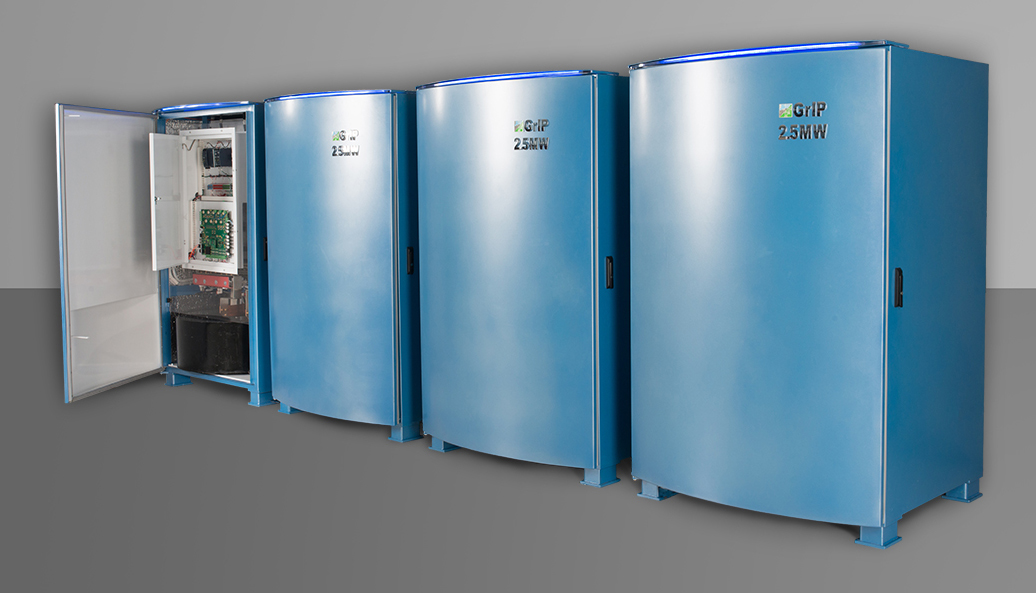
Two very different companies offering products for utility scale photovoltaic (PV) power plants are Alencon LLC and General Electric. While GE traces its roots to Thomas Edison and Nicola Tesla, Alencon is a relative newcomer. The fact that both are building different inverter systems for utility scale PV plants indicates that electricity generation has forever been changed by renewable energy.
General Electric’s latest contribution to inverter technology is its 1500V LV5+ Series with silicon carbide (SiC) transistors delivering 99 percent efficiency. Power Electronics World (contributor) Mark Andrews spoke with Vincent Schellings, GE Power Conversion’s product line leader for power electronics on the day that GE announced its new system during the 2016 Solar Power International (SPI) conference (Las Vegas, Nevada, USA).
“In 2012 when we launched the original system, it was all about Capex (capital expenditures.) Now, this system is about increasing efficiency yield, enabled by silicon carbide. We have been continually investing in this technology, and SiC makes particular sense for renewables because its role in the power stack enables the system to act more efficiently,” he noted.
Schellings explained that the overall efficiencies of their new system yields over $2.2 million (USD) of added value over the lifetime of a 100 MW solar plant, enough to power 170 additional households per year. Another benefit of GE’s system is its new main transformer sleep feature option, which can eliminate no-load transformer losses at night by precisely controlling pre- and de-magnetization of the main transformer. This enables safe connection/reconnection during non-generating hours, saving up to (USD) $800,000 over a plant’s lifetime.
Alencon approaches increasing efficiency through their multi-megawatt central inverter system (MMCIS) that provides installation savings by reducing the quantity and size of DC cables. Savings also come from eliminating all but one inverter installation, and abolishing intermediary AC transmission. Additionally, it provides DC harvesting string inverter conversion granularity and installation simplicity, which increases energy yield. PV panels are connected to string power optimizers and transmitters (SPOTs) that harvest the maximum amount of energy from each string. Additionally, SPOTs convert the strings' low voltage/high current into high voltage/low current DC transmission to minimize losses and reduce cable costs. Combined benefits reduce the levelized cost of electricity (LCOE) by at least 10 percent, according to Alencon President Hanan Fishman, who also indicated his company’s system delivers efficiency as high as 99.5 percent.
In the Alencon system, all optimizers’ outputs are connected to the common DC bus of a single inverter system. The inverter units are modular, so the company says it is easy to add or remove units with minimal effect on the overall system. AC outputs of each module are combined on one or multiple output transformers to raise the AC voltage to that of the electrical grid. The system master controller (SMC) manages operation of the PV plant’s generation system and provides a single interface for the MMCIS. A local monitor collects performance data from every string, SPOT, and grid inverter package (GrIP) in the system, which can be viewed by customers, engineers, and operators through a proprietary real-time graphic display system from anywhere in the world.
While being well-suited for Greenfield construction, Fishman said the majority of their current customers are augmenting and improving older, megawatt-scale PV plants to increase yields and efficiencies while gaining greater performance data. The company’s software and hardware enable relatively quick improvements, which benefit a company’s bottom line once fully implemented.
Increasing yields and improving plant operational efficiency are key objective of both owners and operators. Whether through advances made possible by incorporating silicon carbide (SiC) transistors and ‘sleep mode’ transformer options, or by redesigning the basic inverter concept, the trend towards improving the LCOE of PV power is continuing. Plant owners and operators have new advantages to consider that can improve profitability while demonstrating that electricity generation is changing for the better.

Following €4 million investment, SiC player, Ascatron, aims to deliver very high voltage diodes to market in a year. Chief executive, Christian Vieider, reveals plans.
Ascatron is heading for high voltage markets with its epitaxy expertise [Ascatron].
Just last month, Sweden-based SiC power semiconductor developer, Ascatron, revealed it had raised a hefty €4 million in financing from investors in Italy and China, as well as reactor supplier, LPE, Italy.
Now intending to complete development of its initial SiC devices - the first of which will be a high voltage SiC diode - the company will split funds between materials production and product development.
As Ascatron chief technology officer, Adolf
"We've already started to implement our advanced material technology in production equipment for SiC epitaxy," he adds. "The next step is to
From the late 1990s, researchers at Swedish research institute,
At the same time, development of SiC device concepts, including a normally-off SiC JFET rated to 1.2 kV and 50 A, was well underway. And collaborations with HOYA, Japan, had led to a 3C-SiC process for power MOSFETs.
Fast-forward to today and progress has clearly continued. Ascatron has developed myriad processes for manufacturing SiC semiconductors for power electronics, including substrate buffers, SiC epitaxy, deep trench etching and more.
At the heart of these breakthroughs lies so-called 3DSiC technology, based on embedded epitaxial growth methods that replace the conventional process of doping with ion implantation during SiC device fabrication.
When fabricating SiC devices, doping via ion implantation can bring problems. Ion diffusion is slow, preventing healing of defects, and inhibiting current density and high voltage performance. And in a separate issue, electric fields at Schottky contacts and MOS interfaces also stymy device performance.
To side-step these issues, Ascatron epitaxially grows doped material within etched 3D structures, such as trenches, producing high performance, high voltage SiC devices.
For example, when fabricating a Schottky diode, a p-type grid is first fabricated on the substrate surface, via trench etching.
Epitaxial re-growth and
Crucially electric fields at field-sensitive areas of the device are reduced, high electric fields are shifted into the SiC bulk and ion doping implantation damage simply doesn't exist.
As
"Losses are much lower
So with the process honed and cash in hand, Ascatron is currently working with pilot customers and intends to deliver its first device - a high voltage buried grid SiC Schottky diode for industrial process markets - in a year.
"We're targeting high voltage applications - 10 kV devices - for industrial processing as we see some specific needs that we think we can fulfill," says Vieider. "We've identified that IGBT [modules] are available up to 6.5 kV, but above
But how exactly will Ascatron compete with the likes of Infineon, Cree, ST Microelectronics and Rohm? Vieider reckons his company's technology can provide advantages at the higher voltages that competitors' devices haven't yet reached.
"We already have a customer that is looking for high voltage devices, but just can't find a device," he adds. "Silicon devices can be coupled together in series perhaps, but right now there is really nothing on the market, so this is where we are starting."
And with higher voltage devices in place, the company will then look to broadening applications to lower voltages. Indeed, Ascatron recently bought shares in Italy-based start-up, PileGrowth Technology, to develop MOSFETs based on cubic SiC grown on silicon.
The move could open up markets for 300V to 600 V applications and also allow Ascatron to compete with rival technologies including GaN-on-silicon.
"We had a choice and could have targeted lower voltages from the beginning but there are already competitors in this market," says Vieider. "So once our technology has been adopted at the higher voltages, then we will move to lower voltage applications."
To kick-start its journey to commercial devices, the company recently bought a single-wafer,
According to Vieider, the systems were flexible and produced good material quality, but turnaround times weren't fast enough, so a production upgrade was critical. "We're now ready to scale up our fabrication processes for production," he says. "Our latest reactor has load lock, a good turnaround time and very short cooling times"
"We need to do very thick epitaxy - from 0.1
Past company plans had included the purchase of a multi-wafer reactor system, but Vieider reckons his team will get better material quality with a single wafer system. "In
The company currently buys in substrates from commercial suppliers, and going forward, will keep fundamental epitaxy processes in-house while outsourcing remaining production to a commercial foundry.
"In two years we will have a product on the market and will target more and more applications from higher to lower voltages, addressing broader and broader markets," says Vieider. "Beyond this, our target is to be a supplier of SiC power devices for broad applications.
Engineers from the University of Cambridge have created an ultra-low power transistor that can run for a long time without a power source. This technology could be used in various sensor interfaces and wearable devices, or in more autonomous electronics
A newly-developed form of transistor opens up a range of new electronic applications including wearable or implantable devices by drastically reducing the amount of power used. Devices based on this type of
A new design for transistors which operate on ‘scavenged’ energy from their environment could form the basis for devices which function for months or years without a
A newly-developed form of transistor opens up a range of new electronic applications including wearable or implantable devices by drastically reducing the amount of power used. Devices based on this type of
Using a similar principle to a computer in sleep mode, the new transistor harnesses a tiny ‘leakage’ of electrical current, known as a near-off-state current, for its operations. This leak, like water dripping from a faulty tap, is a characteristic of all transistors, but this is the first time that it has been effectively captured and used functionally. The results, reported in the journal Science, open up new avenues for system design for the Internet of Things, in which most of the things we interact with every day are connected to the Internet.
The transistors can be produced at low temperatures and can be printed on almost any material, from glass and plastic to polyester and paper. They are based on a unique geometry which uses a ‘non-desirable’ characteristic, namely the point of contact between the metal and semiconducting components of a transistor, a so-called ‘Schottky barrier.’
“We’re challenging conventional perception of how a transistor should be,” said Professor Arokia Nathan of Cambridge’s Department of Engineering, the paper’s co-author. “We’ve found that these Schottky barriers, which most engineers try to avoid, actually have the ideal characteristics for the type of
The new design gets around one of the main issues preventing the development of
The design also achieves a very high level of
“If we were to draw energy from a typical AA battery based on this design, it would last for a billion years,” said
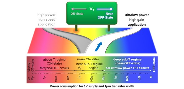
“This will bring about a new design model for
“This is an ingenious transistor concept,” said Professor Gehan Amaratunga, Head of the Electronics,
Reference:
S. Lee and A. Nathan, ‘Subthreshold Schottky-barrier thin film transistors with
Image credit: University of Cambridge
| Publisher/Editor | Jackie Cannon jackie.cannon@angelbc.com +44 (0)1923 690205 |
 |
|---|---|---|
Technical Contributor |
Mark Andrews |
|
| Sales & Marketing Manager | Shehzad Munshi shehzad.munshi@angelbc.com +44 (0)1923 690215 |
|
| Senior Sales Executive | Robin Halder robin.halder@angelbc.com +44 (0)2476 718979 |
|
| Circulation Director | Jan Smoothy jan.smoothy@angelbc.com |
|
| Chief Operating Officer | Stephen Whitehurst stephen.whitehurst@angelbc.com +44 (0)2476 718970 |
USA Representatives
Tom Brun, Brun Media E: tbrun@brunmedia.com +001 724 539-2404
Janice Jenkins E: jjenkins@brunmedia.com +001 724-929-3550
Director of Logistics - Sharon Cowley sharon.cowley@angelbc.com +44 (0)1923 690200
Design & Production Manager - Mitch Gaynor mitch.gaynor@angelbc.com +44 (0)1923 690214
Directors - Bill Dunlop Uprichard - CEO, Stephen Whitehurst - COO, Jan Smoothy - CFO,
Jackie Cannon, Scott Adams, Sharon Cowley, Sukhi Bhadal, Jason Holloway.
Published by
Angel Business Communications Ltd, Hannay House, 39 Clarendon Road,
Watford, Herts WD17 1JA, UK. T: +44 (0)1923 690200 F: +44 (0)1923 690201 E: ask@angelbc.com
Angel Business Communications Ltd, Unit 6, Bow Court, Fletchworth Gate, Burnsall Road,
Coventry CV5 6SP, UK. T: +44 (0)2476 718 970 F: +44 (0)2476 718 971 E: info@angelbc.com
PEW Magazine is published four times a year on a controlled circulation basis. Non-qualifying individuals can subscribe at: £105.00/€158 pa (UK & Europe), £138.00 pa , $198 pa (USA). Cover price £4.50. All information herein is believed to be correct at time of going to press. The publisher does not accept responsibility for any errors and omissions. The views expressed in this publication are not necessarily those of the publisher. Every effort has been made to obtain copyright permission for the material contained in this publication. Angel Business Communications Ltd will be happy to acknowledge any copyright oversights in a subsequent issue of the publication. Angel Business Communications Ltd © Copyright 2016. All rights reserved. Contents may not be reproduced in whole or part without the written consent of the publishers. Power Electronics World - ISSN 2398-9815